


-
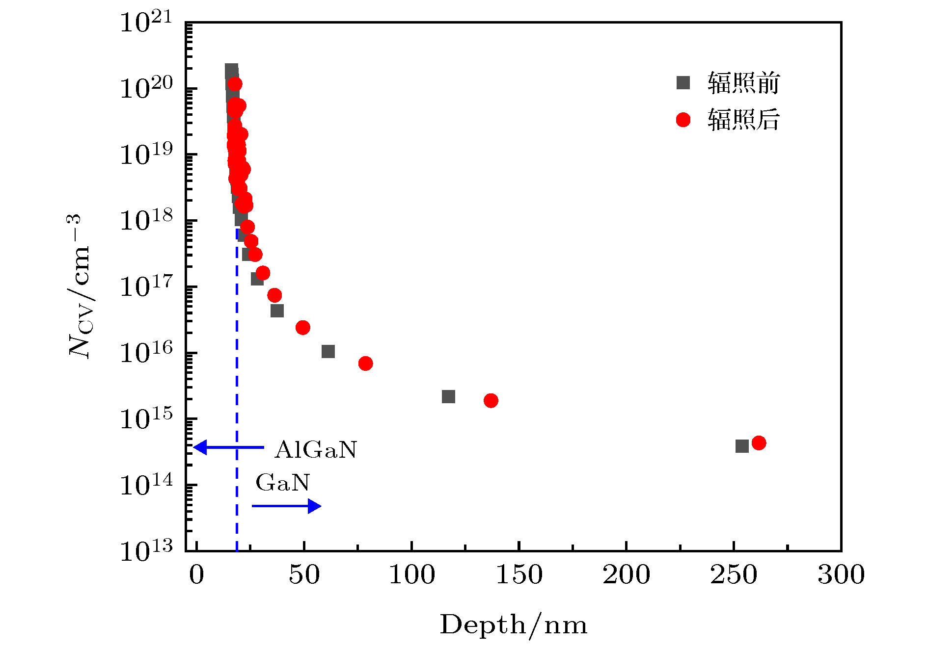
针对AlGaN/GaN高电子迁移率晶体管器件和异质结构在西安脉冲反应堆上开展了中子位移损伤效应研究, 等效1 MeV中子注量为1 × 10¹⁴ n/cm2. 测量了器件在中子辐照前后的直流特性和1/f 噪声特性, 并对测试结果进行理论分析, 结果表明: 中子辐照在器件内引入体缺陷, 沟道处的体缺陷通过俘获电子和散射电子, 造成器件电学性能退化, 主要表现为阈值电压正漂、输出饱和漏电流减小以及栅极泄漏电流增大. 经过低频噪声的测试计算得到, 中子辐照前后, 器件沟道处的缺陷密度由1.78 × 1012 cm–3·eV–1增大到了1.66 × 1014 cm–3·eV–1. 采用C-V测试手段对肖特基异质结进行测试分析, 发现沟道载流子浓度在辐照后有明显降低, 且平带电压也正向漂移. 分析认为中子辐照器件后, 在沟道处产生了大量缺陷, 这些缺陷会影响沟道载流子的浓度和迁移率, 进而影响器件的电学性能.In this paper, neutron-induced displacement damage effects of AlGaN/GaN High electron mobility ransistor (HEMT) device and heterostructure on the Xi’an pulse reactor are studied. The equivalent 1 MeV neutron fluence is 1 × 10¹⁴ n/cm2. The direct-current characteristics and low frequency noise characteristics of the HEMT deviceare used to characterize the performances before and after being irradiated by the neutrons, and then the experimental results are analyzed theoretically. The analysis results showed that the displacement damage effect caused by the neutron irradiation will introduce the bulk defects into the device. The bulk defects at the channel cause the electrical performance of the device to degrade through trapping electrons and scattering electrons, which are mainly manifested as the drift of positive threshold voltage, the decrease of output saturation drain current, and the increase of gate leakage current. In order to further confirm the effect of neutron irradiation on the defect density of the device, we implement the low-frequency noise test and the calculation of the device, and the results show that the defect density at the channel of the device increases from 1.78 × 1012 cm–3·eV–1 to 1.66 × 1014 cm–3·eV–1, which is consistent with the results of the electrical characteristics test, indicating that the new defects introduced by neutron irradiation do degrade the electrical performance of the device. At the same time, the capacitor-voltage test is also carried out to analyze the Schottky heterojunctions before and after neutron irradiation. It is found that the channel carrier concentration is significantly reduced after irradiation, and the flat band voltage also drifts positively. The analysis shows that after irradiating the device with neutrons, a large number of defects will be generated in the channel, and these defects will affect the concentration and mobility of the channel carriers, which in turn will influence the electrical performance of the device. These experimental results can be used for designing the AlGaN/GaN high electron mobility transistor for radiationhard reinforcement.
-
Keywords:
- AlGaN/GaN /
- neutron irradiation /
- displacement damage /
- 1/f noise
[1] 张志荣, 房玉龙, 尹甲运, 郭艳敏, 王波, 王元刚, 李佳, 芦伟立, 高楠, 刘沛, 冯志红 2018 物理学报 67 076801
 Google Scholar
Zhang Z R, Fang Y L, Yin J Y, Guo Y M, Wang B, Wang Y G, Li J, Lu W L, Gao N, Liu P, Feng Z H 2018 Acta Phys. Sin. 67 076801
Google Scholar
[2] Jun B, Subramanian S 2001 IEEE Trans. Electron. Dev. 48 2250
[3] Gu W P, Hao Y, Yang L A 2010 Phys. Status Solidi C 7 1991
Google Scholar
[4] Meneghesso G, Verzellesi G, Danesin F, Rampazzo F, Zanon F, Tazzoli A, Meneghini M, Zanoni E 2008 IEEE Trans. Dev. 8 332
[5] Zhang D X, Chen W, Luo Y H, Liu Y, Guo X Q 2018 Appl. Phys. 9 53
[6] 刘宇安, 庄奕琪, 杜磊, 苏亚慧 2013 物理学报 62 140703
Google Scholar
Liu Y A, Zhuang Y Q, Du L, Su Y H 2013 Acta Phys. Sin. 62 140703
Google Scholar
[7] Jayarman R, Sodini C G 1989 IEEE Trans. Dev. 36 1773
Google Scholar
[8] Fleetwood D M, Shaneyfelt M R, Schwank J R 1994 Appl. Phys Lett. 64 1965
Google Scholar
[9] 彭绍泉, 杜磊, 何亮, 陈伟华, 庄奕琪, 包军林 2008 物理学报 57 5205
Google Scholar
Peng S Q, Du L, He L, Chen W H, Zhuang Y Q, Bao J L 2008 Acta Phys. Sin. 57 5205
Google Scholar
[10] 刘远, 陈海波, 何玉娟 2015 物理学报 64 078501
Google Scholar
Liu Y, Chen H B, He Y J 2015 Acta Phys. Sin. 64 078501
Google Scholar
[11] 董世剑, 郭红霞, 马武英, 吕玲, 潘霄宇, 雷志锋, 岳少忠, 郝蕊静, 琚安安, 钟向丽, 欧阳晓平 2020 物理学报 69 078501
Google Scholar
Dong S J, Guo H X, Ma W Y, Lü L, Pan X Y, Lei Z F, Yue S Z, Hao R J, Ju A A, Zhong X L, Ouyang X P 2020 Acta Phys. Sin. 69 078501
Google Scholar
[12] White B D, Bataiev M, Goss S H and Brillson L J 2003 IEEE Trans.Nucl. Sci. 50 1934
Google Scholar
[13] Rajan S, Xing H, DenBaars S, Jena D 2004 Appl. Phys. Lett. 64 1591
[14] Rashmi A, Kranti S, Haldar, Gupta R S 2002 Solid State Electron. 51 16
[15] Rajan S, Xing H, DenBaars S, Jena D 2004 Appl. Phys Lett. 84 1591
Google Scholar
[16] Delagebeaudeuf D, Linh N T 1982 IEEE Trans. Electron. Dev. 6 955
[17] Xiong H D 2004 Ph. D. Dissertation (Nashville: Vanderbilt University)
[18] Scofield J H, Fleetwood D M 1991 IEEE Trans. Nucl. Sci. 38 1567
Google Scholar
[19] Chen Y Q, Zhang Y C, Liu Y 2018 IEEE Trans. Electron. Dev. 65 1
Google Scholar
[20] 刘宇安 2014 博士学位论文 (西安: 西安电子科技大学)
Liu Y A 2014 Ph. D. Dissertation (Xi’an: Xidian University) (in Chinese)
[21] Casey H C, Fountain G G, Alley R G, Keller B P 1996 Appl. Phys. Lett. 68 1850
Google Scholar
[22] Arulkumaran S, Egawa T, Ishikawa H 2002 Appl. Phys. Lett. 80 2186
Google Scholar
[23] Grove A S 1976 Physics and Technology of Semiconductor Devices (New York: JohnWiley and Sons) pp267−271
-
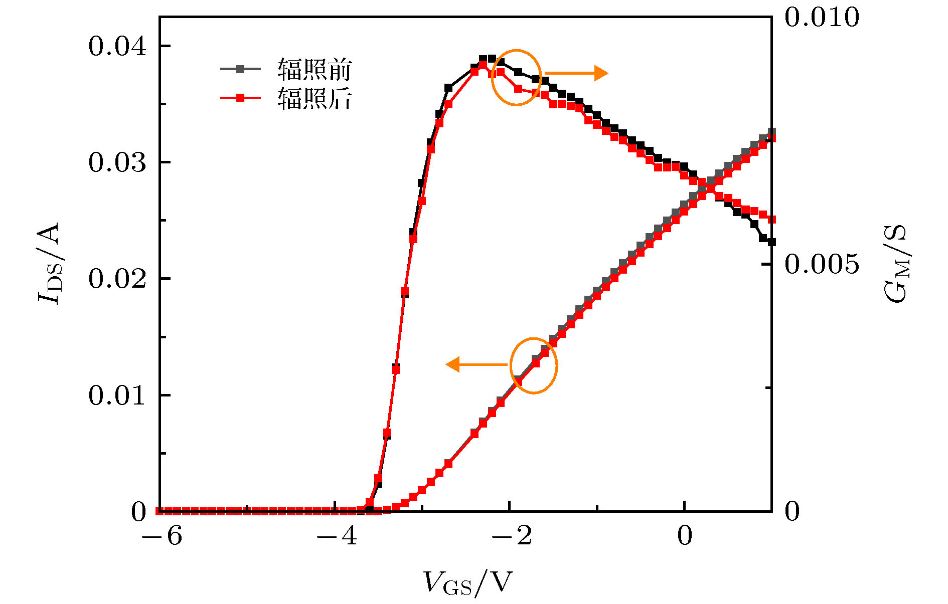
图 2 中子辐照前后AlGaN/GaN HEMT器件转移特性曲线
Fig. 2. Transfer characteristic curve of AlGaN/GaN HEMT device before and after irradiation.
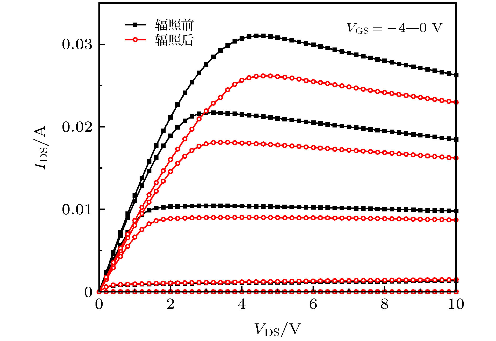
图 3 中子辐照前后AlGaN/GaN HEMT器件输出特性曲线
Fig. 3. Output characteristic curves of AlGaN/GaN HEMT devices before and after irradiation.
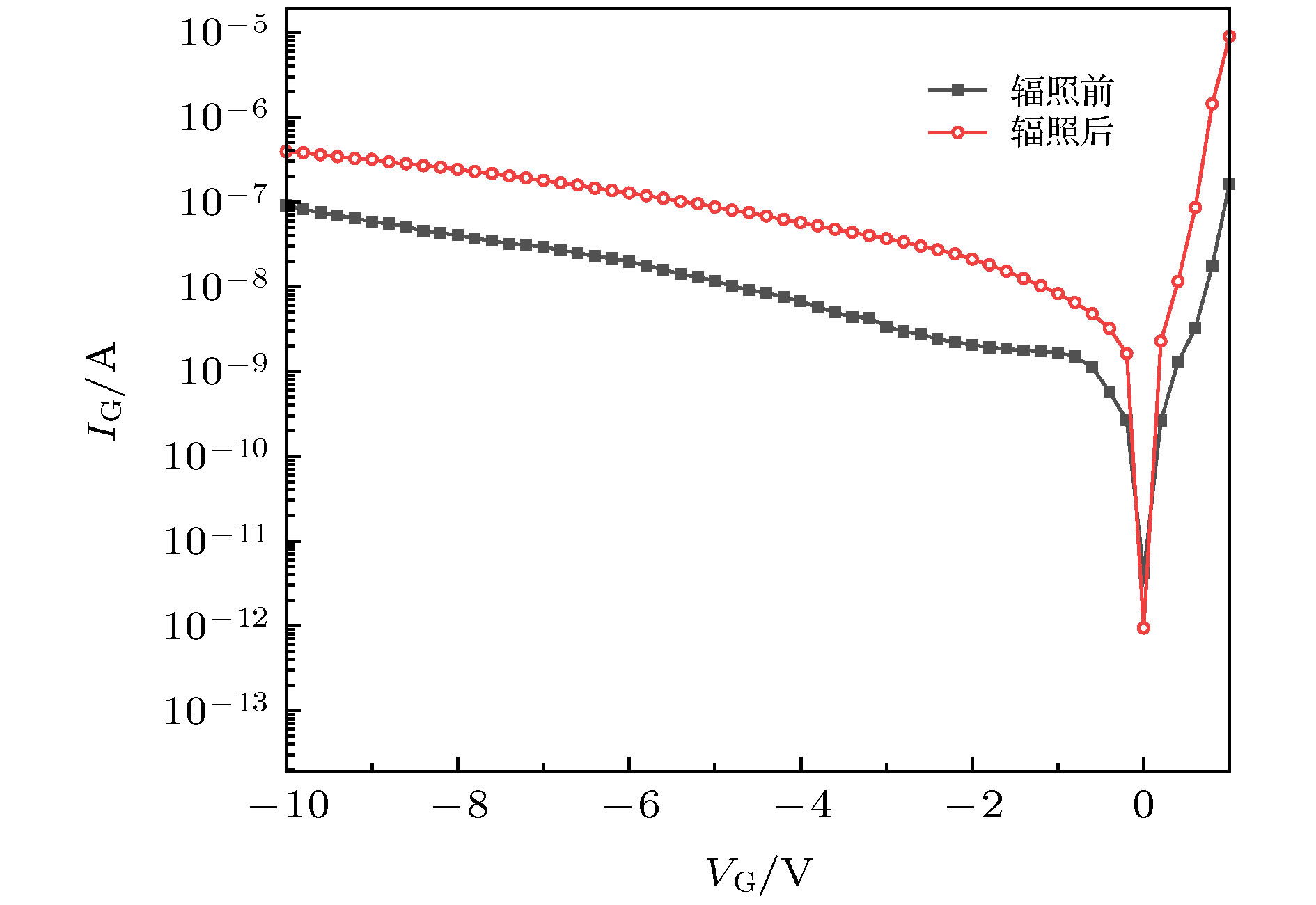
图 4 中子辐照前后AlGaN/GaN HEMT器件栅特性曲线
Fig. 4. Gate characteristic curve of AlGaN/GaN HEMT device before and after irradiation.
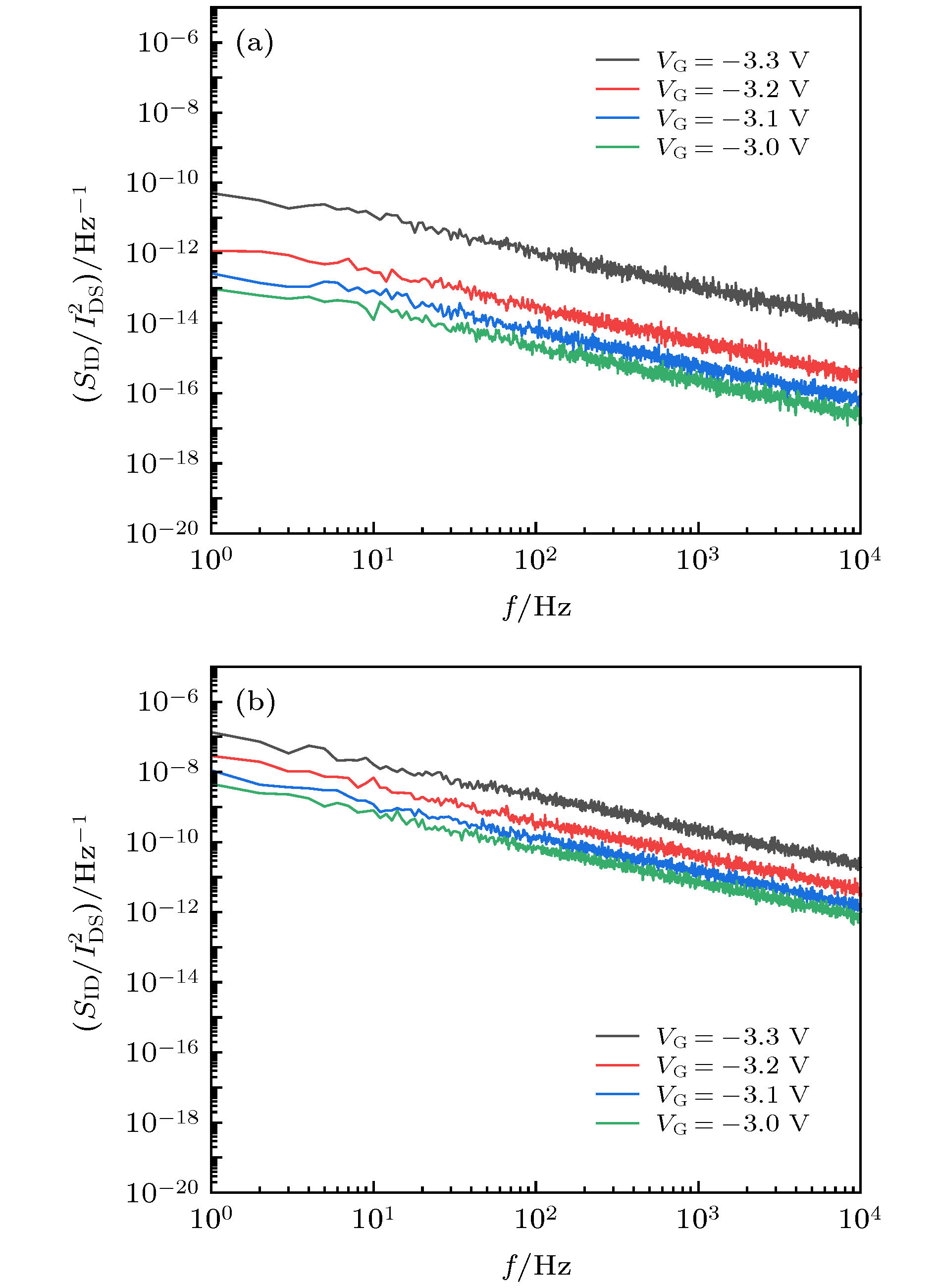
图 5 AlGaN/GaN HEMT器件辐照前与辐照后沟道电流归一化噪声功率谱密度 (a) 辐照前; (b) 辐照后
Fig. 5. Normalized noise power spectral density of channel current in AlGaN/GaN HEMT devices before and after irradiation: (a) Before irradiation; (b) after irradiation.
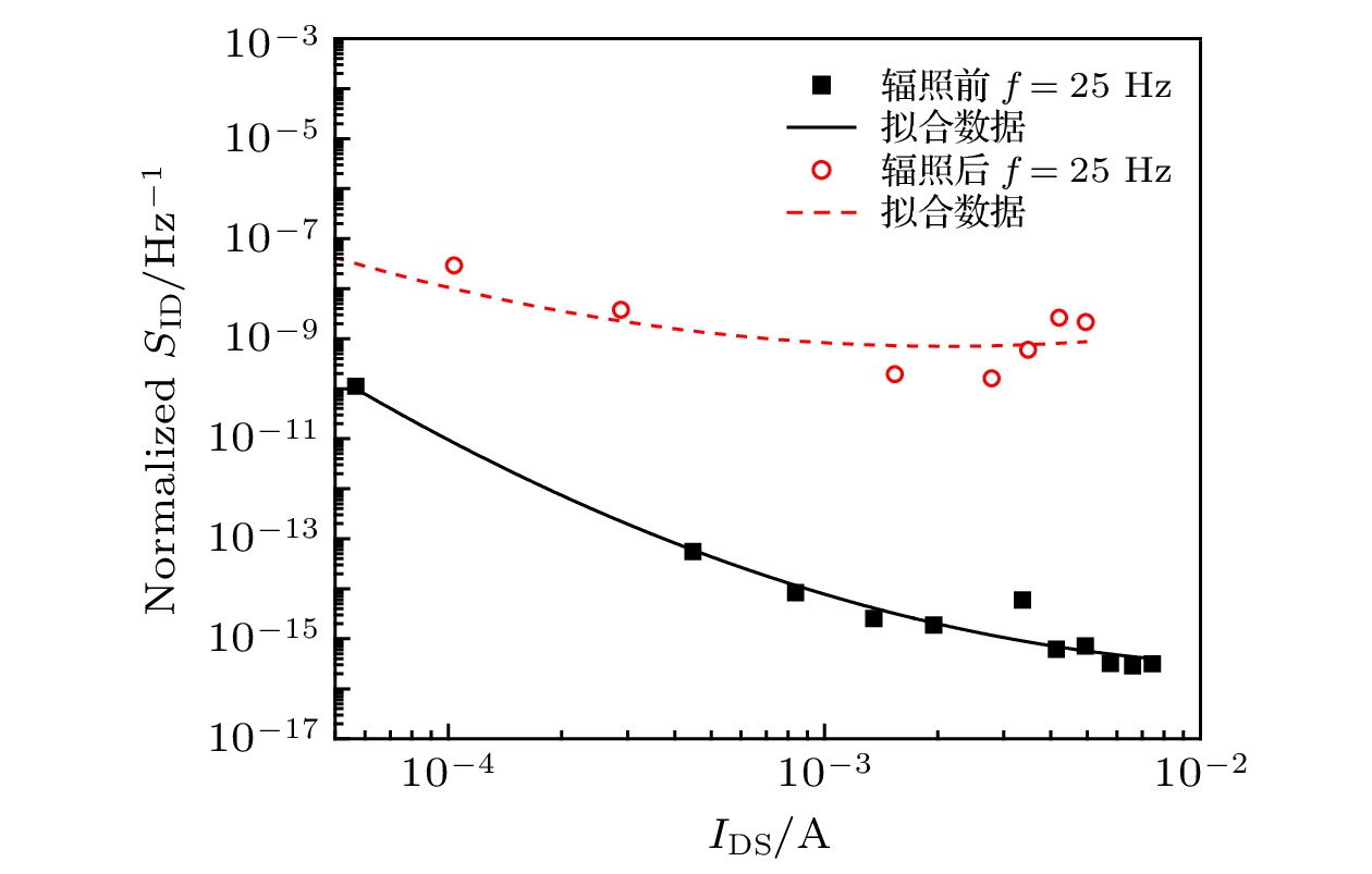
图 6 辐照前后归一化沟道电流噪声功率谱密度与输出电流的关系
Fig. 6. Normalized channel current noise power spectral density versus channel in the AlGaN/GaN HEMT devices before and after irradiation.


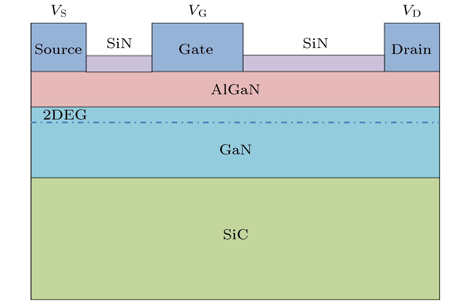
图 8 肖特基二极管器件结构图 (a)剖面图; (b)俯视图
Fig. 8. Schottky diode device structure diagram: (a) Cross-sectional view; (b) top view.
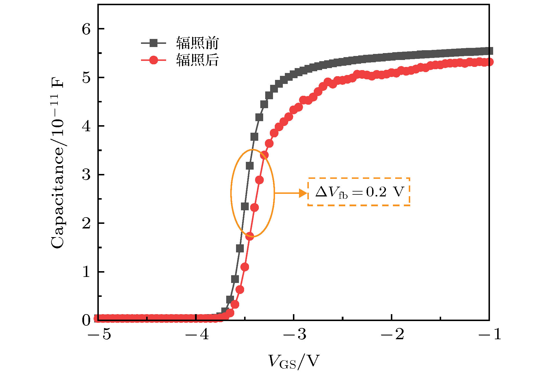
图 9 中子辐照前后的肖特基二极管在1 MHz时电容随偏置电压的变化
Fig. 9. Variation curves of capacitance with bias voltage of Schottky diode before and after neutron irradiation at 1 MHz.
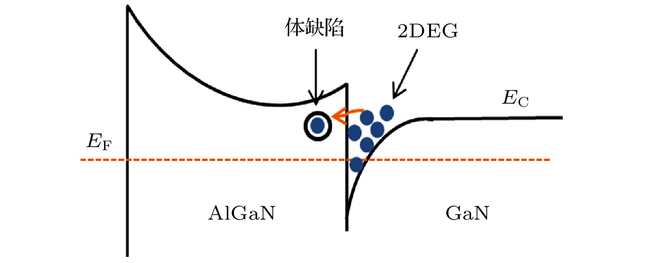
图 11 二维电子气沟道内电子转移到体缺陷示意图
Fig. 11. Schematic diagram of electron transfer to bulk defects in the two-dimensional electron gas channel.
表 1 实验参数
Table 1. Experimental parameters.
直流测试 参数V/V 转移特性 VG = –6—2, VD = 10, VSTEP = 0.1 输出特性 VD = 0—10, VG = –4—1, VSTEP = 1.0 栅特性 VG = –10—2, VD = VS = 0 低频噪
声测试VG = –3.5—–2.0, VSTEP = 0.1,
VD = 10, VS = 0 下载: 导出CSV
表 2 辐照前后噪声参数变化
Table 2. Noise parameter changes before and after irradiation.
参数 辐照前 辐照后 SVfb/V2·Hz–1 1.56 × 10⁻⁹ 1.45 × 10⁻⁷ Nit/cm–3·eV–1 1.78 × 10¹² 1.66 × 10¹⁴
下载: 导出CSV
表 3 实验参数设置
Table 3. Experimental parameters.
直流测试 参数设置: V/V, F/kHz 转移特性 VG = –6—2, VD = 10, VSTEP = 0.1 输出特性 VD = 0—10, VG = –4—1, VSTEP = 1 栅特性 VG = –10—2, VD = VS = 0 C-V 测试 VG = –6—1, VD = 0, VSTEP = 0.05
F=10, 50, 100, 500, 1000, 2000
下载: 导出CSV
-
[1] 张志荣, 房玉龙, 尹甲运, 郭艳敏, 王波, 王元刚, 李佳, 芦伟立, 高楠, 刘沛, 冯志红 2018 物理学报 67 076801
Google Scholar
Zhang Z R, Fang Y L, Yin J Y, Guo Y M, Wang B, Wang Y G, Li J, Lu W L, Gao N, Liu P, Feng Z H 2018 Acta Phys. Sin. 67 076801
Google Scholar
[2] Jun B, Subramanian S 2001 IEEE Trans. Electron. Dev. 48 2250
[3] Gu W P, Hao Y, Yang L A 2010 Phys. Status Solidi C 7 1991
Google Scholar
[4] Meneghesso G, Verzellesi G, Danesin F, Rampazzo F, Zanon F, Tazzoli A, Meneghini M, Zanoni E 2008 IEEE Trans. Dev. 8 332
[5] Zhang D X, Chen W, Luo Y H, Liu Y, Guo X Q 2018 Appl. Phys. 9 53
[6] 刘宇安, 庄奕琪, 杜磊, 苏亚慧 2013 物理学报 62 140703
Google Scholar
Liu Y A, Zhuang Y Q, Du L, Su Y H 2013 Acta Phys. Sin. 62 140703
Google Scholar
[7] Jayarman R, Sodini C G 1989 IEEE Trans. Dev. 36 1773
Google Scholar
[8] Fleetwood D M, Shaneyfelt M R, Schwank J R 1994 Appl. Phys Lett. 64 1965
Google Scholar
[9] 彭绍泉, 杜磊, 何亮, 陈伟华, 庄奕琪, 包军林 2008 物理学报 57 5205
Google Scholar
Peng S Q, Du L, He L, Chen W H, Zhuang Y Q, Bao J L 2008 Acta Phys. Sin. 57 5205
Google Scholar
[10] 刘远, 陈海波, 何玉娟 2015 物理学报 64 078501
Google Scholar
Liu Y, Chen H B, He Y J 2015 Acta Phys. Sin. 64 078501
Google Scholar
[11] 董世剑, 郭红霞, 马武英, 吕玲, 潘霄宇, 雷志锋, 岳少忠, 郝蕊静, 琚安安, 钟向丽, 欧阳晓平 2020 物理学报 69 078501
Google Scholar
Dong S J, Guo H X, Ma W Y, Lü L, Pan X Y, Lei Z F, Yue S Z, Hao R J, Ju A A, Zhong X L, Ouyang X P 2020 Acta Phys. Sin. 69 078501
Google Scholar
[12] White B D, Bataiev M, Goss S H and Brillson L J 2003 IEEE Trans.Nucl. Sci. 50 1934
Google Scholar
[13] Rajan S, Xing H, DenBaars S, Jena D 2004 Appl. Phys. Lett. 64 1591
[14] Rashmi A, Kranti S, Haldar, Gupta R S 2002 Solid State Electron. 51 16
[15] Rajan S, Xing H, DenBaars S, Jena D 2004 Appl. Phys Lett. 84 1591
Google Scholar
[16] Delagebeaudeuf D, Linh N T 1982 IEEE Trans. Electron. Dev. 6 955
[17] Xiong H D 2004 Ph. D. Dissertation (Nashville: Vanderbilt University)
[18] Scofield J H, Fleetwood D M 1991 IEEE Trans. Nucl. Sci. 38 1567
Google Scholar
[19] Chen Y Q, Zhang Y C, Liu Y 2018 IEEE Trans. Electron. Dev. 65 1
Google Scholar
[20] 刘宇安 2014 博士学位论文 (西安: 西安电子科技大学)
Liu Y A 2014 Ph. D. Dissertation (Xi’an: Xidian University) (in Chinese)
[21] Casey H C, Fountain G G, Alley R G, Keller B P 1996 Appl. Phys. Lett. 68 1850
Google Scholar
[22] Arulkumaran S, Egawa T, Ishikawa H 2002 Appl. Phys. Lett. 80 2186
Google Scholar
[23] Grove A S 1976 Physics and Technology of Semiconductor Devices (New York: JohnWiley and Sons) pp267−271

 下载:
下载:
计量
- 文章访问数: 10855
- PDF下载量: 208
- 被引次数: 0
