


-
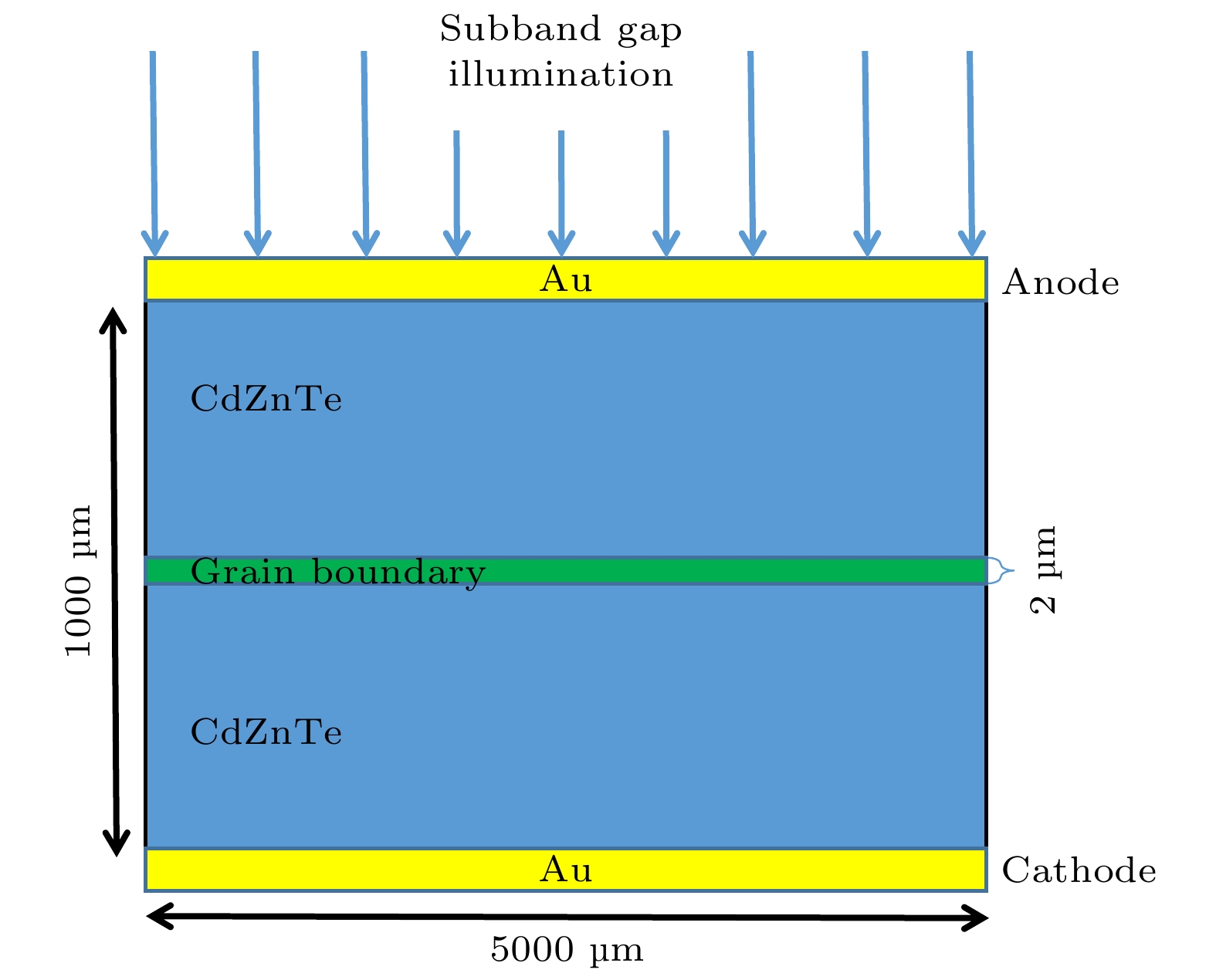
晶界是限制CdZnTe核辐射成像探测器大面积应用的主要缺陷之一. 为了探究改善晶界附近电场分布特性的方式, 本文采用Silvaco TCAD从理论上研究了亚禁带光照对于含晶界CdZnTe探测器内电场分布的影响. 仿真结果表明, 在无偏压下, 亚禁带光照能使得晶界势垒降低, 从而减小对载流子传输的阻碍作用. 在外加偏压下, 亚禁带光照使得晶界引起的电场死区消失, 使其电场分布趋向于线性分布. 同时研究了不同波长和不同强度的亚禁带光照对于晶界电场分布的影响, 结果表明光强低于1×10⁻⁹ W/cm2时, 亚禁带光照对于CdZnTe晶体的电场无调节作用. 而在波长850 nm, 光强1×10⁻⁷ W/cm2的亚禁带光照下, 实现了更平坦地电场分布, 因此可有效地提高器件的载流子收集效率. 仿真结果为调节晶界电场分布提供了理论指导.
Grain boundary is one of the main defects, limiting the large-area application of CdZnTe nuclear radiation imaging detectors. In order to explore the ways to improve the electric field distribution properties near grain boundary, the effect of sub-bandgap illumination on the electric field distribution in CdZnTe detector with grain boundary is studied by Silvaco TCAD simulation technique. The grain boundary potential barrier and electric field dead zone are found in simulation results that significantly affect the carrier transport process in CdZnTe detector. The electric field dead zone caused by the grain boundary disappears under the bias of sub-bandgap illumination. Thus the electric field distribution tends to be linear. Meanwhile, the effects of different wavelengths and intensities of sub-bandgap illumination on the electric field distribution at the grain boundary are also investigated. The results show that the electric field of CdZnTe is distorted by sub-bandgap illumination at an intensity lower than 1×10⁻⁹ W/cm2. In contrast, a flatter electric field distribution is achieved at a wavelength of 850 nm and an intensity of 1×10⁻⁷ W/cm2. The carriers can be transported by drifting, reducing the probability of being captured or recombined by defects during transport, thus improving the charge collection efficiency of the detector. In addition, the microscopic mechanism of the modulation of the electric field distribution by sub-bandgap illumination and the energy band model of CdZnTe crystal containing grain boundary are proposed. Owing to the existence of the grain boundary, two space charge regions are formed near the grain boundary. The energy band at the grain boundary is bent upward. Meanwhile, the metal-semiconductor contact forms a Schottky barrier, and the energy band near the electrode is bent upward. When the bias voltage is applied, the energy band structure of the CdZnTe tends to tilt from the cathode to the anode. The sub-bandgap illumination can lower the energy band barrier at the grain boundary and regulate the energy band on both sides of the grain boundary. It is believed that this discussion will also make some contributions to understanding of the effects of illumination and grain boundary in other types of optoelectronic devices, especially the applications of thin films in solar cells and detectors. -
Keywords:
- CdZnTe /
- grain boundary /
- silvaco /
- sub-bandgap illumination
[1] Johns P M, Nino J C 2019 J. Appl. Phys. 126 40902
 Google Scholar
[2] Kathalingam A, Valanarasu S, Ramesh S, Kim H S, Kim H S 2021 Sol. Energy. 224 923
Google Scholar
[3] 李颖锐, 吴森, 郭玉, 席守智, 符旭, 查钢强, 介万奇 2019 红外与激光工程 48 1016001
Google Scholar
Li Y R, Wu S, Guo Y, Xi S Z, Fu X, Zha G Q, Jie W Q 2019 Infrared Laser Eng. 48 1016001
Google Scholar
[4] Abbene L, Principato F, Gerardi G, Buttacavoli A, Cascio D, Bettelli M, Amade N S, Seller P, Veale M, Fox O, Sawhney K, Zanettini S, Tomarchio E, Zappettini A 2020 J. Synchrotron Radiat. 27 319
Google Scholar
[5] Gao X, Sun H, Yang D, Wangyang P, Zhang C, Zhu X 2020 Vacuum 183 109855
Google Scholar
[6] Chu M, Terterian S, Ting D, Wang C C, Gurgenian H K, Mesropian S 2001 Appl. Phys. Lett. 79 2728
Google Scholar
[7] Carvalho A, Tagantsev A K, Oberg S, Briddon P R, Setter N 2010 Phys. Rev. B 81 075215
Google Scholar
[8] 孙士文, 隋淞印, 何力, 周昌鹤, 虞慧娴, 徐超 2014 红外技术 36 588
Google Scholar
Sun S W, Sui S Y, Li H E, Zhou C H, Yu H X, Xu C 2014 IR. Tech. 36 588
Google Scholar
[9] Parker B H, Stahle C M, Roth D, Babu S, Tueller J 2001 Proc. SPIE. 4507 68
Google Scholar
[10] Zeng D M, Jie W Q, Wang T, Zhou H 2009 J. Cryst. Growth 311 4414
Google Scholar
[11] Markunas J K, Almeida L A, Jacobs R N, Pellegrino J, Qadri S B, Mahadik N, Sanghera J 2010 J. Electron. Mater 39 738
Google Scholar
[12] Bolotnikov A E, Babalola S O, Camarda G S, et al. 2009 IEEE Trans. Nucl. Sci. 56 1775
Google Scholar
[13] Li W, Tkaczyk J E, Andreini K W, Cui J, Zhang T, Williams Y, Harding K G, Chen H, Bindley G, Matyi R J 2009 IEEE Nuclear Science Symposium Conference Record Orlando, USA, October 24–November 1, 2009 p1658
[14] Dong J P, Jie W Q, Yu J Y, Guo R R, Teichert C, Gradwohl K P, Zhang B B, Luo X X, Xi S Z, Xu Y D 2018 Chin. Phys. B. 27 117202
Google Scholar
[15] Prokesch M, Szeles C 2010 US Patent 20100078558 A1
[16] Ivanov V, Dorogov P, Loutchanski A 2011 International Conference on Advancements in Nuclear Instrumentation, Measurement Methods and their Applications Ghent, Belgium, June 6–9, 2011 p1
[17] Washington A L, Teague L C, Duff M C, Burger A, Groza M, Buliga V 2011 J. Appl. Phys 110 073708
Google Scholar
[18] Sik O, Grmela L, Elhadidy H, et al. 2013 J. Instrum. 8 C06005
Google Scholar
[19] Zhang Y Q, Fu L 2018 Mater. Sci. Forum 922 40
Google Scholar
[20] Prokesch M, Szeles C 2007 Phys. Rev. B 75 245204
Google Scholar
[21] Gul R, Roy U N, James R B 2017 J. Appl. Phys. 121 115701
Google Scholar
[22] Zhou Y M, He Y G, Lu A X, Wan Q 2009 Chin. Phys. B 18 3966
Google Scholar
[23] Kong H S, Lee C 1995 J. Appl. Phys. 78 6122
Google Scholar
[24] Kumari K, Avasthi S 2017 IEEE 44th Photovoltaic Specialists Conference Washington, USA, June 25–30, 2017 p251
[25] Hossain F M, Nishii J, Takagi S, Sugiharad T, Ohtomo A, Fukumura T, Koinuma H, Ohno H, Kawasaki M 2004 Phys. E 21 911
Google Scholar
[26] Zhang A, Zhao X R, Duan L B, Liu J M, Zhao J L 2011 Chin. Phys. B 20 057201
Google Scholar
[27] Kim K H, Na Y H, Park Y J, Jung T R, Kim S U, Hong J K 2004 IEEE Trans. Nucl. Sci. 51 3094
Google Scholar
[28] Kim K H, Ahn S Y, An S Y, Hong J K, Yi Y, Kim S U 2007 Curr Appl. Phys. 7 296
Google Scholar
[29] Wei S H, Zhang S B 2002 Phys. Rev. B 66 155211
Google Scholar
[30] Hjelt K, Juvonen M, Tuomi T, Nenonen S, Eissler E E, Bavdaz M 1997 Phys. Status Solidi. 162 747
Google Scholar
[31] Cola A, Farella I 2013 Sensors 13 9414
Google Scholar
[32] Cola A, Farella I, Anni M, Martucci M C 2012 IEEE Trans. Nucl. Sci 59 1569
Google Scholar
[33] Montmorillon L A D, Delaye P, Launay J C, Roosen G 1995 Opt. Mater. 4 233
Google Scholar
[34] Marple D T F 1964 J. Appl. Phys. 35 539
Google Scholar
[35] Schlesinger T E, Toney J E, Yoon H, Lee E Y, Brunett B A, Franks L, James R B 2001 Mater. Sci. Eng. R 32 103
Google Scholar
[36] Hsieh Y K, Card H C 1989 J. Appl. Phys. 65 2409
Google Scholar
[37] Keevers M J, Green M A 1994 J. Appl. Phys. 75 4022
Google Scholar
[38] 徐凌燕 2014 博士学位论文 (西安: 西北工业大学)
Xu L Y 2014 Ph. D. Dissertation (Xian: Northwestern Polytechnical University)
-
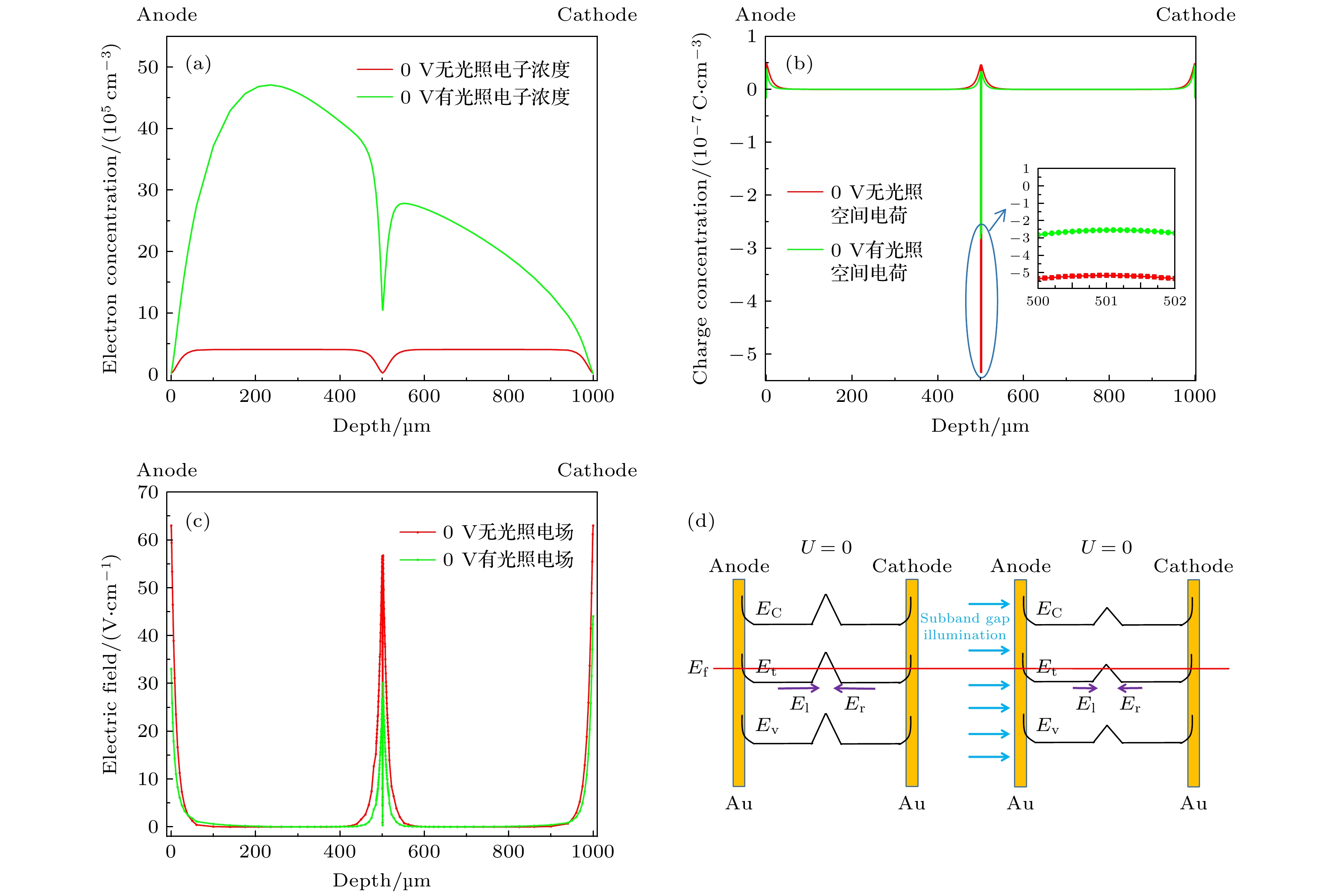
图 2 无偏压下有无光照的Au/CdZnTe/Au器件仿真结果 (a)电子浓度分布; (b)空间电荷分布; (c)电场分布; (d)Au/CdZnTe/Au能带结构图
Fig. 2. Simulation results of Au/CdZnTe/Au device with and without illumination under unbiased voltage: (a) Electron concentration distribution; (b) space charge distribution; (c) electric field distribution; (d) energy band structure diagram of Au/CdZnTe/Au.
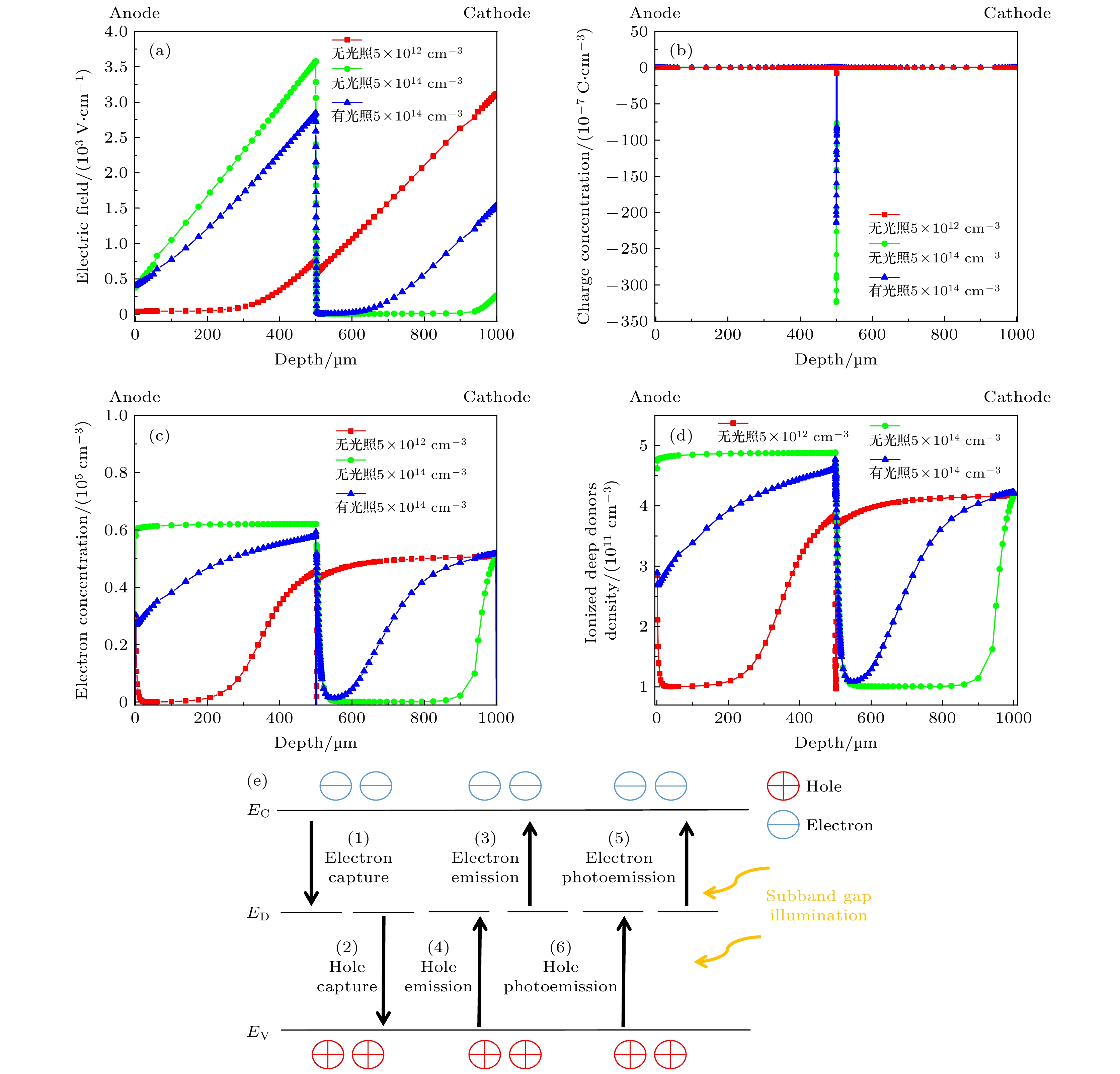
图 3 100 V偏压下有无光照的Au/CdZnTe/Au器件仿真结果 (a)电场分布; (b)空间电荷分布; (c)正空间电荷分布; (d) 深施主电离密度; (e) SRH模型[36-37]
Fig. 3. Simulation results of Au/CdZnTe/Au device with and without illumination under 100 V bias voltage: (a) Electric field distribution; (b) space charge distribution; (c) positive space charge distribution; (d) deep donor ionization density; (e) SRH model[36-37]
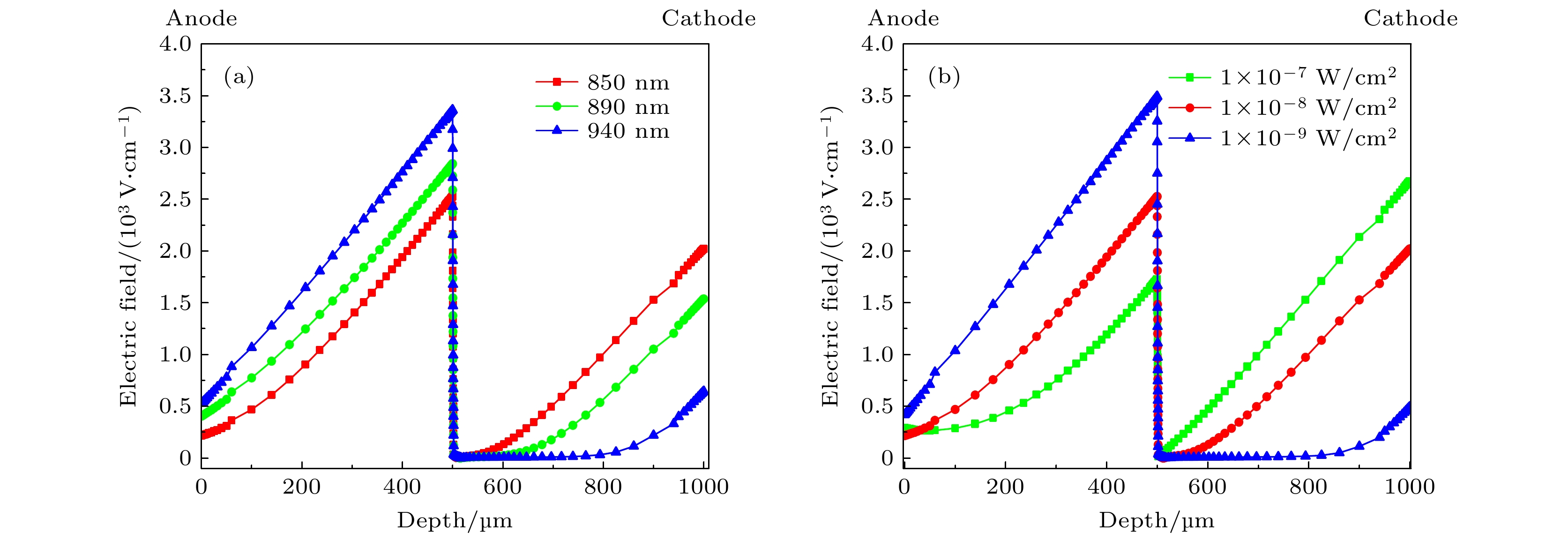
图 4 100 V偏压下的Au/CdZnTe/Au器件仿真结果 (a)不同波长的亚禁带光照下电场分布; (b) 不同光强的亚禁带光照下电场分布
Fig. 4. Simulation results of Au/CdZnTe/Au device under 100 V bias voltage: (a) Electric field distribution under sub-bandgap illumination with different wavelengths; (b) electric field distribution under sub-bandgap illumination with different intensities.
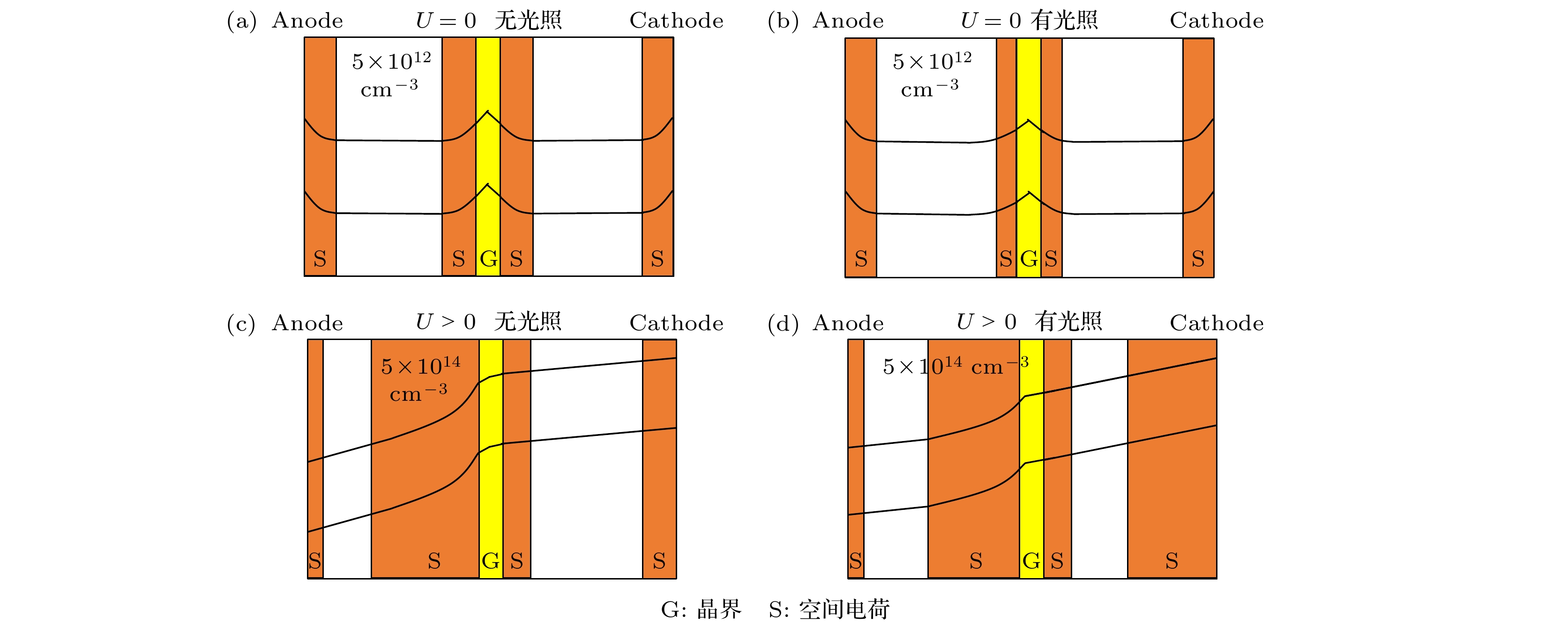
图 5 Au/CdZnTe/Au器件有无光照的能带模型 (a)无偏压下无光照能带模型; (b)无偏压下有光照能带模型 (c) 外加偏压下无光照能带模型(d)外加偏压下有光照能带模型
Fig. 5. Energy band model of Au/CdZnTe/Au device with and without illumination: (a) Energy band model without illumination under unbiased voltage; (b) energy band model with illumination under unbiased voltage ;(c) energy band model without illumination under applied bias voltage; (d) energy band model with illumination under applied bias voltage.
Parameters Value Parameters Value Band gap/eV 1.6 Dielectric constant 10.9 Conduction band density/cm–3 9.14×10¹⁷ Optical recombination rate/(cm3·s–1) 1.5×10⁻¹⁰ Valence band density/cm–3 5.19×10¹⁸ Electronic auger coefficient/(cm6·s–1) 5×10–30 Electron mobility/cm2/(V·s) 1000 Hole Auger coefficient/(cm6·s–1) 1×10–31 Hole mobility/cm2/(V·s) 100 Acceptor band tail state/(cm–3·eV–1) 7.5×10¹⁴ Donor band tail state/(cm–3·eV–1) 7.5×10¹⁴  下载: 导出CSV
表 2 CdZnTe晶体基体能级的基本信息[21]
Table 2. Basic information of the energy levels in the CdZnTe crystal matrix[21].
Level position
/eVType Density
/cm–3Electron capture cross section/cm2 Hole capture cross section/cm2 EV+0.86 Donor 5×10¹¹ 3×10–14 3×10–15
下载: 导出CSV
Level
position
/eVType Density
/cm–3Electron
capture cross
section/cm2Hole capture
cross section/cm2EC – 0.10 Donor 1×10¹² 1.2×10⁻¹⁵ 1.2×10⁻¹⁶ EV + 0.14 Acceptor 1×10¹² 2.5×10⁻¹⁵ 2.5×10⁻¹⁶ EV + 0.75 Acceptor 5×10¹² 3×10–14 3×10–15
下载: 导出CSV
Wavelength/nm Extinction coefficient k Refractive index n Absorption coefficient/cm–1 890 1.417×10⁻⁴ 2.9196 10
下载: 导出CSV
-
[1] Johns P M, Nino J C 2019 J. Appl. Phys. 126 40902
Google Scholar
[2] Kathalingam A, Valanarasu S, Ramesh S, Kim H S, Kim H S 2021 Sol. Energy. 224 923
Google Scholar
[3] 李颖锐, 吴森, 郭玉, 席守智, 符旭, 查钢强, 介万奇 2019 红外与激光工程 48 1016001
Google Scholar
Li Y R, Wu S, Guo Y, Xi S Z, Fu X, Zha G Q, Jie W Q 2019 Infrared Laser Eng. 48 1016001
Google Scholar
[4] Abbene L, Principato F, Gerardi G, Buttacavoli A, Cascio D, Bettelli M, Amade N S, Seller P, Veale M, Fox O, Sawhney K, Zanettini S, Tomarchio E, Zappettini A 2020 J. Synchrotron Radiat. 27 319
Google Scholar
[5] Gao X, Sun H, Yang D, Wangyang P, Zhang C, Zhu X 2020 Vacuum 183 109855
Google Scholar
[6] Chu M, Terterian S, Ting D, Wang C C, Gurgenian H K, Mesropian S 2001 Appl. Phys. Lett. 79 2728
Google Scholar
[7] Carvalho A, Tagantsev A K, Oberg S, Briddon P R, Setter N 2010 Phys. Rev. B 81 075215
Google Scholar
[8] 孙士文, 隋淞印, 何力, 周昌鹤, 虞慧娴, 徐超 2014 红外技术 36 588
Google Scholar
Sun S W, Sui S Y, Li H E, Zhou C H, Yu H X, Xu C 2014 IR. Tech. 36 588
Google Scholar
[9] Parker B H, Stahle C M, Roth D, Babu S, Tueller J 2001 Proc. SPIE. 4507 68
Google Scholar
[10] Zeng D M, Jie W Q, Wang T, Zhou H 2009 J. Cryst. Growth 311 4414
Google Scholar
[11] Markunas J K, Almeida L A, Jacobs R N, Pellegrino J, Qadri S B, Mahadik N, Sanghera J 2010 J. Electron. Mater 39 738
Google Scholar
[12] Bolotnikov A E, Babalola S O, Camarda G S, et al. 2009 IEEE Trans. Nucl. Sci. 56 1775
Google Scholar
[13] Li W, Tkaczyk J E, Andreini K W, Cui J, Zhang T, Williams Y, Harding K G, Chen H, Bindley G, Matyi R J 2009 IEEE Nuclear Science Symposium Conference Record Orlando, USA, October 24–November 1, 2009 p1658
[14] Dong J P, Jie W Q, Yu J Y, Guo R R, Teichert C, Gradwohl K P, Zhang B B, Luo X X, Xi S Z, Xu Y D 2018 Chin. Phys. B. 27 117202
Google Scholar
[15] Prokesch M, Szeles C 2010 US Patent 20100078558 A1
[16] Ivanov V, Dorogov P, Loutchanski A 2011 International Conference on Advancements in Nuclear Instrumentation, Measurement Methods and their Applications Ghent, Belgium, June 6–9, 2011 p1
[17] Washington A L, Teague L C, Duff M C, Burger A, Groza M, Buliga V 2011 J. Appl. Phys 110 073708
Google Scholar
[18] Sik O, Grmela L, Elhadidy H, et al. 2013 J. Instrum. 8 C06005
Google Scholar
[19] Zhang Y Q, Fu L 2018 Mater. Sci. Forum 922 40
Google Scholar
[20] Prokesch M, Szeles C 2007 Phys. Rev. B 75 245204
Google Scholar
[21] Gul R, Roy U N, James R B 2017 J. Appl. Phys. 121 115701
Google Scholar
[22] Zhou Y M, He Y G, Lu A X, Wan Q 2009 Chin. Phys. B 18 3966
Google Scholar
[23] Kong H S, Lee C 1995 J. Appl. Phys. 78 6122
Google Scholar
[24] Kumari K, Avasthi S 2017 IEEE 44th Photovoltaic Specialists Conference Washington, USA, June 25–30, 2017 p251
[25] Hossain F M, Nishii J, Takagi S, Sugiharad T, Ohtomo A, Fukumura T, Koinuma H, Ohno H, Kawasaki M 2004 Phys. E 21 911
Google Scholar
[26] Zhang A, Zhao X R, Duan L B, Liu J M, Zhao J L 2011 Chin. Phys. B 20 057201
Google Scholar
[27] Kim K H, Na Y H, Park Y J, Jung T R, Kim S U, Hong J K 2004 IEEE Trans. Nucl. Sci. 51 3094
Google Scholar
[28] Kim K H, Ahn S Y, An S Y, Hong J K, Yi Y, Kim S U 2007 Curr Appl. Phys. 7 296
Google Scholar
[29] Wei S H, Zhang S B 2002 Phys. Rev. B 66 155211
Google Scholar
[30] Hjelt K, Juvonen M, Tuomi T, Nenonen S, Eissler E E, Bavdaz M 1997 Phys. Status Solidi. 162 747
Google Scholar
[31] Cola A, Farella I 2013 Sensors 13 9414
Google Scholar
[32] Cola A, Farella I, Anni M, Martucci M C 2012 IEEE Trans. Nucl. Sci 59 1569
Google Scholar
[33] Montmorillon L A D, Delaye P, Launay J C, Roosen G 1995 Opt. Mater. 4 233
Google Scholar
[34] Marple D T F 1964 J. Appl. Phys. 35 539
Google Scholar
[35] Schlesinger T E, Toney J E, Yoon H, Lee E Y, Brunett B A, Franks L, James R B 2001 Mater. Sci. Eng. R 32 103
Google Scholar
[36] Hsieh Y K, Card H C 1989 J. Appl. Phys. 65 2409
Google Scholar
[37] Keevers M J, Green M A 1994 J. Appl. Phys. 75 4022
Google Scholar
[38] 徐凌燕 2014 博士学位论文 (西安: 西北工业大学)
Xu L Y 2014 Ph. D. Dissertation (Xian: Northwestern Polytechnical University)

 下载:
下载:
计量
- 文章访问数: 5297
- PDF下载量: 66
- 被引次数: 0
