


-
在众多二维材料中, 过渡金属硫族化合物由于其具有独特的光电特性深受广大研究者喜爱. 近年来, 由二维过渡金属硫族化合物材料与有机半导体结合构建的范德瓦耳斯异质结受到极大的关注. 这种异质结可以利用两者的优势对光电特性等性能进行调控, 为许多基础物理和功能器件的构建提供了研究思路. 本文构建了酞菁铜/二硫化钼(CuPc/MoS2)范德瓦耳斯异质结, 并对其荧光特性进行了表征和分析. 与单层MoS2相比较发现, 引入有机半导体CuPc后, 异质结当中发生了明显的荧光淬灭现象. 通过荧光分析, 该现象可以用引入CuPc后异质结中负三激子与中性激子之比增加来解释. 此外, 通过第一性原理计算分析发现, 引入CuPc会在MoS2的禁带中引入中间带隙态, 使得CuPc与MoS2之间产生非辐射复合, 这同样会导致荧光淬灭的发生. CuPc/MoS2异质结的荧光淬灭现象可以为同类型范德瓦耳斯异质结的光电特性调控研究提供参考和思路.Among two-dimensional (2D) materials, transition metal chalcogenides (TMDs) have attracted much attention due to their unique photoelectric properties. On the other hand, organic molecules have the characteristics of flexibility, wide source, easy fabrication and low cost. The van der Waals heterostructure constructed by the combination of 2D TMDs and organic semiconductors has attracted enormous attention in recent years. When organic semiconductors combine with TMDs to form van der Waals heterostructure, the hybridization of organic molecules could improve the photoelectric properties and other properties by taking the advantages of these two materials, Therefore, the combination of organic semiconductor molecules and TMDs can provide a research platform for designing many basic physics and functional devices and interesting optoelectronic applications. In this work, CuPc/MoS2 van der Waals heterostructure is built, and its photoluminescence (PL) properties are investigated. It is observed that after introducing CuPc, a significant PL quenching phenomenon occurs in the heterostructure compared with the single layer MoS2 and pure CuPc only. After fitting the PL of CuPc/MoS2 heterostructure system and monolayer MoS2 only, the ratio of trion to neutral exciton is clearly increased in the heterostructure. Furthermore, it is found that two mid-gap states D1 and D2 related to the CuPc are introduced into the band gap of MoS2 by first principle calculation. Through the charge density analysis, we find that the D1 state originates from the sp2 bonding state of the C-C bond while the D2 state comes from the anti-bonding state of the N-Cu bond. Meanwhile, the valence band maximum (VBM) and conduction band minimum (CBM) of CuPc/MoS2 heterostructure are derived from the bonding and anti-bonding states of MoS2, respectively. The charge transfer occurs between the mid-gap states of CuPc and MoS2. However, owing to different positions of charge density distribution of CBM, D2, D1 and VBM, the charge pathway is dominated by non-radiation recombination, which cannot give new PL peak in heterostructure. However, this process reduces the number of carriers involved in the direct recombination of MoS2, which leads PL to quench in the heterostructure. This work would be applied to the manipulation of photoelectric characteristics and the design of TMD/organic-based photovoltaic applications.
-
Keywords:
- MoS2 /
- CuPc /
- van der Waals heterostructure /
- photoluminescence
[1] Novoselov K S, Geim A K, Morozov S V, Jiang D, Zhang Y, Dubonos S V, Grigorieva I V, Firsov A A 2004 Science 306 666
 Google Scholar
[2] Mak K F, Lee C, Hone J, Shan J, Heinz T F 2010 Phys. Rev. Lett. 105 136805
Google Scholar
[3] Fabbri F, Rotunno E, Cinquanta E, et al. 2016 Nat. Commun. 7 13044
Google Scholar
[4] Li H, Zhang Q, Yap C C R, Tay B K, Edwin T H T, Olivier A, Baillargeat D 2012 Adv. Funct. Mater. 22 1385
Google Scholar
[5] Amani M, Lien D H, Kiriya D, et al. 2015 Science 350 1065
Google Scholar
[6] Xu M S, Liang T, Shi M M, Chen H Z 2013 Chem. Rev. 113 3766
Google Scholar
[7] Song I, Park C, Choi H C 2015 Rsc. Adv. 5 7495
Google Scholar
[8] Huang Y L, Zheng Y J, Song Z B, Chi D Z, Wee A T S, Quek S Y 2018 Chem. Soc. Rev. 47 3241
Google Scholar
[9] Zhang X N, de Oteyza D G, Wakayama Y, Dosch H 2009 Surf. Sci. 603 3179
Google Scholar
[10] Fan Q P, Li M, Yang P G, Liu Y, Xiao M J, Wang X D, Tan H, Wang Y F, Yang R Q, Zhu W G 2015 Dyes Pigments 116 13
Google Scholar
[11] Li Q F, Liu S, Chen H Z, Li H Y 2016 Chin. Chem. Lett. 27 1421
Google Scholar
[12] Gehring P, Thijssen J M, van der Zant H S J 2019 Nat. Rev. Phys. 1 381
Google Scholar
[13] Aradhya S V, Venkataraman L 2013 Nat. Nanotechnol. 8 399
Google Scholar
[14] Choi J, Zhang H Y, Choi J H 2016 Acs Nano 10 1671
Google Scholar
[15] Zhao H J, Zhao Y B, Song Y X, et al. 2019 Nat. Commun. 10 5589
Google Scholar
[16] Obaidulla S M, Habib M R, Khan Y, Kong Y H, Liang T, Xu M S 2020 Adv. Mater. Interfaces 7 1901197
Google Scholar
[17] Wang S Y, Chen C S, Yu Z H, He Y L, Chen X Y, Wan Q, Shi Y, Zhang D W, Zhou H, Wang X R, Zhou P 2019 Adv. Mater. 31 1806227
Google Scholar
[18] Huang Y, Zhuge F W, Hou J X, Lv L, Luo P, Zhou N, Gan L, Zhai T Y 2018 Acs Nano 12 4062
Google Scholar
[19] Homan S B, Sangwan V K, Balla I, Bergeron H, Weiss E A, Hersam M C 2017 Nano Lett. 17 164
Google Scholar
[20] Park C J, Park H J, Lee J Y, Kim J, Lee C H, Joo J 2018 Acs Appl. Mater. Inter. 10 29848
Google Scholar
[21] Habib M R, Li H F, Kong Y H, Liang T, Obaidulla S M, Xie S, Wang S P, Ma X Y, Su H X, Xu M S 2018 Nanoscale 10 16107
Google Scholar
[22] Khan Y, Obaidulla S M, Habib M R, Kong Y H, Xu M S 2020 Appl. Sur. Sci. 530 147213
Google Scholar
[23] Mouri S, Miyauchi Y, Matsuda K 2013 Nano. Lett. 13 5944
Google Scholar
[24] Kresse G, Furthmuller J 1996 Comp. Mater. Sci. 6 15
Google Scholar
[25] Heyd J, Scuseria G E, Ernzerhof M 2003 J. Chem. Phys. 118 8207
Google Scholar
[26] Choudhury P, Ravavarapu L, Dekle R, Chowdhury S 2017 J. Phys. Chem. C 121 2959
Google Scholar
-
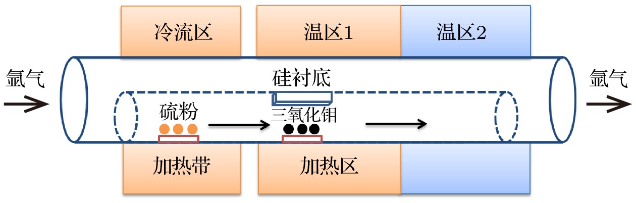
图 1 制备MoS2单晶的CVD装置图
Fig. 1. Schematic illustration of the growth of monolayer MoS2 by CVD.
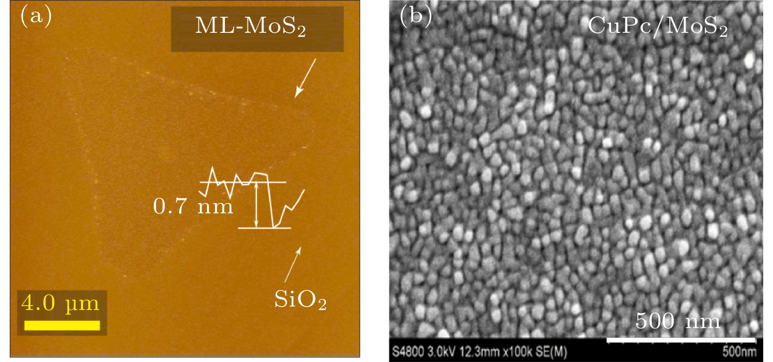
图 2 CuPc/MoS2异质结的形貌表征 (a)单层MoS2的AFM图; (b) CuPc/MoS2异质结的SEM图
Fig. 2. Morphology characterization of CuPc/MoS2 heterostructure system: (a) AFM image of monolayer MoS2; (b) SEM image of CuPc/MoS2 heterostructure.

图 3 CuPc与单层MoS2复合前后的拉曼散射图谱
Fig. 3. Raman scattering spectra of CuPc and monolayer MoS2 (ML-MoS2) before and after recombination.

图 4 CuPc/MoS2异质结的荧光发光图谱 (a) CuPc与单层MoS2复合前后的荧光发光图谱; (b) CuPc/MoS2异质结的荧光面扫描图; (c)单层MoS2的荧光面扫描图
Fig. 4. PL spectra of CuPc/MoS2 heterostructure system: (a) PL spectra of CuPc and monolayer MoS2 before and after recombination; (b) PL mapping image of CuPc/MoS2 heterostructure; (c) PL mapping image of ML-MoS2.

图 5 (a) CuPc/MoS2异质结和(b)单层MoS2的荧光分峰拟合曲线, 其中负三激子A–位置约为1.84 eV, 中性激子A位置约为1.88 eV, B激子位置约为2.01 eV
Fig. 5. PL fitting of (a) CuPc/MoS2 heterostructure and (b) ML-MoS2, where the negative trions A– site is about 1.84 eV, the neutral exciton A site is about 1.88 eV, and the B exciton site is about 2.01 eV.

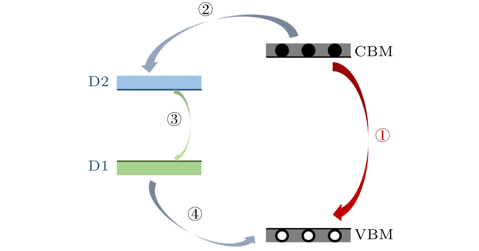
图 6 (a) CuPc/MoS2异质结的分波态密度图; (b)—(e)分别为VBM, D1, D2, CBM的电荷密度分布图
Fig. 6. (a) Partial density of states of CuPc/MoS2 heterostructure; (b)–(e) charge density distribution of VBM, D1, D2, CBM, respectively.
-
[1] Novoselov K S, Geim A K, Morozov S V, Jiang D, Zhang Y, Dubonos S V, Grigorieva I V, Firsov A A 2004 Science 306 666
Google Scholar
[2] Mak K F, Lee C, Hone J, Shan J, Heinz T F 2010 Phys. Rev. Lett. 105 136805
Google Scholar
[3] Fabbri F, Rotunno E, Cinquanta E, et al. 2016 Nat. Commun. 7 13044
Google Scholar
[4] Li H, Zhang Q, Yap C C R, Tay B K, Edwin T H T, Olivier A, Baillargeat D 2012 Adv. Funct. Mater. 22 1385
Google Scholar
[5] Amani M, Lien D H, Kiriya D, et al. 2015 Science 350 1065
Google Scholar
[6] Xu M S, Liang T, Shi M M, Chen H Z 2013 Chem. Rev. 113 3766
Google Scholar
[7] Song I, Park C, Choi H C 2015 Rsc. Adv. 5 7495
Google Scholar
[8] Huang Y L, Zheng Y J, Song Z B, Chi D Z, Wee A T S, Quek S Y 2018 Chem. Soc. Rev. 47 3241
Google Scholar
[9] Zhang X N, de Oteyza D G, Wakayama Y, Dosch H 2009 Surf. Sci. 603 3179
Google Scholar
[10] Fan Q P, Li M, Yang P G, Liu Y, Xiao M J, Wang X D, Tan H, Wang Y F, Yang R Q, Zhu W G 2015 Dyes Pigments 116 13
Google Scholar
[11] Li Q F, Liu S, Chen H Z, Li H Y 2016 Chin. Chem. Lett. 27 1421
Google Scholar
[12] Gehring P, Thijssen J M, van der Zant H S J 2019 Nat. Rev. Phys. 1 381
Google Scholar
[13] Aradhya S V, Venkataraman L 2013 Nat. Nanotechnol. 8 399
Google Scholar
[14] Choi J, Zhang H Y, Choi J H 2016 Acs Nano 10 1671
Google Scholar
[15] Zhao H J, Zhao Y B, Song Y X, et al. 2019 Nat. Commun. 10 5589
Google Scholar
[16] Obaidulla S M, Habib M R, Khan Y, Kong Y H, Liang T, Xu M S 2020 Adv. Mater. Interfaces 7 1901197
Google Scholar
[17] Wang S Y, Chen C S, Yu Z H, He Y L, Chen X Y, Wan Q, Shi Y, Zhang D W, Zhou H, Wang X R, Zhou P 2019 Adv. Mater. 31 1806227
Google Scholar
[18] Huang Y, Zhuge F W, Hou J X, Lv L, Luo P, Zhou N, Gan L, Zhai T Y 2018 Acs Nano 12 4062
Google Scholar
[19] Homan S B, Sangwan V K, Balla I, Bergeron H, Weiss E A, Hersam M C 2017 Nano Lett. 17 164
Google Scholar
[20] Park C J, Park H J, Lee J Y, Kim J, Lee C H, Joo J 2018 Acs Appl. Mater. Inter. 10 29848
Google Scholar
[21] Habib M R, Li H F, Kong Y H, Liang T, Obaidulla S M, Xie S, Wang S P, Ma X Y, Su H X, Xu M S 2018 Nanoscale 10 16107
Google Scholar
[22] Khan Y, Obaidulla S M, Habib M R, Kong Y H, Xu M S 2020 Appl. Sur. Sci. 530 147213
Google Scholar
[23] Mouri S, Miyauchi Y, Matsuda K 2013 Nano. Lett. 13 5944
Google Scholar
[24] Kresse G, Furthmuller J 1996 Comp. Mater. Sci. 6 15
Google Scholar
[25] Heyd J, Scuseria G E, Ernzerhof M 2003 J. Chem. Phys. 118 8207
Google Scholar
[26] Choudhury P, Ravavarapu L, Dekle R, Chowdhury S 2017 J. Phys. Chem. C 121 2959
Google Scholar

 下载:
下载:
计量
- 文章访问数: 6900
- PDF下载量: 213
- 被引次数: 0
