


-
Due to the excellent properties of GaN, such as wide band gap, high electron mobility, high saturation speed, and high breakdown electric field, AlGaN/GaN high electron mobility transistor (HEMT) possesses highly promising applications in the fields of high power, radio frequency, and high temperature applications. However, they are still subjected to the influence of current collapse which strangles its development. Based on the double-pulse technique, the effect of GaN buffer layer trap on the current collapse of AlGaN/GaN HEMT is studied. The results show that the electric field peak at the gate edge is one of the main causes of current collapse. The channel electrons are trapped by the buffer trap under the peak electric field. Because the response speed of the trap in the buffer layer is slow, the channel can not be turned on immediately after the gate voltage has jumped to 0 V, which leads the current to collapse. In this paper, the new structure is proposed by introducing a groove structure in the barrier layer. The channel two-dimensional electron gas is modulated by the groove structure, which influences the channel electric field of AlGaN/GaN HEMT device, reduces the electric field peak at the gate edge, and improves the current collapse effect of the device. Comparing with the traditional AlGaN/GaN HEMT, the inhibition effect of the new device structure on current collapse is increased by 22.30%. The length and height of the groove structure are the critical parameters to affect the new HEMT performance. The optimal parameters of length and hight show that when the length of the groove is 1 μm and the height is 0.01 μm, the current collapse of HEMT and its performance are significantly improved.
-
Keywords:
- AlGaN/GaN /
- high electron mobility transistor /
- current collapse /
- buffer layer trap
[1] Lin Z T, Chen X F, Zhu Y H, Chen X W, Huang L G, Li G Q 2018 IEEE Trans. Electron Dev. 65 5373
 Google Scholar
[2] Zhao L X, Zhu S C, Wu C H, Yang C, Yu Z G, Yang H, Liu L 2016 Sci. China: Phys. Mech. Astron. 59 107301
Google Scholar
[3] Zhao L X, Yu Z G, Sun B, Zhu S C, An P B, Yang C, Liu L, Wang J X, Li J M 2015 Chin. Phy. B 24 068506
Google Scholar
[4] Chen K J, Häberlen O, Lidow A, Tsai C L, Ueda T, Uemoto Y, Wu Y F 2017 IEEE Trans. Electron Dev. 64 779
Google Scholar
[5] 余晨辉, 罗向东, 周文政, 罗庆洲, 刘培生 2012 物理学报 61 207301
Google Scholar
Yu C H, Luo X D, Zhou W Z, Luo Q Z, Liu P S 2012 Acta Phys. Sin. 61 207301
Google Scholar
[6] Radhakrishna U, Choi P, Antoniadis D A 2019 IEEE Trans. Electron Dev. 66 95
Google Scholar
[7] Zhang C, Wang M, Xie B, Wen C P, Wang J Y, Hao Y L, Wu W G, Chen K J, Shen B 2015 IEEE Trans. Electron Dev. 62 2475
Google Scholar
[8] Meneghini M, Rossetto I, Bisi D, Stocco A, Pantellini A, Meneghesso G, Zanoni E 2014 IEEE Trans. Electron Dev. 61 4070
Google Scholar
[9] Miccoli C, Martino V C, Reina S, Rinaudo S 2013 IEEE Electron Dev. Lett. 34 1121
Google Scholar
[10] del Alamo J A, Lee E S 2019 IEEE Trans. Electron Dev. 66 4578
Google Scholar
[11] Gan C L, Sasangka W A, Thompson C V 2019 Electron Devices Technology and Manufacturing Conference Singapore, March 12−15, 2019 p71
[12] 周幸叶, 吕元杰, 谭鑫, 王元刚, 宋旭波, 何泽召, 张志荣, 刘庆彬, 韩婷婷, 房玉龙, 冯志红 2018 物理学报 67 178501
Google Scholar
Zhou X Y, Lv Y J, Tan X, Wang Y G, Song X B, He Z Z, Zhang Z R, Liu Q B, Han T T, Fang Y L, Feng Z H 2018 Acta Phys. Sin. 67 178501
Google Scholar
[13] Ghosh S, Das S, Dinara S M, Bag A, Chakraborty A, Mukhopadhyay P, Jana S K, Biswas D 2018 IEEE Trans. Electron Dev. 65 1333
Google Scholar
[14] Subramani N K, Couvidat J, Hajjar A A, Nallatamby J C, Quéré R 2017 J. Electron Dev. Soc. 5 175
Google Scholar
[15] Vetury R, Zhang N Q, Keller S, Mishra U K 2001 IEEE Trans. Electron Dev. 48 560
Google Scholar
[16] Hwang I, Kim J, Chong S, Choi H S, Hwang S K, Oh J, Shin J K, Chung U I 2013 IEEE Electron Dev. Lett. 34 1494
Google Scholar
[17] Nakano K, Hanawa H, Horio K 2018 Workshop on Wide Bandgap Power Devices and Applications in Asia Xi'an, May 16–18, 2018 p131
[18] Kabemura T, Ueda S, Kawada Y, Horio K 2018 IEEE Trans. Electron Dev. 65 3848
Google Scholar
[19] Wang C H, Ho S Y, Huang J J 2016 IEEE Electron Dev. Lett. 37 74
Google Scholar
[20] Nishitani T, Yamaguchi R, Yamazaki T, Asubar J T, Tokuda H, Kuzuhara M 2018 IEEE International Meeting for Future of Electron Devices Kansai Kyoto, June 21–22, 2018 p1
[21] Koehler A D, Anderson T J, Tadjer M J, Weaver B D, Greenlee J D, Shahin D I, HobartK D, Kub F J 2016 IEEE Electron Dev. Lett. 37 545
Google Scholar
[22] Arakawa Y, Ueno K, Imabeppu H, Kobayashi A, Ohta J, Fujioka H 2017 Appl. Phys. Lett. 110 042103
Google Scholar
[23] Mukherjee K, Darracq F, Curutchet A, Malbert N, Labat N 2017 Microelectron. Reliab. 76 350
-
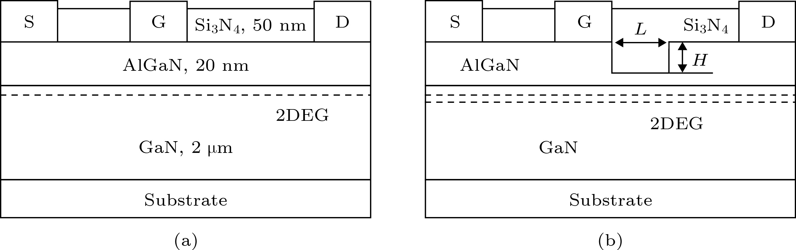
图 1 AlGaN/GaN HEMT结构示意图 (a)传统AlGaN/GaN HEMT; (b)势垒层局部凹槽结构AlGaN/GaN HEMT
Fig. 1. Schematic cross-section of AlGaN/GaN HEMT: (a) Conventional AlGaN/GaN HEMT; (b) AlGaN/GaN HEMT with barrier layer local groove structure.
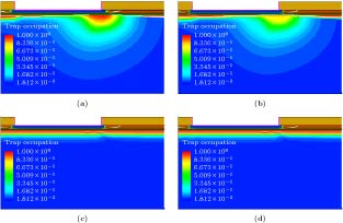
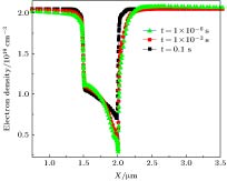
图 5 不同时刻电子占据陷阱的概率分布情况 (a) t = 1 × 10⁻⁶ s; (b) t = 1 × 10⁻³ s; (c) t = 0.1 s; (d)直流情况
Fig. 5. Probability distribution of electron occupying trap at different times: (a) t = 1 × 10⁻⁶ s; (b) t = 1 × 10⁻³ s; (c) t = 0.1 s; (d) direct current.
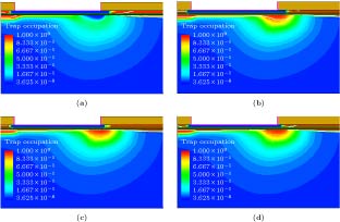
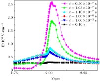
图 6 电子占据陷阱的浓度分布情况 (a) t = 0.5 × 10⁻⁷ s; (b) t = 1.05 × 10⁻⁷ s; (c) t = 1.1 × 10⁻⁷ s; (d) t = 1 × 10⁻⁶ s
Fig. 6. Concentration distribution of electron occupying trap: (a) t = 0.5 × 10⁻⁷ s; (b) t = 1.05 × 10⁻⁷ s; (c) t = 1.1 × 10⁻⁷ s; (d) t = 1 × 10⁻⁶ s.
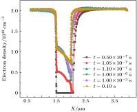
图 8 栅极边缘电子浓度随时间的变化
Fig. 8. Electron concentration at the edge of the gate as a function of time.
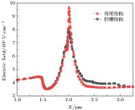
图 9 凹槽结构与传统结构器件的沟道电场分布
Fig. 9. Channel electric field distribution of groove structure and conventional structure device.
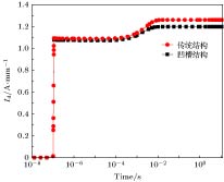
图 10 凹槽结构与传统结构器件的电流崩塌对比
Fig. 10. Comparison of current collapse between groove structure and conventional structural devices.
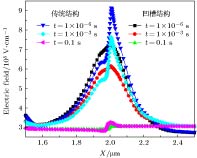
图 11 凹槽结构与传统结构器件在不同时刻的沟道电场分布
Fig. 11. Channel electric field distribution at different times for the groove structure and the conventional structure device.
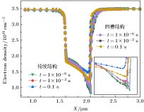
图 12 凹槽结构与传统结构器件在不同时刻沟道电子浓度分布
Fig. 12. Channel electron concentration distribution at different times for the groove structure and the conventional structure device.
-
[1] Lin Z T, Chen X F, Zhu Y H, Chen X W, Huang L G, Li G Q 2018 IEEE Trans. Electron Dev. 65 5373
Google Scholar
[2] Zhao L X, Zhu S C, Wu C H, Yang C, Yu Z G, Yang H, Liu L 2016 Sci. China: Phys. Mech. Astron. 59 107301
Google Scholar
[3] Zhao L X, Yu Z G, Sun B, Zhu S C, An P B, Yang C, Liu L, Wang J X, Li J M 2015 Chin. Phy. B 24 068506
Google Scholar
[4] Chen K J, Häberlen O, Lidow A, Tsai C L, Ueda T, Uemoto Y, Wu Y F 2017 IEEE Trans. Electron Dev. 64 779
Google Scholar
[5] 余晨辉, 罗向东, 周文政, 罗庆洲, 刘培生 2012 物理学报 61 207301
Google Scholar
Yu C H, Luo X D, Zhou W Z, Luo Q Z, Liu P S 2012 Acta Phys. Sin. 61 207301
Google Scholar
[6] Radhakrishna U, Choi P, Antoniadis D A 2019 IEEE Trans. Electron Dev. 66 95
Google Scholar
[7] Zhang C, Wang M, Xie B, Wen C P, Wang J Y, Hao Y L, Wu W G, Chen K J, Shen B 2015 IEEE Trans. Electron Dev. 62 2475
Google Scholar
[8] Meneghini M, Rossetto I, Bisi D, Stocco A, Pantellini A, Meneghesso G, Zanoni E 2014 IEEE Trans. Electron Dev. 61 4070
Google Scholar
[9] Miccoli C, Martino V C, Reina S, Rinaudo S 2013 IEEE Electron Dev. Lett. 34 1121
Google Scholar
[10] del Alamo J A, Lee E S 2019 IEEE Trans. Electron Dev. 66 4578
Google Scholar
[11] Gan C L, Sasangka W A, Thompson C V 2019 Electron Devices Technology and Manufacturing Conference Singapore, March 12−15, 2019 p71
[12] 周幸叶, 吕元杰, 谭鑫, 王元刚, 宋旭波, 何泽召, 张志荣, 刘庆彬, 韩婷婷, 房玉龙, 冯志红 2018 物理学报 67 178501
Google Scholar
Zhou X Y, Lv Y J, Tan X, Wang Y G, Song X B, He Z Z, Zhang Z R, Liu Q B, Han T T, Fang Y L, Feng Z H 2018 Acta Phys. Sin. 67 178501
Google Scholar
[13] Ghosh S, Das S, Dinara S M, Bag A, Chakraborty A, Mukhopadhyay P, Jana S K, Biswas D 2018 IEEE Trans. Electron Dev. 65 1333
Google Scholar
[14] Subramani N K, Couvidat J, Hajjar A A, Nallatamby J C, Quéré R 2017 J. Electron Dev. Soc. 5 175
Google Scholar
[15] Vetury R, Zhang N Q, Keller S, Mishra U K 2001 IEEE Trans. Electron Dev. 48 560
Google Scholar
[16] Hwang I, Kim J, Chong S, Choi H S, Hwang S K, Oh J, Shin J K, Chung U I 2013 IEEE Electron Dev. Lett. 34 1494
Google Scholar
[17] Nakano K, Hanawa H, Horio K 2018 Workshop on Wide Bandgap Power Devices and Applications in Asia Xi'an, May 16–18, 2018 p131
[18] Kabemura T, Ueda S, Kawada Y, Horio K 2018 IEEE Trans. Electron Dev. 65 3848
Google Scholar
[19] Wang C H, Ho S Y, Huang J J 2016 IEEE Electron Dev. Lett. 37 74
Google Scholar
[20] Nishitani T, Yamaguchi R, Yamazaki T, Asubar J T, Tokuda H, Kuzuhara M 2018 IEEE International Meeting for Future of Electron Devices Kansai Kyoto, June 21–22, 2018 p1
[21] Koehler A D, Anderson T J, Tadjer M J, Weaver B D, Greenlee J D, Shahin D I, HobartK D, Kub F J 2016 IEEE Electron Dev. Lett. 37 545
Google Scholar
[22] Arakawa Y, Ueno K, Imabeppu H, Kobayashi A, Ohta J, Fujioka H 2017 Appl. Phys. Lett. 110 042103
Google Scholar
[23] Mukherjee K, Darracq F, Curutchet A, Malbert N, Labat N 2017 Microelectron. Reliab. 76 350

 下载:
下载:

计量
- 文章访问数: 14941
- PDF下载量: 197
- 被引次数: 0
