


-
氧化镓(Ga2O3)薄膜在功率器件以及紫外探测等领域中具有重要的应用潜力, 而实现高质量薄膜制备则是其中的关键. 本文在蓝宝石衬底上物理溅射生长外延Ga2O3层, 因采用引入籽晶层的方法提供了人为成核点而使得外延层结晶质量获得明显改善. 实验发现该外延层薄膜的生长中随着功率增加, 晶粒团聚到一定尺寸后出现裂解现象. 这一物理机制归因于大功率下溅射粒子在生长晶面上扩散携带的能量过大导致粒子碰撞次数增多. 文中生长的外延层为
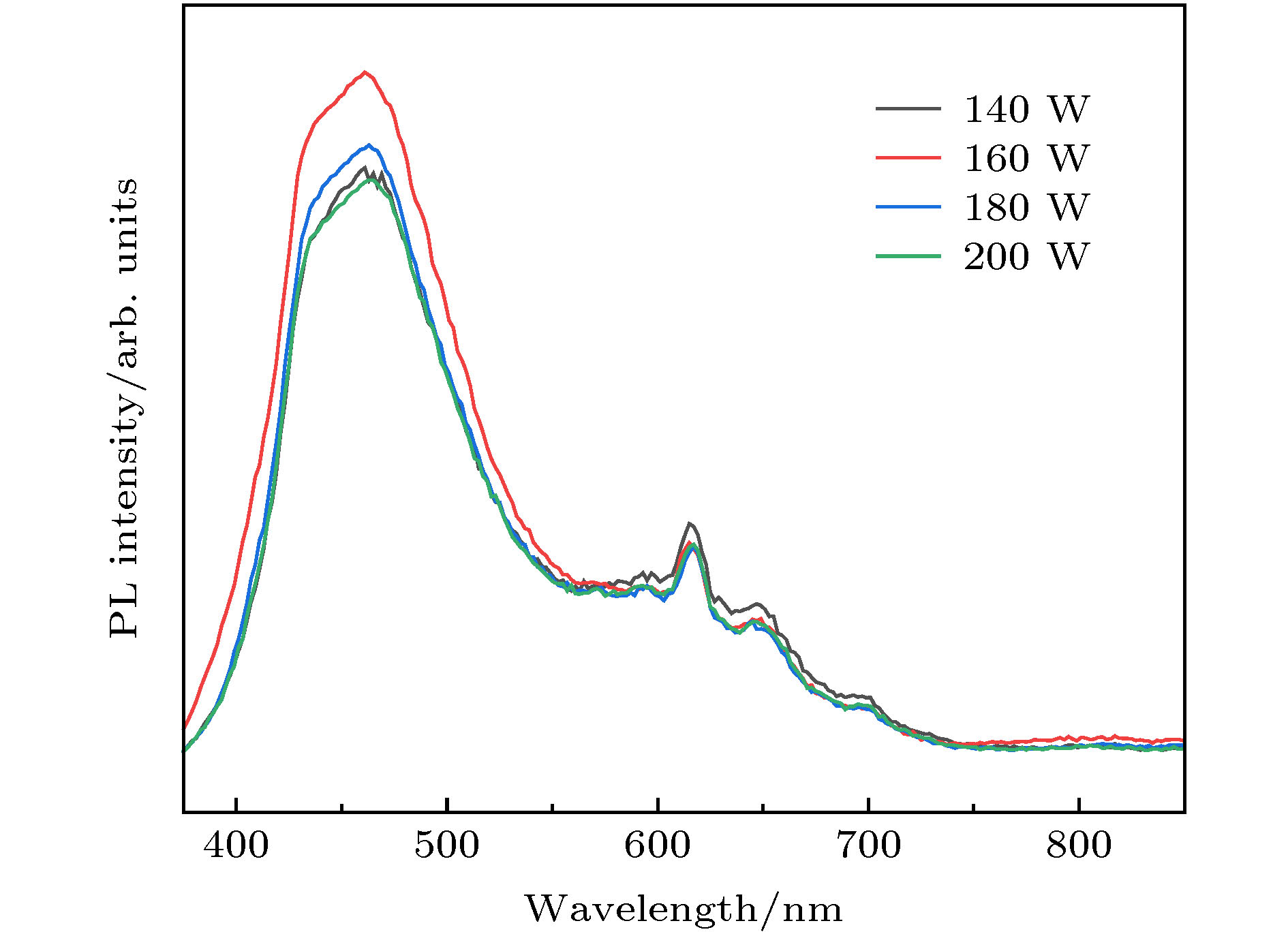
$ \left( {\bar 2\;0\;1} \right)$ 晶面取向的β型Ga2O3薄膜, 厚度在202.4—292.3 nm之间, 薄膜在450—800 nm范围可见光波段的透射率约为90%, 吸收边随着功率的增加先蓝移后红移, 带隙约为4.81—4.96 eV. 光致发光光谱分析表明, 该外延层薄膜在460 nm处产生蓝色发光. 本文发现溅射功率为160 W时引入籽晶层生长的β-Ga2O3薄膜具有最佳的结晶质量, 这一方法将为高质量β-Ga2O3薄膜的可控生长提供有益参考.Gallium oxide (Ga2O3) thin films have great potential applications in UV detectors and power devices; the preparation of high-quality films still needs further studying. In this paper, the Ga2O3 epitaxial thin films are grown by physical sputtering on the seed layer under different power conditions, and the growth mechanism of Ga2O3 epitaxial films are investigated. The introduction of a seed layer provides an artificial nucleation point, which effectively alleviates the lattice mismatch between sapphire substrate and Ga2O3 epitaxial films. thereby improving the quality of the epitaxial layer significantly. Through experiments, it is found that as the power of the epitaxial layer film increases during the growth, the crystal grains agglomerate to a certain size and crack. This physical phenomenon is attributed to the fact that the energy carried by sputtered particles is too large under the condition of high power, which leads the number of particle collisions to increase when they diffuse on the growing crystal surface. The X-ray diffraction, atomic force microscope, field emission scanning electron microscope, ultraviolet spectrophotometer, and photo-luminescence spectrum are used to characterize the structure, morphology, and optical properties of the deposited Ga2O3 thin film. The results show that the epitaxial films are β-Ga2O3 with$ \left( {\bar 2\;0\;1} \right)$ orientation, and the thickness values of thin films are between 202.4 and 292.3 nm. Comparing with the Ga2O3 thin films grown directly on sapphire, the surface particle size increases significantly and the crystal quality is improved greatly under the condition of seed layer. The surface roughness is still maintained at a lower value reaching the device preparation standard. All Ga2O3 epitaxial films show that they have the high transmittance of about 90% in the visible light region (450-800 nm) and drop sharply at 350-400 nm. As the power increases, the absorption edge is blue-shifted and then red-shifted. The estimated band gap is about 4.81-4.96 eV. The PL spectra show that thin films produce blue emission only at 460 nm. It is found that the Ga2O3 films grown on seed layer at a sputtering power of 160 W have the excellent crystal quality. The results should be helpful in implementing the controllable preparation of high-quality β-Ga2O3 thin films in the future.-
Keywords:
- β-Ga2 O3 /
- epitaxy /
- wide band-gap semiconductor /
- magnetron sputtering
[1] Onuma T, Saito S, Sasaki K, Masui T, Yamaguchi T, Honda T, Higashiwaki M 2015 Jpn. J. Appl. Phys. 54 112601
 Google Scholar
[2] Higashiwaki M, Sasaki K, Kuramata A, Masui T, Yamakoshi S 2014 Phys. Status Solidi A 211 21
Google Scholar
[3] Pearton S J, Yang J C, Cary P H, Ren F, Kim J, Tadjer M J, Mastro M A 2018 Appl. Phys. Rev. 5 011301
Google Scholar
[4] Zinkevich M, Aldinger F 2004 J. Am. Ceram. Soc. 87 683
Google Scholar
[5] Playford H Y, Hannon A C, Barney E R, Walton R I 2013 Chem. Eur. J. 19 2803
Google Scholar
[6] Gottschalch V, Merker S, Blaurock S, Kneiss M, Teschner U 2019 J. Cryst. Growth 510 76
Google Scholar
[7] Ghose S, Rahman S 2016 J. Vac. Sci. Technol., B 34 02L109
Google Scholar
[8] Shi F F, Han J, Xing Y H, Li J S, Zhang L, He T, Li T, Deng X G, Zhang X D, Zhang B S 2019 Mater. Lett. 237 105
Google Scholar
[9] Higashiwaki M, Sasaki K, Kuramata A, Masui T, Yamakoshi S 2012 Appl. Phys. Lett. 100 013504
Google Scholar
[10] Han S, Huang X L, Fang M Z, Zhao W G, Xu S J, Zhu D, Xu W Y, Fang M, Liu W J, Cao P J, Lu Y M 2019 J. Mater. Chem. C 7 11834
Google Scholar
[11] Kang H C 2014 Mater. Lett. 119 123
Google Scholar
[12] Kalarickal N K, Xia Z B, McGlone J, Krishnamoorthy S, Moore W, Brenner M, Arehart A R, Ringel S A, Rajan S 2019 Appl. Phys. Lett. 115 152106
Google Scholar
[13] Orita M, Ohta H, Hirano M 2000 Appl. Phys. Lett. 77 4166
Google Scholar
[14] Cai Y C, Zhang K, Feng Q, Zuo Y, Hu Z Z, Feng Z Q, Zhou H, Lu X L, Zhang C F, Tang W H, Zhang J C, Hao Y 2018 Opt. Mater. Express 8 3506
Google Scholar
[15] Roberts J W, Jarman J C, Johnstone D N, Midgley P A, Chalker P R, Oliver R A, Massabuau F C 2018 J. Cryst. Growth 487 23
Google Scholar
[16] Joishi C, Rafique S, Xia Z B, Han L, Krishnamoorthy S, Zhang Y W, Lodha S, Zhao H P, Rajan S 2018 Appl. Phys. Express 11 031101
Google Scholar
[17] Mi W, Ma J, Luan C, Xiao H D 2014 J. Lumin. 146 1
Google Scholar
[18] Li S F, Jiao S J, Wang D B, Gao S Y, Wang J Z 2018 J. Alloys Compd. 753 186
Google Scholar
[19] Wu J W, Mi W, Yang Z C, Chen Y T, Li P J, Zhao J S, Zhang K L, Zhang X C, Luan C B 2019 Vacuum 167 6
Google Scholar
[20] Li Z, An Z Y, Xu Y, Cheng Y L, Cheng Y N, Chen D Z, Feng Q, Xu S R, Zhang J C, Zhang C F, Hao Y 2019 J. Mater. Sci. 54 10335
Google Scholar
[21] 马海林, 苏庆 2014 物理学报 63 116701
Google Scholar
Ma H L, Su Q 2014 Acta. Phys. Sin. 63 116701
Google Scholar
[22] Chen Y P, Liang H W, Xia X C, Tao P C, Shen R S, Liu Y, Feng Y B, Zheng Y H, Li X N, Du G T 2015 J. Mater. Sci.- Mater. Electron. 26 3231
Google Scholar
[23] Nakagomi S, Kokubun Y 2012 J. Cryst. Growth 349 12
Google Scholar
[24] Ghose S, Rahman S, Hong L, Rojas-Ramirez J S, Jin H, Park K, Klie R, Droopad R 2017 J. Appl. Phys. 122 095302
Google Scholar
[25] Jiao S J, Lu H L, Wang X H, Nie Y Y, Wang D B, Gao S Y, Wang J Z 2019 ECS J. Solid State Sci. 8 Q3086
Google Scholar
[26] 刘浩, 邓宏, 韦敏, 于永斌, 陈文宇 2015 发光学报 36 906
Google Scholar
Liu H, Deng H, Wei M, Yu Y B, Chen W Y 2015 Chin. J. Lumin. 36 906
Google Scholar
[27] Liao Y K, Jiao S J, Li S F, Wang J Z, Wang D B, Gao S Y, Yu Q J, Li H T 2018 Crystengcomm 20 133
Google Scholar
[28] Oanh V T K, Lee D U, Kim E K 2019 J. Alloys Compd. 806 874
Google Scholar
[29] Hu D Q, Zhuang S W, Ma Z Z, Dong X, Du G T, Zhang B L, Zhang Y T, Yin J Z 2017 J. Mater. Sci.- Mater. Electron. 28 10997
Google Scholar
[30] Cheng Y, Yang K, Peng Y, Yin Y, Chen J X, Jing B, Liang H W, Du G T 2013 J. Mater. Sci.-Mater. Electron. 24 5122
Google Scholar
[31] 马腾宇, 李万俊, 何先旺, 胡慧, 黄利娟, 张红, 熊元强, 李泓霖, 叶利娟, 孔春阳 2020 物理学报 69 108102
Google Scholar
Ma T Y, Li W J, He X W, Hu H, Huang L J, Zhang H, Xiong Y Q, Li H L, Ye L J, Kong C Y 2020 Acta Phys. Sin. 69 108102
Google Scholar
-
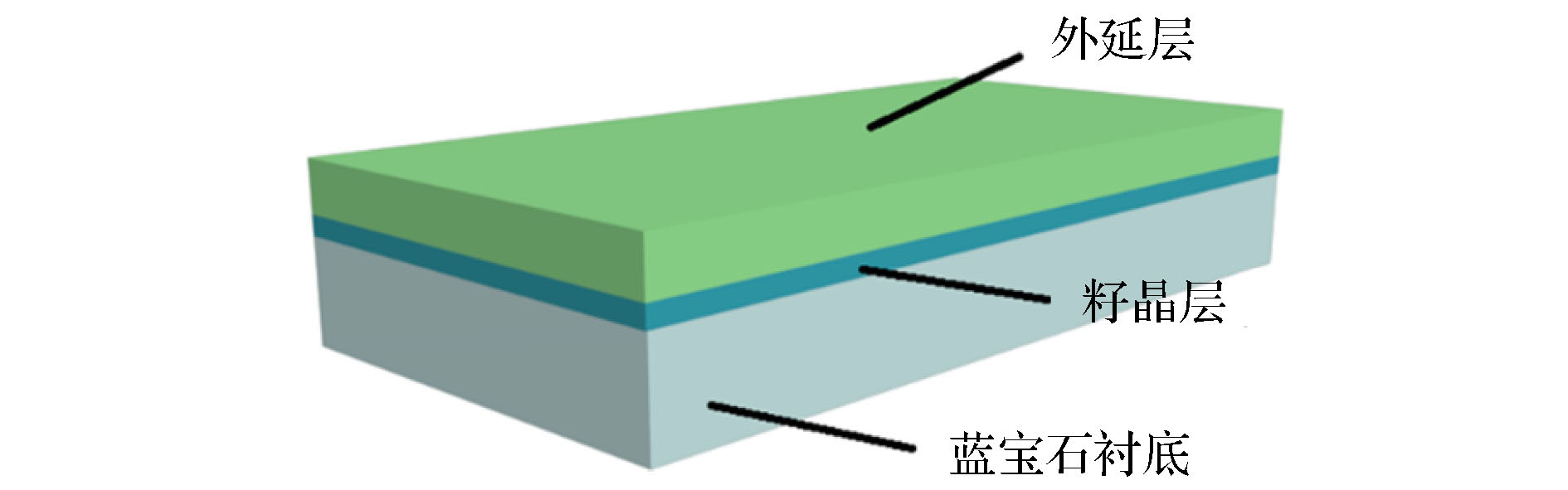
图 1 蓝宝石衬底上Ga2O3籽晶层-外延层薄膜系统结构示意图
Fig. 1. Structure diagram of Ga2O3 seed layer-epitaxial layer.

图 2 不同条件下生长的Ga2O3薄膜AFM扫描图及尺寸估算与RMS折线图 (a)无籽晶层140 W溅射生长; (b)籽晶层上140 W溅射生长; (c)籽晶层上160 W溅射生长; (d)籽晶层上180 W溅射生长; (e)籽晶层上200 W溅射生长; (f) 尺寸估算与RMS折线图
Fig. 2. AFM scans of Ga2O3 thin films grown under different conditions, particle size and RMS lines chart: (a) 140 W sputter growth without seed layer; (b) 140 W sputter growth on seed layer; (c) 160 W sputter growth on the seed layer; (d) 180 W sputter growth on the seed layer; (e) 200 W sputter growth on the seed layer; (f) particle size and RMS lines chart.

图 3 (a) 以不同溅射功率沉积的β-Ga2O3薄膜的XRD图谱; (b) FWHM以及平均晶粒尺寸分布图
Fig. 3. (a) XRD pattern of β-Ga2 O3 thin films deposited at diffreent sputtering power; (b) FWHM and average grain size distribution.
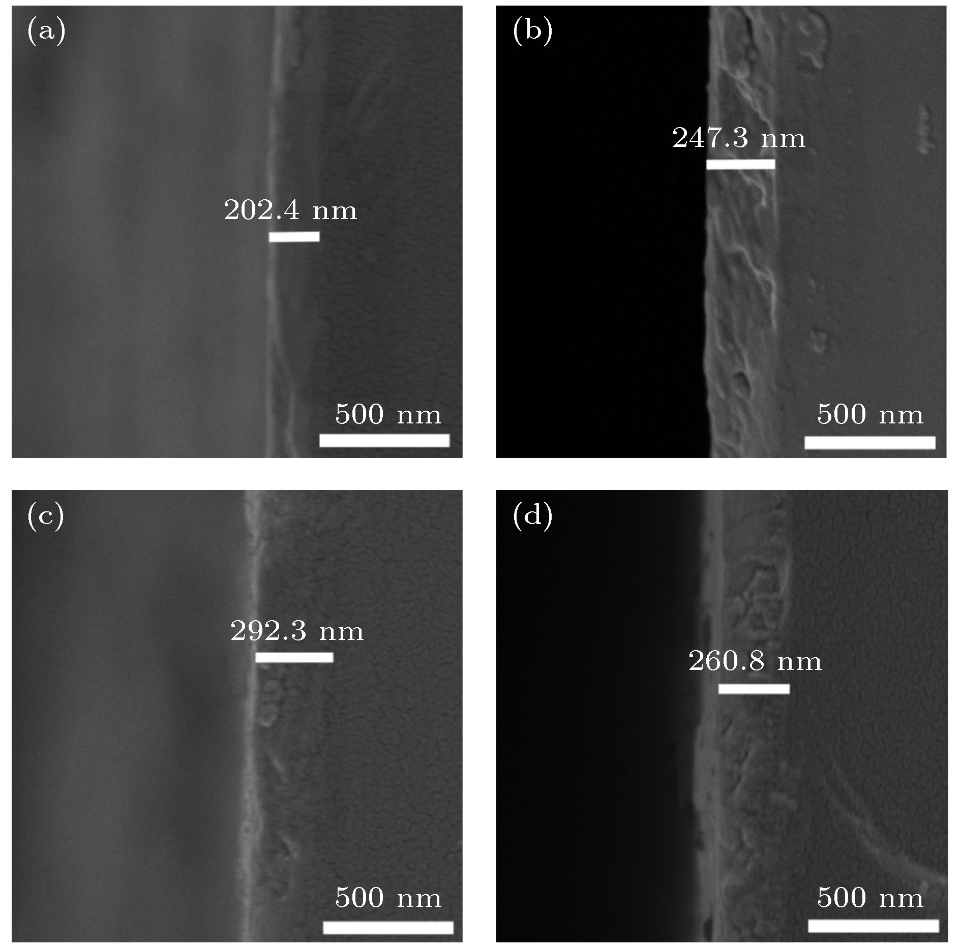
图 4 籽晶层上使用不同功率生长的β-Ga2O3薄膜SEM截面扫描图 (a) 140 W; (b) 160 W; (c) 180 W; (d) 200 W
Fig. 4. SEM cross-section scan of β-Ga2 O3 thin film grown on seed layer with different power: (a) 140 W; (b) 160 W; (c) 180 W; (d) 200 W.

图 5 (a) β-Ga2O3薄膜的透射光谱; (b) (αhν)2~hν曲线图
Fig. 5. (a) Optical transmittance spectra for β-Ga2O3 films; (b) the plot of (αhν)2~hν.
-
[1] Onuma T, Saito S, Sasaki K, Masui T, Yamaguchi T, Honda T, Higashiwaki M 2015 Jpn. J. Appl. Phys. 54 112601
Google Scholar
[2] Higashiwaki M, Sasaki K, Kuramata A, Masui T, Yamakoshi S 2014 Phys. Status Solidi A 211 21
Google Scholar
[3] Pearton S J, Yang J C, Cary P H, Ren F, Kim J, Tadjer M J, Mastro M A 2018 Appl. Phys. Rev. 5 011301
Google Scholar
[4] Zinkevich M, Aldinger F 2004 J. Am. Ceram. Soc. 87 683
Google Scholar
[5] Playford H Y, Hannon A C, Barney E R, Walton R I 2013 Chem. Eur. J. 19 2803
Google Scholar
[6] Gottschalch V, Merker S, Blaurock S, Kneiss M, Teschner U 2019 J. Cryst. Growth 510 76
Google Scholar
[7] Ghose S, Rahman S 2016 J. Vac. Sci. Technol., B 34 02L109
Google Scholar
[8] Shi F F, Han J, Xing Y H, Li J S, Zhang L, He T, Li T, Deng X G, Zhang X D, Zhang B S 2019 Mater. Lett. 237 105
Google Scholar
[9] Higashiwaki M, Sasaki K, Kuramata A, Masui T, Yamakoshi S 2012 Appl. Phys. Lett. 100 013504
Google Scholar
[10] Han S, Huang X L, Fang M Z, Zhao W G, Xu S J, Zhu D, Xu W Y, Fang M, Liu W J, Cao P J, Lu Y M 2019 J. Mater. Chem. C 7 11834
Google Scholar
[11] Kang H C 2014 Mater. Lett. 119 123
Google Scholar
[12] Kalarickal N K, Xia Z B, McGlone J, Krishnamoorthy S, Moore W, Brenner M, Arehart A R, Ringel S A, Rajan S 2019 Appl. Phys. Lett. 115 152106
Google Scholar
[13] Orita M, Ohta H, Hirano M 2000 Appl. Phys. Lett. 77 4166
Google Scholar
[14] Cai Y C, Zhang K, Feng Q, Zuo Y, Hu Z Z, Feng Z Q, Zhou H, Lu X L, Zhang C F, Tang W H, Zhang J C, Hao Y 2018 Opt. Mater. Express 8 3506
Google Scholar
[15] Roberts J W, Jarman J C, Johnstone D N, Midgley P A, Chalker P R, Oliver R A, Massabuau F C 2018 J. Cryst. Growth 487 23
Google Scholar
[16] Joishi C, Rafique S, Xia Z B, Han L, Krishnamoorthy S, Zhang Y W, Lodha S, Zhao H P, Rajan S 2018 Appl. Phys. Express 11 031101
Google Scholar
[17] Mi W, Ma J, Luan C, Xiao H D 2014 J. Lumin. 146 1
Google Scholar
[18] Li S F, Jiao S J, Wang D B, Gao S Y, Wang J Z 2018 J. Alloys Compd. 753 186
Google Scholar
[19] Wu J W, Mi W, Yang Z C, Chen Y T, Li P J, Zhao J S, Zhang K L, Zhang X C, Luan C B 2019 Vacuum 167 6
Google Scholar
[20] Li Z, An Z Y, Xu Y, Cheng Y L, Cheng Y N, Chen D Z, Feng Q, Xu S R, Zhang J C, Zhang C F, Hao Y 2019 J. Mater. Sci. 54 10335
Google Scholar
[21] 马海林, 苏庆 2014 物理学报 63 116701
Google Scholar
Ma H L, Su Q 2014 Acta. Phys. Sin. 63 116701
Google Scholar
[22] Chen Y P, Liang H W, Xia X C, Tao P C, Shen R S, Liu Y, Feng Y B, Zheng Y H, Li X N, Du G T 2015 J. Mater. Sci.- Mater. Electron. 26 3231
Google Scholar
[23] Nakagomi S, Kokubun Y 2012 J. Cryst. Growth 349 12
Google Scholar
[24] Ghose S, Rahman S, Hong L, Rojas-Ramirez J S, Jin H, Park K, Klie R, Droopad R 2017 J. Appl. Phys. 122 095302
Google Scholar
[25] Jiao S J, Lu H L, Wang X H, Nie Y Y, Wang D B, Gao S Y, Wang J Z 2019 ECS J. Solid State Sci. 8 Q3086
Google Scholar
[26] 刘浩, 邓宏, 韦敏, 于永斌, 陈文宇 2015 发光学报 36 906
Google Scholar
Liu H, Deng H, Wei M, Yu Y B, Chen W Y 2015 Chin. J. Lumin. 36 906
Google Scholar
[27] Liao Y K, Jiao S J, Li S F, Wang J Z, Wang D B, Gao S Y, Yu Q J, Li H T 2018 Crystengcomm 20 133
Google Scholar
[28] Oanh V T K, Lee D U, Kim E K 2019 J. Alloys Compd. 806 874
Google Scholar
[29] Hu D Q, Zhuang S W, Ma Z Z, Dong X, Du G T, Zhang B L, Zhang Y T, Yin J Z 2017 J. Mater. Sci.- Mater. Electron. 28 10997
Google Scholar
[30] Cheng Y, Yang K, Peng Y, Yin Y, Chen J X, Jing B, Liang H W, Du G T 2013 J. Mater. Sci.-Mater. Electron. 24 5122
Google Scholar
[31] 马腾宇, 李万俊, 何先旺, 胡慧, 黄利娟, 张红, 熊元强, 李泓霖, 叶利娟, 孔春阳 2020 物理学报 69 108102
Google Scholar
Ma T Y, Li W J, He X W, Hu H, Huang L J, Zhang H, Xiong Y Q, Li H L, Ye L J, Kong C Y 2020 Acta Phys. Sin. 69 108102
Google Scholar


 下载:
下载:
计量
- 文章访问数: 10779
- PDF下载量: 228
- 被引次数: 0
