-
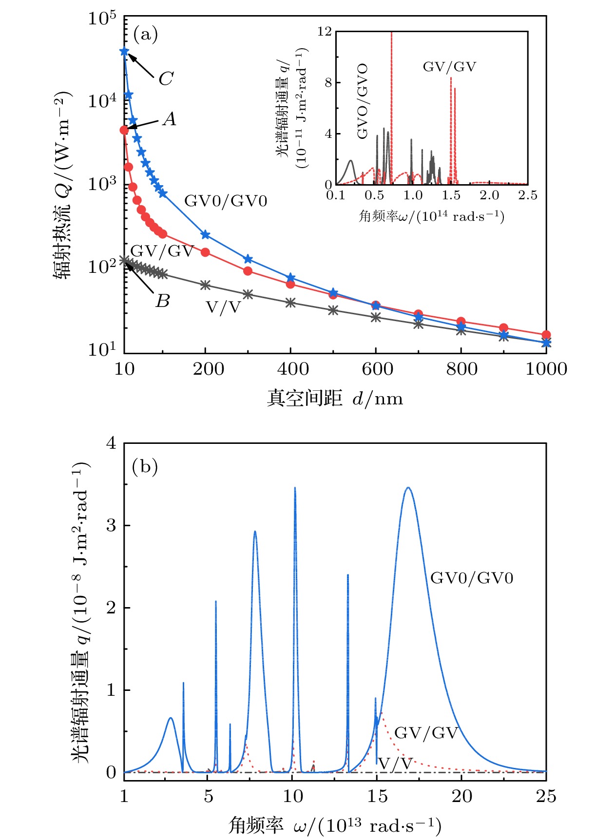
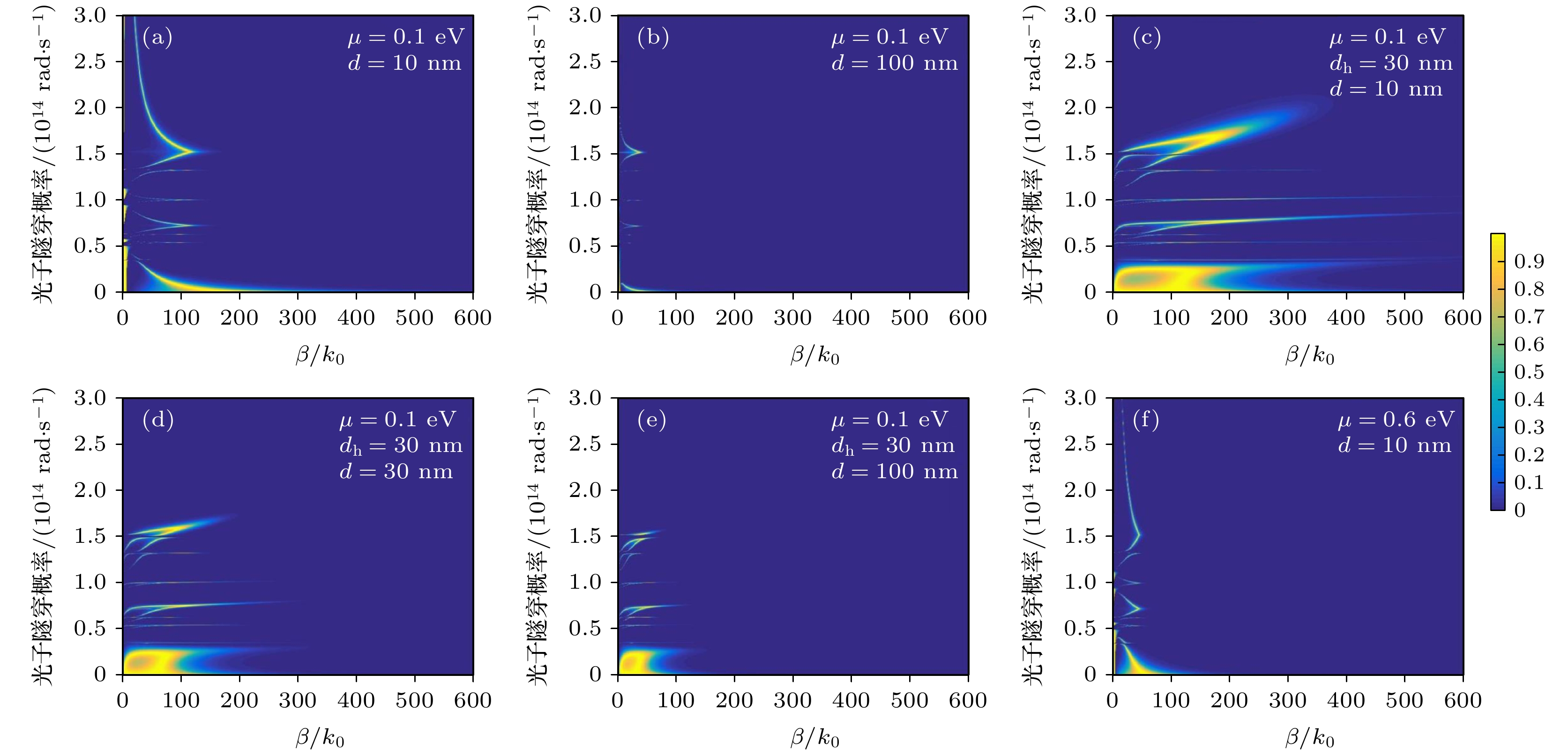
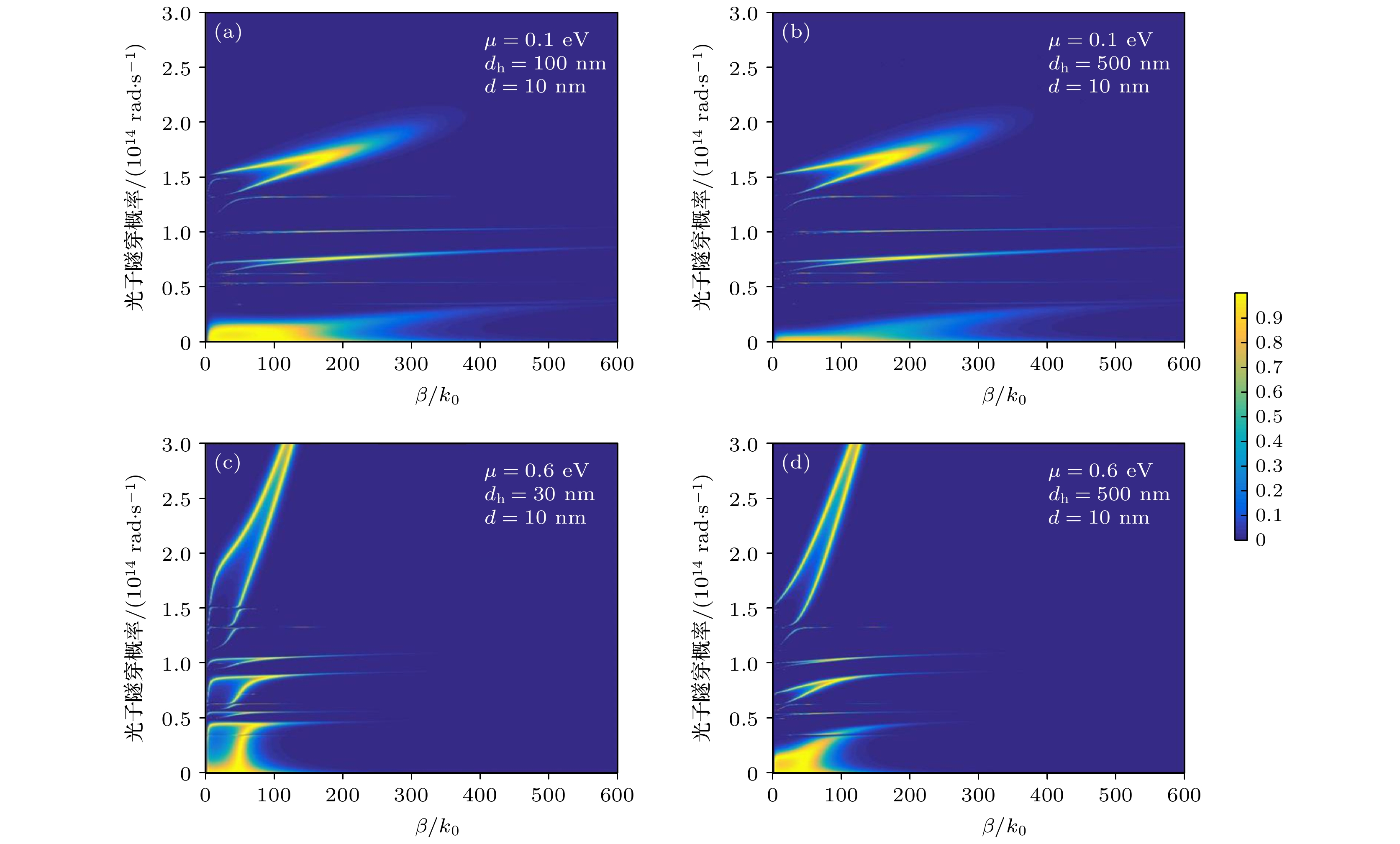
本文基于涨落耗散定理和并矢格林函数求解麦克斯韦方程来研究两个半无限大平板的近场热辐射净热流, 提出了两个半无限大块状二氧化钒组成的V/V结构、石墨烯覆盖两个半无限大块状二氧化钒组成的GV/GV结构和石墨烯覆盖VO2薄膜组成的GV0/GV0结构, 深入研究了这三种结构中二氧化钒与石墨烯间的近场热辐射, 并分析了真空间距、二氧化钒薄膜厚度和石墨烯化学势等物理参量变化对近场热辐射的影响. 研究表明: 三种结构的近场热辐射均随间距增大而减小; 在真空间距为10 nm时, 由石墨烯覆盖的GV/GV结构的近场辐射热流比无石墨烯覆盖的V/V结构增强35倍, 耦合效果最好的是GV0/GV0结构, 该结构的近场辐射热流比GV/GV结构增强8.6倍; 在GV0/GV0结构中, 当二氧化钒薄膜厚度为30 nm时, 石墨烯化学势从0.1 eV增加到0.6 eV辐射热流会减小3.3倍. 本文系统研究了二氧化钒与石墨烯间相互耦合的近场热辐射, 对相关结构的近场热辐射实验和实际应用具有理论指导意义.Near-field thermal radiation refers to the radiation produced by two radiators in a narrow gap that is smaller than the characteristic wavelength. The studies of near-field thermal radiation began in the 1960s and 1970s. Some researchers have reported that near-filed thermal radiation can be enhanced by orders of magnitude higher than that of far-field radiation by photon tunneling and surface polariton. With the development and application of nanotechnology, the near-field heat radiation has developed into a research hotspot in the field of heat radiation. Recent studies have shown that the properties of near-field thermal radiation can be enhanced by optimizing the structures of radiators (covered by two-dimensional (2D) materials, such as graphene and black phosphorus), choosing radiation materials (hexagonal boron nitride, silicon dioxide, vanadium dioxide), and selecting appropriate physical parameters (chemical potential, vacuum distance, film thickness) of the radiator materials. According to the fluctuation dissipation theory and by solving the Maxwell equation and the green's function, in this article we report the near-field thermal radiation of the two half-infinite flats, including vanadium dioxide V/V, vanadium dioxide covered by graphene GV/GV and vanadium dioxide film covered by graphene GV0/GV0. The near-field thermal radiations in these structures are influenced by physical parameters, such as vacuum spacing, thickness of vanadium dioxide film and chemical potential of graphene. The results show that near-field thermal radiation of GV0/GV0 (38088.43 W/m2) is 8.6 times stronger than that of GV/GV (4426.73 W/m2, vacuum distance is 10 nm, chemical potential is 0.1 eV), and near-field thermal radiation of GV/GV (4426.73 W/m2) is 35 times stronger than that of V/V (127.21 W/m2, vacuum distance is 10 nm, chemical potential is 0.1 eV). For these three structures, thermal radiation decreases gradually by widening the vacuum distance. Moreover, thermal radiation also decreases by thickening vanadium dioxide film. While thermal radiation of GV0/GV0 decreases 3.34 times as chemical potential of graphene increases from 0.1 (38088.43 W/m2) to 0.6 eV (11399.80 W/m2). In this paper, the near-field heat radiation between vanadium dioxide and graphene is systematically investigated, which will give the guidance in the relevant experiment and practical applications of near-field heat radiation between vanadium dioxide and graphene.
-
Keywords:
- near-field thermal radiation /
- film thickness /
- graphene /
- vanadium dioxide
[1] 刘扬, 潘登, 陈文, 王文强, 沈昊, 徐红星 2020 物理学报 69 036501
 Google Scholar
Liu Y, Pan D, Chen W, Wang W Q, Shen H, Xu H X 2020 Acta Phys. Sin. 69 036501
 Google Scholar
[2] ShiK Z, Bao F L, He S L 2017 ACS photonics 4 971
 Google Scholar
[3] Ilic O, Jablan M, Joannopoulos J D, Celanovic I, Buljan H 2012 Phys. Rev. B 85 155422
 Google Scholar
[4] Ge L X, Xu Z J, Cang Y P, Gong K 2019 Opt. Express 27 A1109
 Google Scholar
[5] 赵启梅 2018 硕士学位论文 (南昌: 南昌大学)
Zhao Q M 2018 M. A. Thesis (Nanchang: Nanchang University) (in Chinese)
[6] Zhao B, Guizal B, Zhang Z M, Fan S H, Antezza M 2017 Phys. Rev. B 95 245437
 Google Scholar
[7] Lim M, Lee S S, Lee B J 2013 Opt. Express 21 22173
 Google Scholar
[8] Qazilbash M M, Brehm M, Andreev G O, Frenzel P C H, Chae B G, Kim B G, Yun S j, Kim H T, Balatsky A V, Shpyrko O G, Maple M B, Keilmann F, Basov D N 2009 Phys. Rev. B 79 075107
 Google Scholar
[9] Manish K, Sunita R, Hyun H L 2019 J. Korean Phys. Soc. 75 519
 Google Scholar
[10] Li S Y, Niklasson G A, Granqvist C G 2014 J. Appl. Phys. 115 053513
 Google Scholar
[11] Choi H S, Ahn J S, Jung J H, Noh T W 1996 Phys. Rev. B 54 4621
 Google Scholar
[12] Van Zwol P J, Joulain K, Abdallah P B, Chevrier J 2011 Phys. Rev. B 83 201404(R
 Google Scholar
[13] Van Zwol P J, Ranno L, Chevrive J 2012 Phys. Rev. Lett. 108 234301
 Google Scholar
[14] 张卓敏著 (程强, 王志超, 张险, 周怀春译) 2007 微纳尺度传热 (北京: 清华大学出版社) 第258页
Zhang Z M(translated by Cheng Q, Wang Z C, Zhang X, Zhou H C)2007 Nano/Microscale Heat Transfer (Beijing: Tsinghua University Press) p258 (in Chinese)
[15] Yang Y, Basu S, Wang L P 2013 Appl. Phys. Lett. 103 163101
 Google Scholar
[16] Barker A S, Verleur H W, Guggenheim H J 1966 Phys. Rev. Lett. 17 1286
 Google Scholar
[17] Messina R, Ben-Abdallah P 2013 Sci. Rep. 3 1383
 Google Scholar
[18] Joulain K, Mulet J P, Marquier F, Carminati R, Greffet J J 2005 Surf. Sci. Rep. 57 59
 Google Scholar
[19] Liu X L, Zhang R Z, Zhang Z M 2014 ACS Photonics 1 785
 Google Scholar
[20] Biehs S A, Tschkikin M, Ben A P 2012 Phys. Rev. Lett. 109 104301
 Google Scholar
[21] Shi K Z, Liao R, Cao G J, Bao F L, He S L 2018 Opt. Express 26 A591
 Google Scholar
-
-
[1] 刘扬, 潘登, 陈文, 王文强, 沈昊, 徐红星 2020 物理学报 69 036501
 Google Scholar
Liu Y, Pan D, Chen W, Wang W Q, Shen H, Xu H X 2020 Acta Phys. Sin. 69 036501
 Google Scholar
[2] ShiK Z, Bao F L, He S L 2017 ACS photonics 4 971
 Google Scholar
[3] Ilic O, Jablan M, Joannopoulos J D, Celanovic I, Buljan H 2012 Phys. Rev. B 85 155422
 Google Scholar
[4] Ge L X, Xu Z J, Cang Y P, Gong K 2019 Opt. Express 27 A1109
 Google Scholar
[5] 赵启梅 2018 硕士学位论文 (南昌: 南昌大学)
Zhao Q M 2018 M. A. Thesis (Nanchang: Nanchang University) (in Chinese)
[6] Zhao B, Guizal B, Zhang Z M, Fan S H, Antezza M 2017 Phys. Rev. B 95 245437
 Google Scholar
[7] Lim M, Lee S S, Lee B J 2013 Opt. Express 21 22173
 Google Scholar
[8] Qazilbash M M, Brehm M, Andreev G O, Frenzel P C H, Chae B G, Kim B G, Yun S j, Kim H T, Balatsky A V, Shpyrko O G, Maple M B, Keilmann F, Basov D N 2009 Phys. Rev. B 79 075107
 Google Scholar
[9] Manish K, Sunita R, Hyun H L 2019 J. Korean Phys. Soc. 75 519
 Google Scholar
[10] Li S Y, Niklasson G A, Granqvist C G 2014 J. Appl. Phys. 115 053513
 Google Scholar
[11] Choi H S, Ahn J S, Jung J H, Noh T W 1996 Phys. Rev. B 54 4621
 Google Scholar
[12] Van Zwol P J, Joulain K, Abdallah P B, Chevrier J 2011 Phys. Rev. B 83 201404(R
 Google Scholar
[13] Van Zwol P J, Ranno L, Chevrive J 2012 Phys. Rev. Lett. 108 234301
 Google Scholar
[14] 张卓敏著 (程强, 王志超, 张险, 周怀春译) 2007 微纳尺度传热 (北京: 清华大学出版社) 第258页
Zhang Z M(translated by Cheng Q, Wang Z C, Zhang X, Zhou H C)2007 Nano/Microscale Heat Transfer (Beijing: Tsinghua University Press) p258 (in Chinese)
[15] Yang Y, Basu S, Wang L P 2013 Appl. Phys. Lett. 103 163101
 Google Scholar
[16] Barker A S, Verleur H W, Guggenheim H J 1966 Phys. Rev. Lett. 17 1286
 Google Scholar
[17] Messina R, Ben-Abdallah P 2013 Sci. Rep. 3 1383
 Google Scholar
[18] Joulain K, Mulet J P, Marquier F, Carminati R, Greffet J J 2005 Surf. Sci. Rep. 57 59
 Google Scholar
[19] Liu X L, Zhang R Z, Zhang Z M 2014 ACS Photonics 1 785
 Google Scholar
[20] Biehs S A, Tschkikin M, Ben A P 2012 Phys. Rev. Lett. 109 104301
 Google Scholar
[21] Shi K Z, Liao R, Cao G J, Bao F L, He S L 2018 Opt. Express 26 A591
 Google Scholar
计量
- 文章访问数: 8180
- PDF下载量: 112
- 被引次数: 0


 下载:
下载:


