


-
为探索锗硅异质结双极晶体管(SiGe HBT)总剂量效应的损伤机理, 采用半导体器件三维模拟工具(TCAD), 建立电离辐照总剂量效应损伤模型, 分析比较电离辐射在SiGe HBT不同氧化层结构的不同位置引入陷阱电荷缺陷后, 器件正向Gummel特性和反向Gummel特性的退化特征, 获得SiGe HBT总剂量效应损伤规律, 并与60Co γ辐照实验进行对比. 结果表明: 总剂量辐照在SiGe HBT器件中引入的氧化物陷阱正电荷主要在pn结附近的Si/SiO2界面处产生影响, 引起pn结耗尽区的变化, 带来载流子复合增加, 最终导致基极电流增大、增益下降; 其中EB Spacer氧化层中产生的陷阱电荷主要影响正向Gummel特性, 而LOCOS隔离氧化层中的陷阱电荷则是造成反向Gummel特性退化的主要因素. 通过数值模拟分析获得的SiGe HBT总剂量效应损伤规律与不同偏置下60Co γ辐照实验的结论符合得较好.
-
关键词:
- 锗硅异质结双极晶体管 /
- 总剂量效应 /
- 三维数值模拟
The damage mechanism of the total ionizing dose (TID) effect of SiGe heterojunction bipolor transistar (SiGe HBT) is explored by using three-dimensional simulation of semiconductor device (TCAD).In the simulation, the trapped charge defects are introduced into different locations of oxidationin SiGe HBT to simulate the TID effect. Then the degradation characteristics of the forward Gummel characteristic and the reverse Gummel characteristic of the device are analyzed, and the TID damage law of SiGe HBT is obtained. Finally, the simulation results are compared with the 60Co γ irradiation test results, showing that the trapped charges introduced by TID irradiation in SiGe HBT device mainly affect the Si/SiO2 interface near the p-n junction, resulting in the change in the depletion region of the p-n junction and the increase of carrier recombination. Eventually, the base current increases and the gain decreases. The trapped charges generated in the EB spacer oxide layer mainly affect the forward Gummel characteristics, and the trapped charges in the LOCOS isolation oxide layer are the main factor causing the reverse Gummel characteristics to degrade. The experimental results on 60Co γ irradiation under different biases are consistent with those from the total dose effect damage law of SiGe HBT obtained by numerical simulation analysis.-
Keywords:
- SiGe heterojunction bipolor transistar /
- total ionizing dose effect /
- 3-dimensional simulation
[1] Datta K, Hashemi H, Performance L 2014 IEEE J. Solid-State Circuits 49 2150
 Google Scholar
[2] 张晋新, 郭红霞, 郭旗, 文林, 崔江维, 席善斌, 王信, 邓伟 2013 物理学报 62 048501
Google Scholar
Zhang J X, Guo H X, Guo Q, Wen L, Cui J W, Xi S B, Wang X, Deng W 2013 Acta Phys. Sin. 62 048501
Google Scholar
[3] Cressler J D 2004 Silicon-Germanium Heterojunction Bipolar Transistor (Boston: John Wiley & Sons, Ltd) p23
[4] Garcia E R, ZerounianN, CrozatP, Aguilar M E, Chevalier P, ChantreA, Aniel F 2009 Cryogenics 49 620
Google Scholar
[5] 张晋新, 贺朝会, 郭红霞, 唐杜, 熊涔, 李培, 王信 2014 物理学报 63 248503
Google Scholar
Zhang J X, He C H, Guo H X, Tang D, Xiong C, Li P, Wang X 2014 Acta Phys. Sin. 63 248503
Google Scholar
[6] Pratapgarhwala M 2005 Ph. D. Dissertation (Atlanta: Georgia Institute of Technology)
[7] Bellini M 2009 Ph. D. Dissertation (Atlanta: Georgia Institute of Technology)
[8] Ullan M, Wilder M, Spieler H, Spencer E, Rescia S, Newcomer F M, Martinez-McKinney F, Kononenko W, Grillo A A, Diez S 2012 Nucl. Instrum. Method Phys. Res. B 724 41
[9] Praveen K C, Pushpa N, Naik P S, Cressler J D, Tripathi A, Gnana A P 2012 Nucl. Instrum. Method Phys. Res. B 273 43
Google Scholar
[10] Sun Y B, Fu J, Xu J, Wang Y D, Zhou W, Zhang W, Cui J, Li G Q, Liu Z H 2013 Nucl. Instrum. Method Phys. Res. B 312 77
Google Scholar
[11] Díez S, Lozano M, Pellegrini G, Campabadal F, Mandic I, Knoll D, Heinemann B, Ullánet M 2009 IEEE Trans. Nucl. Sci. 56 1931
Google Scholar
[12] Fleetwood Z E, Cardoso A S, Song I, Wilcox E, Lourenco N E, Philips S D, Arora R, Amouzou P P, Cressler J D 2014 IEEE Trans. Nucl. Sci. 61 2915
Google Scholar
[13] Yan G, Bi J, Xu G, Xi K, Li B, Fan L, Yin H 2020 IEEE Access 8 154898
Google Scholar
[14] 曹杨, 习凯, 徐彦楠, 李梅, 李博, 毕津顺, 刘明 2019 物理学报 68 038501
Google Scholar
Cao Y, Xi K, Xu Y, Li M, Li B, Bi J, Liu M 2019 Acta Phys. Sin. 68 038501
Google Scholar
[15] Banerje G, Niu G, Cressler J D, Clark S D, Palmer M J, Ahlgren D C 1999 IEEE Trans. Nucl. Sci. 46 1620
Google Scholar
[16] Fleetwood D M 2013 IEEE Trans. Nucl. Sci. 60 1706
Google Scholar
[17] Sutton A K, Prakash A P G, Jun B, Zhao E, Bellini M, Pellish J, Diestelhorst R M, Carts M A, Phan A, Ladbury R, Cressler J D, Fleetwood D M 2006 IEEE Trans. Nucl. Sci. 53 3166
Google Scholar
[18] Xu Y, Bi J, Xu G, Xi K, Li B, Wang H, Liu M 2018 Chin. Phys. Lett. 35 118501
Google Scholar
[19] Boch J, Saigne F, Touboul A D, Ducret S, Carlotti J F, Bernard M, Schrimpf R D, Wrobel F, Sarrabayrouse G 2006 Appl. Phys. Lett. 88 232113
Google Scholar
[20] Zhang J X, Guo Q, Guo H X, Lu W, He C H, Wang X, Li P, Liu M H 2016 IEEE Trans. Nucl. Sci. 63 1251
Google Scholar
[21] Zhang J X, Guo Q, Guo H X, Lu W, He C H, Wang X, Li P, Wen L 2018 Microelectron. Reliab. 84 105
Google Scholar
[22] Zhang S, Cressler J D, Niu G F, Marshall C J, Marshall P W, Kim H S, Reed R A, Palmer M J, Joseph A J, Harame D L 2003 Solid-State Electron. 47 1729
Google Scholar
-
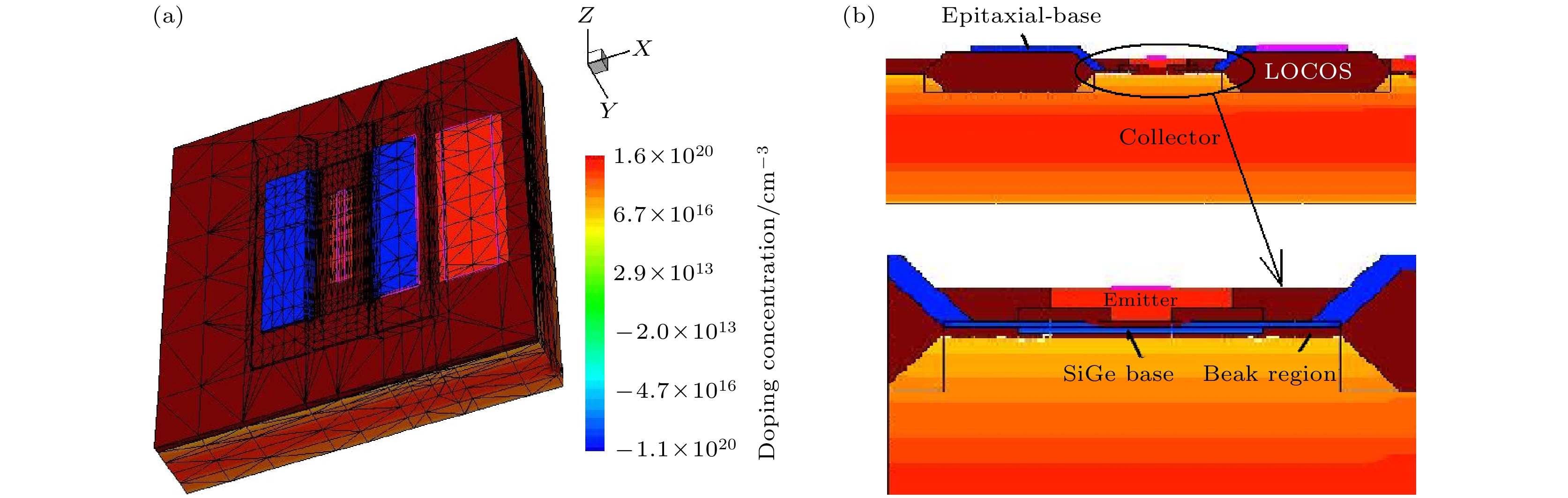
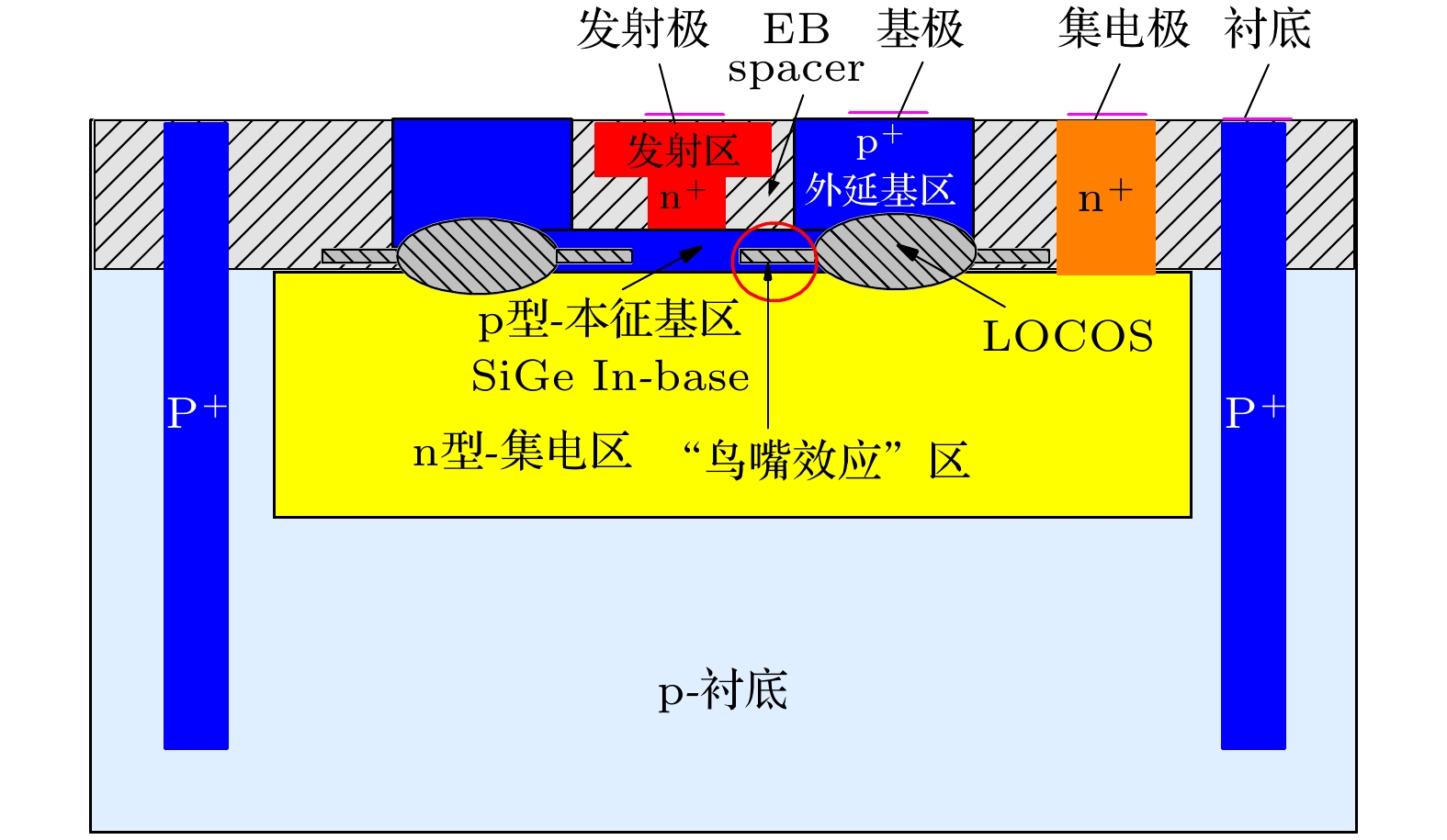
图 2 器件结构仿真模型 (a) 器件三维结构; (b) 内部结构二维剖面图(上)及局部放大视图(下)
Fig. 2. Device model of simulation: (a) Three dimensional (3D) structure; (b) two dimensional (2D) cross section of SiGe HBT.
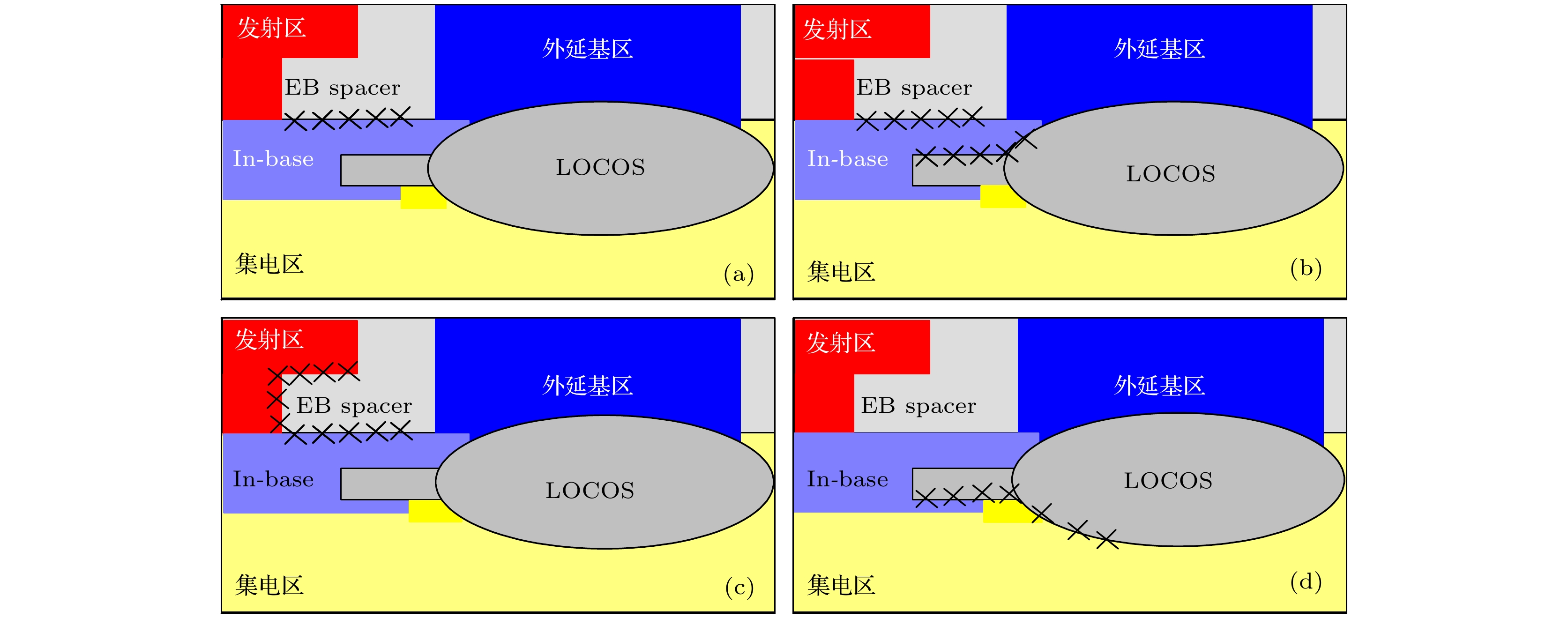
图 3 不同Si/SiO2界面位置处添加traps模型的示意图 (a)本征基区In-base与EB spacer界面添加traps; (b)本征基区In-base与LOCOS上界面添加trap; (c)发射区和EB spacer界面添加traps; (d)本征基区In-base与LOCOS下界面、集电区与LOCOS下界面添加traps
Fig. 3. Traps on different location of Si/SiO2 interface: (a) Traps on interface between In-base and EB spacer; (b) traps on interface between In-base and upside LOCOS; (c) traps on interface between emitter and EB spacer; (d) traps on interface between below side LOCOS and In-base, up side and collector .

图 4 添加traps模型前后SiGe HBT Gummel特性变化 (a)正向Gummel; (b)反向Gummel
Fig. 4. Gummel characteristics of SiGe HBT in the pre and post traps: (a) Forward Gummel characteristics; (b) reverse Gummel characteristics.

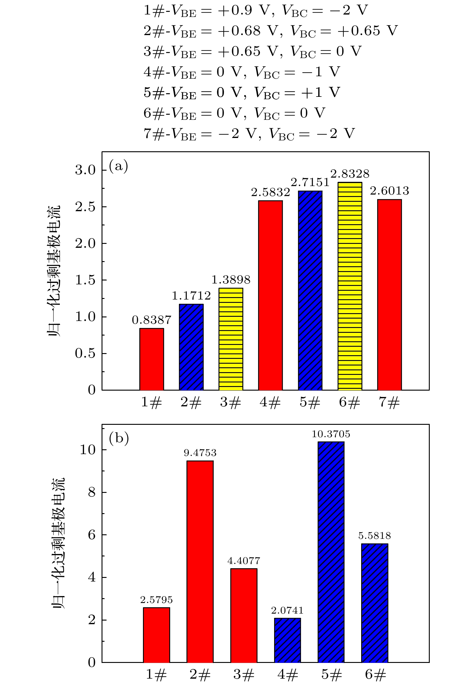
图 5 对比只在器件一处Si/SiO2界面添加traps模型的正向Gummel特性变化 (a)正向Gummel基极电流变化; (b)正向Gummel特性归一化过剩基极电流
Fig. 5. Forward Gummel characteristic with the traps model added toonly one Si/SiO2 interface: (a) Base current of forward Gummel; (b) normalized excess base current of forward Gummel.
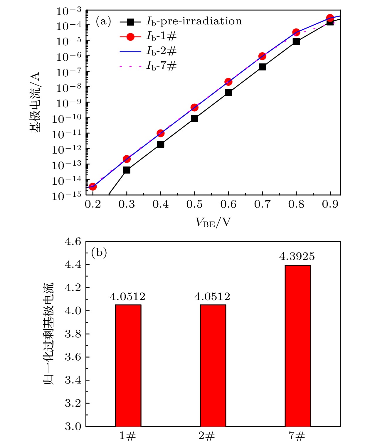
图 6 对比本征基区与EB spacer界面添加traps模型的正向Gummel特性变化 (a) 正向Gummel基极电流变化; (b) 正向Gummel特性归一化过剩基极电流
Fig. 6. Forward Gummel characteristic with the traps model added to theinterface of intrinsic base and EB spacer: (a) Base current of forward Gummel; (b) normalized excess base current.
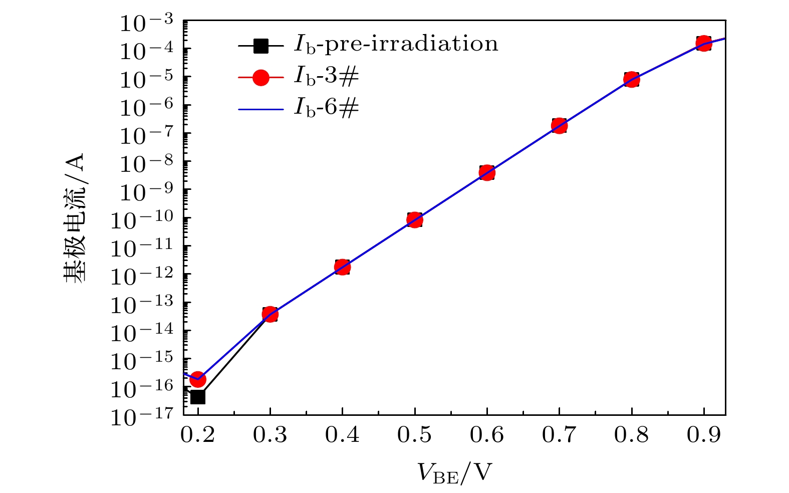
图 7 对比LOCOS隔离下界面添加traps模型的正向Gummel特性基极电流变化
Fig. 7. Base current of forward Gummel characteristic with the traps model added to theinterface on the below side of LOCOS.
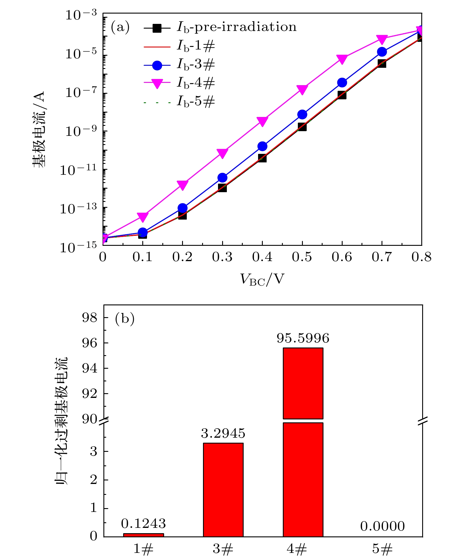
图 8 对比只在器件一处Si/SiO2界面添加traps模型的反向Gummel特性变化 (a)反向Gummel基极电流变化; (b)反向Gummel特性归一化过剩基极电流
Fig. 8. Reverse Gummel characteristic with the traps model added only to one Si/SiO2 interface: (a) Base current of reverse Gummel; (b) normalized excess base current of reverse Gummel.
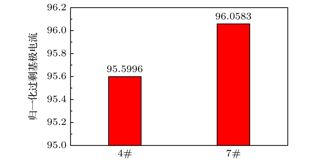
图 9 对比本征基区与LOCOS隔离上界面分布陷阱缺陷的归一化过剩基极电流
Fig. 9. Normalized excess base current of reverse Gummel with the traps model added to the interface of intrinsic base and upside LOCOS.

图 10 对比本征基区与LOCOS隔离下界面分布陷阱缺陷的归一化过剩基极电流
Fig. 10. Normalized excess base current of reverse Gummel with the traps model added to the interface of intrinsic base and below LOCOS.
-
[1] Datta K, Hashemi H, Performance L 2014 IEEE J. Solid-State Circuits 49 2150
Google Scholar
[2] 张晋新, 郭红霞, 郭旗, 文林, 崔江维, 席善斌, 王信, 邓伟 2013 物理学报 62 048501
Google Scholar
Zhang J X, Guo H X, Guo Q, Wen L, Cui J W, Xi S B, Wang X, Deng W 2013 Acta Phys. Sin. 62 048501
Google Scholar
[3] Cressler J D 2004 Silicon-Germanium Heterojunction Bipolar Transistor (Boston: John Wiley & Sons, Ltd) p23
[4] Garcia E R, ZerounianN, CrozatP, Aguilar M E, Chevalier P, ChantreA, Aniel F 2009 Cryogenics 49 620
Google Scholar
[5] 张晋新, 贺朝会, 郭红霞, 唐杜, 熊涔, 李培, 王信 2014 物理学报 63 248503
Google Scholar
Zhang J X, He C H, Guo H X, Tang D, Xiong C, Li P, Wang X 2014 Acta Phys. Sin. 63 248503
Google Scholar
[6] Pratapgarhwala M 2005 Ph. D. Dissertation (Atlanta: Georgia Institute of Technology)
[7] Bellini M 2009 Ph. D. Dissertation (Atlanta: Georgia Institute of Technology)
[8] Ullan M, Wilder M, Spieler H, Spencer E, Rescia S, Newcomer F M, Martinez-McKinney F, Kononenko W, Grillo A A, Diez S 2012 Nucl. Instrum. Method Phys. Res. B 724 41
[9] Praveen K C, Pushpa N, Naik P S, Cressler J D, Tripathi A, Gnana A P 2012 Nucl. Instrum. Method Phys. Res. B 273 43
Google Scholar
[10] Sun Y B, Fu J, Xu J, Wang Y D, Zhou W, Zhang W, Cui J, Li G Q, Liu Z H 2013 Nucl. Instrum. Method Phys. Res. B 312 77
Google Scholar
[11] Díez S, Lozano M, Pellegrini G, Campabadal F, Mandic I, Knoll D, Heinemann B, Ullánet M 2009 IEEE Trans. Nucl. Sci. 56 1931
Google Scholar
[12] Fleetwood Z E, Cardoso A S, Song I, Wilcox E, Lourenco N E, Philips S D, Arora R, Amouzou P P, Cressler J D 2014 IEEE Trans. Nucl. Sci. 61 2915
Google Scholar
[13] Yan G, Bi J, Xu G, Xi K, Li B, Fan L, Yin H 2020 IEEE Access 8 154898
Google Scholar
[14] 曹杨, 习凯, 徐彦楠, 李梅, 李博, 毕津顺, 刘明 2019 物理学报 68 038501
Google Scholar
Cao Y, Xi K, Xu Y, Li M, Li B, Bi J, Liu M 2019 Acta Phys. Sin. 68 038501
Google Scholar
[15] Banerje G, Niu G, Cressler J D, Clark S D, Palmer M J, Ahlgren D C 1999 IEEE Trans. Nucl. Sci. 46 1620
Google Scholar
[16] Fleetwood D M 2013 IEEE Trans. Nucl. Sci. 60 1706
Google Scholar
[17] Sutton A K, Prakash A P G, Jun B, Zhao E, Bellini M, Pellish J, Diestelhorst R M, Carts M A, Phan A, Ladbury R, Cressler J D, Fleetwood D M 2006 IEEE Trans. Nucl. Sci. 53 3166
Google Scholar
[18] Xu Y, Bi J, Xu G, Xi K, Li B, Wang H, Liu M 2018 Chin. Phys. Lett. 35 118501
Google Scholar
[19] Boch J, Saigne F, Touboul A D, Ducret S, Carlotti J F, Bernard M, Schrimpf R D, Wrobel F, Sarrabayrouse G 2006 Appl. Phys. Lett. 88 232113
Google Scholar
[20] Zhang J X, Guo Q, Guo H X, Lu W, He C H, Wang X, Li P, Liu M H 2016 IEEE Trans. Nucl. Sci. 63 1251
Google Scholar
[21] Zhang J X, Guo Q, Guo H X, Lu W, He C H, Wang X, Li P, Wen L 2018 Microelectron. Reliab. 84 105
Google Scholar
[22] Zhang S, Cressler J D, Niu G F, Marshall C J, Marshall P W, Kim H S, Reed R A, Palmer M J, Joseph A J, Harame D L 2003 Solid-State Electron. 47 1729
Google Scholar

 下载:
下载:
计量
- 文章访问数: 8395
- PDF下载量: 100
- 被引次数: 0
