


-
阻变存储器由于具有读取速度快、存储密度大、存储时间长、低功耗和结构简单等主要特点, 已被看为下一代非易失性随机存储器的重要候选者. 本文研究了Ni/ZnO/BiFeO3/ZnO/ITO多层纳米薄膜器件的电阻开关特性, 发现器件具有明显的双极性电阻开关效应, 而且样品的电阻开关特性随外加磁场的干涉会有明显变化, 包括开关比、耐受性和电导率. 磁场对Ni/ZnO/BiFeO3/ZnO/ITO薄膜器件的显著调控作用应该起源于磁场使得Ni/ZnO界面处的肖特基势垒改变. 这项工作可以为磁控电阻开关效应提供一种可能的新机制, 在未来的存储器器件中具有重要的潜在应用价值.The 21st century is an era of information. In recent years, people’s demand for better data storage performance and stronger data processing capacity of memorizer has been increasing, which has prompted continuous improvement and innovation of semiconductor integrated processes and technologies and accelerated the research progress of the next generation of memory devices to break through the limits of Moore’s law. Resistive memory has been regarded as an important candidate for the next generation of non-volatile random access memory due to its main characteristics such as fast reading speed, high storage density, long storage time, low power consumption, and simple structure. Resistive switching effects have been observed in various transition metal oxides and complex perovskite oxides, but the appropriate description of the resistive switching drive mechanism is still an important issue in the development of resistive random access memories. Therefore, further research is very important to clearly explain the phenomenon of resistance switching. With the demand for data storage and sensor applications increasing, materials with excellent ferroelectric and ferromagnetic properties have attracted great attention. The ZnO is an important semiconductor material with excellent optical and electrical properties. Bismuth ferrate (BiFeO3) has received much attention due to its excellent properties in epitaxial and polycrystalline thin films, with hundreds of publications devoted to it in the past few years. The ZnO and BiFeO3 are both important electronic materials and have important application value. Therefore, ZnO/BiFeO3/ZnO structure is adopted in this work to study the resistance switch characteristics. The resistance conversion effect in ZnO/BiFeO3/ZnO structure is measured. In this work, the Ni/ZnO/BiFeO3/ZnO/ITO multilayer nano-film storage device is prepared by magnetron sputtering coating technology. The device is characterized by X-ray diffractometer, scanning electron microscope and other equipment, and its resistance performance is further tested by Keithley 2400. The device exhibits obvious bipolar resistance switching effect, and the resistance switching characteristics of the sample, including switching ratio, tolerance and conductivity, vary significantly with the interference of the applied magnetic field. The bipolar resistance switching effect can be explained by the capture and release of oxygen vacancies trapped inside the material. The effect of magnetic field on Ni/ZnO/BiFeO3/ZnO/ITO thin film device should be attributed to the change of schottky barrier at Ni/ZnO interface, caused by magnetic field.
-
Keywords:
- multilayer nanofilm structure /
- resistance switching effect /
- magnetic control /
- oxygen vacancies
[1] Zhou G D, Sun B, Hu X, Sun L, Zou Z, Xiao B, Qiu W, Wu B, Li J, Han J, Liao L, Xu C, Xiao G, Xiao L, Cheng J, Zheng S, Wang L, Song Q, Duan S 2021 Adv. Sci. 7 2003765
 Google Scholar
[2] Ren S Q, Qin H W, Bu J P, Zhu G C, Xie J H, Hu J F 2015 Appl. Phys. Lett. 107 062404
Google Scholar
[3] 庞华, 邓宁 2014 物理学报 63 147301
Google Scholar
Pang H, Deng N 2014 Acta Phys. Sin. 63 147301
Google Scholar
[4] Wang J S, Liang D D, Wu L C, Li X P, Chen P 2018 Solid State Commun. 275 8
Google Scholar
[5] Sun B, Zhou G D, Guo T, Zhou Y N, Wu Y A 2020 Nano Energy 75 104938
Google Scholar
[6] Li H W, Wu S X, Hu P, Li D, Wang G L, Li S W 2017 Phys. Lett. A 381 2127
Google Scholar
[7] 何朝滔, 卢羽, 李秀林, 陈鹏 2022 物理学报 71 086102
Google Scholar
He C T, Lu Y, Li X L, Chen P 2022 Acta Phys. Sin. 71 086102
Google Scholar
[8] Wang Q W, Zhu Y D, Liu X L, Zhao M, Wei M C, Zhang F, Zhang Y, Sun B L, Li M Y 2015 Appl. Phys. Lett. 107 063502
Google Scholar
[9] Chen G, Song C, Chen C, Gao S, Zeng F, Pan F 2012 Adv. Mater. 24 3515
Google Scholar
[10] Selim F, Weber M, Solodovnikov D, Lynn K 2007 Phys. Rev. Lett. 99 085502
Google Scholar
[11] Xiong C Y, Lu Z Y, Yin S Q, Mou H M, Zhang X Z 2019 AIP Adv. 9 105030
Google Scholar
[12] Wang J M, Zhang X Z, Piao H G, Luo Z C, Xiong C Y, Wang X F, Yang F H 2014 Appl. Phys. Lett. 104 243511
Google Scholar
[13] Zhou G D, Wang Z R, Sun B, Zhou F C, Sun L F, Zhao H B, Hu X F, Peng X Y, Yan J, Wang H M, Wang W H, Li J, Yan B T, Kuang D L , Wang Y C, Wang L D, Duan S K 2022 Adv. Electron. Mater. 8 2101127
Google Scholar
[14] Tang Y Y, Zhang X W, Lu Y, Li X L, Chen P 2021 Funct. Mater. Lett. 14 2150025
Google Scholar
[15] Chang W Y, Lai Y C, Wu T B, Wang S F, Chen F, Tsai M J 2008 Appl. Phys. Lett. 92 022110
Google Scholar
[16] Hsieh W K, Lam K T, Chang S J 2015 Mater. Sci. Semicond. Process. 35 30
Google Scholar
[17] Ren S X, Sun G W, Zhao J, Dong J Y, Wei Y, Ma Z C, Zhao X, Chen W 2014 Appl. Phys. Lett. 104 232406
Google Scholar
[18] Ren S X, Dong W C, Tang H, Tang L Z, Li Z H, Sun Q, Yang H F, Yang Z G, Zhao J J 2019 Appl. Surf. Sci. 488 92
Google Scholar
[19] Zheng P P, Sun B, Chen Y Z, Elshekh H, Yu T, Mao S S, Zhu S H, Wang H Y, Zhao Y, Yu Z 2019 Appl. Mater. Today 14 21
Google Scholar
[20] Liang D D, Li X P, Wang J S, Wu L C, Chen P 2018 Solid State Electron. 145 46
Google Scholar
[21] Wang T, Cheng L L, Wang C X, Cheng W M, Wang H W, Sun H J, Chen J C, Miao X S 2020 IEEE Trans. Magn. 56 7505004
Google Scholar
[22] Sun B, Liu Y H, Zhao W X, Chen P 2015 RSC Adv. 5 13513
Google Scholar
[23] Zheng W C, Wang Y C, Jin C, Yin R H, Li D, Wang P, Liu S S, Wang X Y, Zheng D X, Bai H L 2020 Phys. Chem. Chem. Phys. 22 13277
Google Scholar
[24] Jena A K, Ajit K S, Mohanty J. 2020 Appl. Phys. Lett. 116 092901
Google Scholar
[25] Dwipak P S, Narayana J S 2017 Sci. Rep. 7 17224
Google Scholar
[26] Karuppasamy K, Rabani I, Vikraman D, Bathula C, Theerthagiri J, Bose R, Yim C J, Kathalingam A, Seo Y S, Kim H S 2021 Environ. Pollut. 272 116018
Google Scholar
[27] Xu J, Chang Y G, Zhang Y Y, Ma S Y, Qu Y, Xu C T 2008 Appl. Surf. Sci. 255 1996
Google Scholar
[28] Zhong T T, Qin Y F, Lv F Z, Qin H J, Tian X D 2021 Nanoscale Res. Lett. 16 178
Google Scholar
[29] Li X L, Li X P, Chen P 2021 J. Electron. Mater. 50 3972
Google Scholar
[30] Kim B, Mahata C, Ryu H, Ismail M, Yang B, Kim S 2021 Coatings 11 451
Google Scholar
[31] Hu C, Wang Q, Bai S, Xu M, He D Y, Lu D Y, Qi J 2017 Appl. Phys. Lett. 110 073501
Google Scholar
[32] Gu T K 2014 J. Appl. Phys. 115 203707
Google Scholar
[33] Junga K, Kimb K, Songc S, Park K 2019 Microelectron. Eng. 216 111015
Google Scholar
[34] 陈勇 2015 硕士学位论文 (开封: 河南大学)
Chen Y 2015 M. S. Thesis (Kaifeng: Henan University) (in Chinese)
-
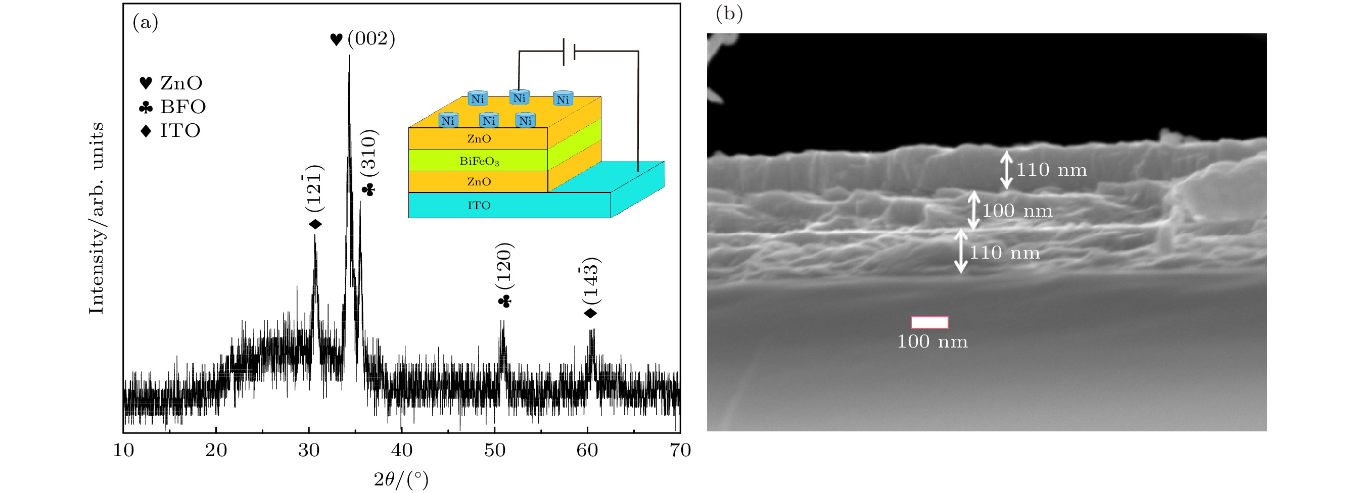
图 1 (a) ZnO/BiFeO3/ZnO/ITO器件的XRD谱图, 插图为其结构示意图; (b) ZnO/BiFeO3/ZnO结构的SEM图像
Fig. 1. (a) XRD pattern of ZnO/BiFeO3/ZnO/ITO device (the inset shows the structure of the sample); (b) SEM image of ZnO/BiFeO3/ZnO.
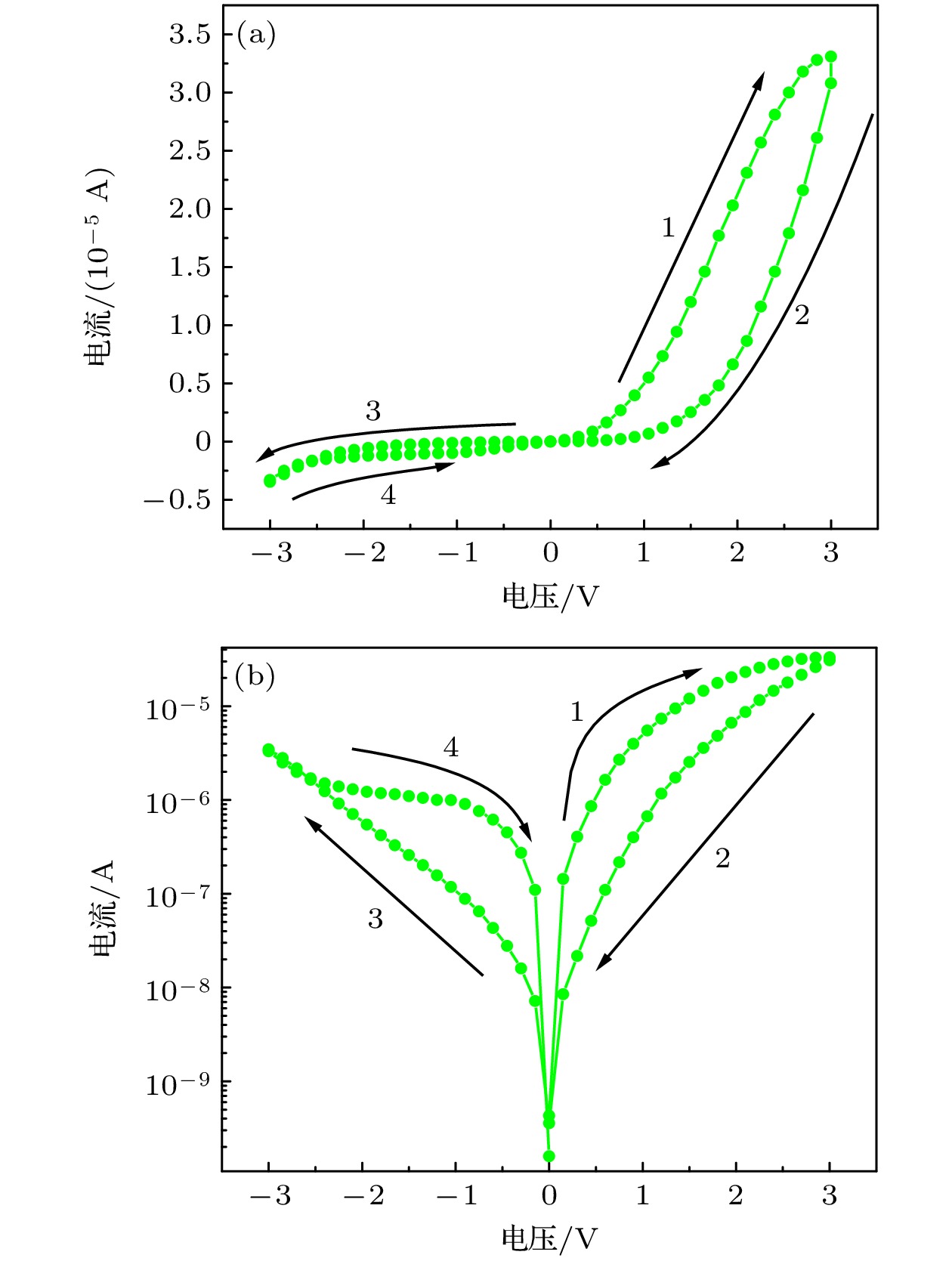
图 2 (a) Ni/ZnO/BiFeO3/ZnO/ITO器件的I-V曲线; (b)相应的对数图
Fig. 2. (a) I-V curve of the Ni/ZnO/BiFeO3/ZnO/ITO device; (b) the corresponding logarithmic graph.
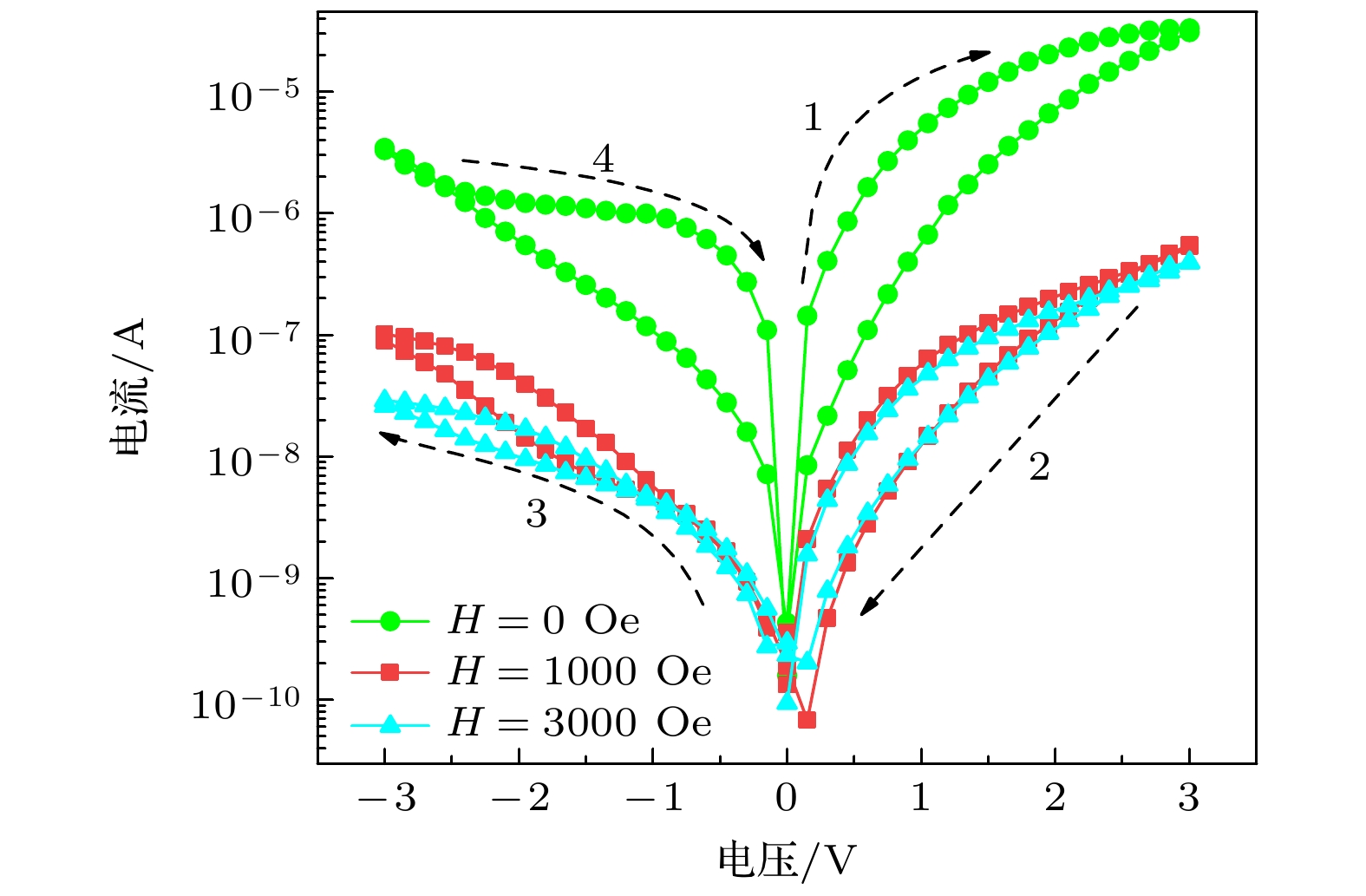
图 3 Ni/ZnO/BiFeO3/ZnO/ITO器件在有磁场和无磁场下的I-V曲线A/m)
Fig. 3. I-V curves of the Ni/ZnO/BiFeO3/ZnO/ITO device with and without magnetic field.
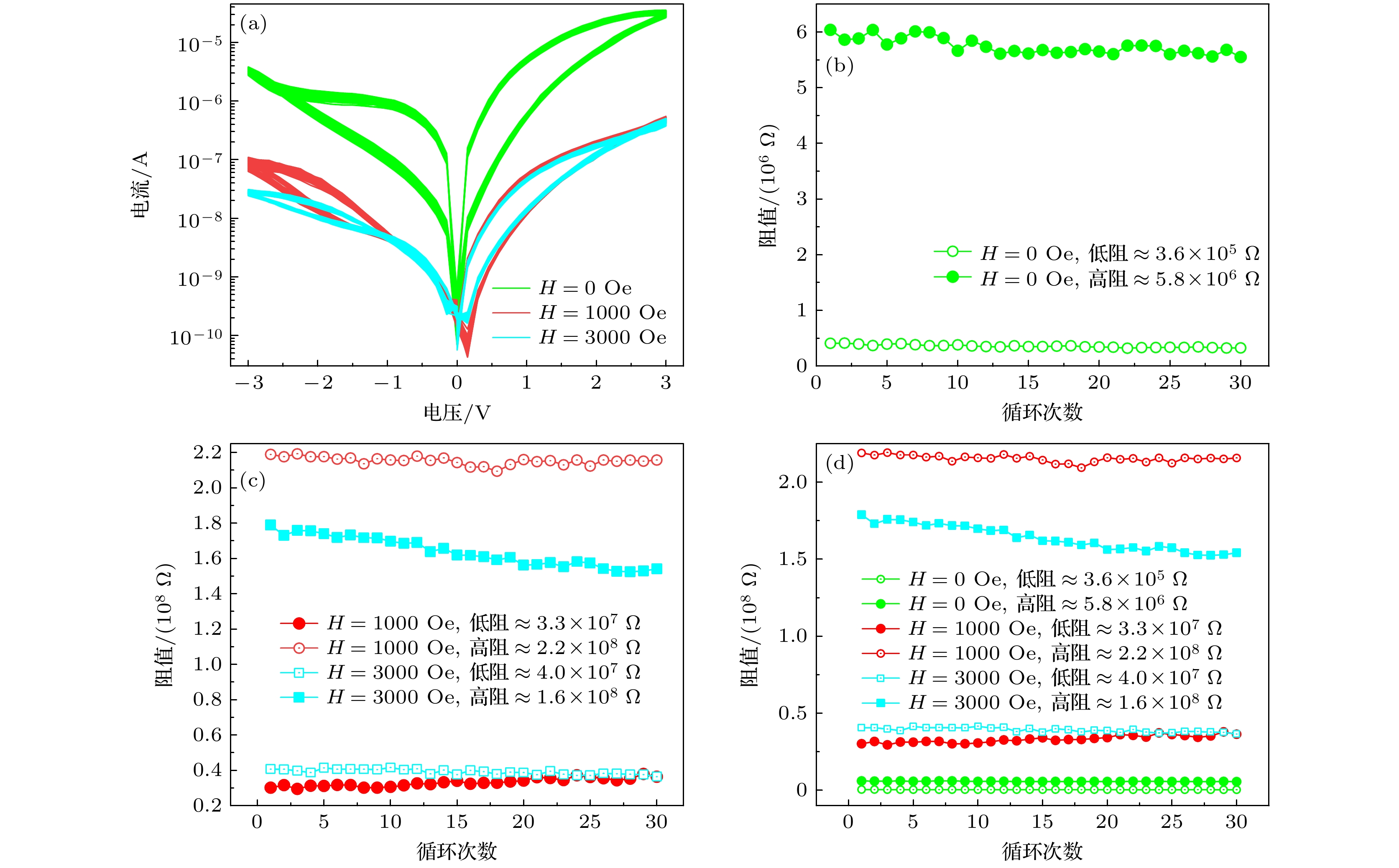
图 4 (a) Ni/ZnO/BiFeO3/ZnO/ITO器件循环30圈的I-V曲线; (b)器件在0.6 V下的高低电阻分布图; (c)器件在外加磁场时0.6 V下的高低电阻分布示意图; (d)为(b)和(c)分布图的组合图
Fig. 4. (a) I-V curves of the Ni/ZnO/BiFeO3/ZnO/ITO device with 30 cycles; (b) high and low resistance distribution diagram of the device at 0.6 V; (c) high and low resistance distribution diagram of the device at 0.6 V with external magnetic field; (d) combination diagram of panels (b) and (c).

图 5 Ti/ZnO/BiFeO3/ZnO/ITO器件加磁与不加磁I-V曲线结合图
Fig. 5. Combination diagram of I-V curves of the Ti/ZnO/BiFeO3/ZnO/ITO device with magnetized and unmagnetized.
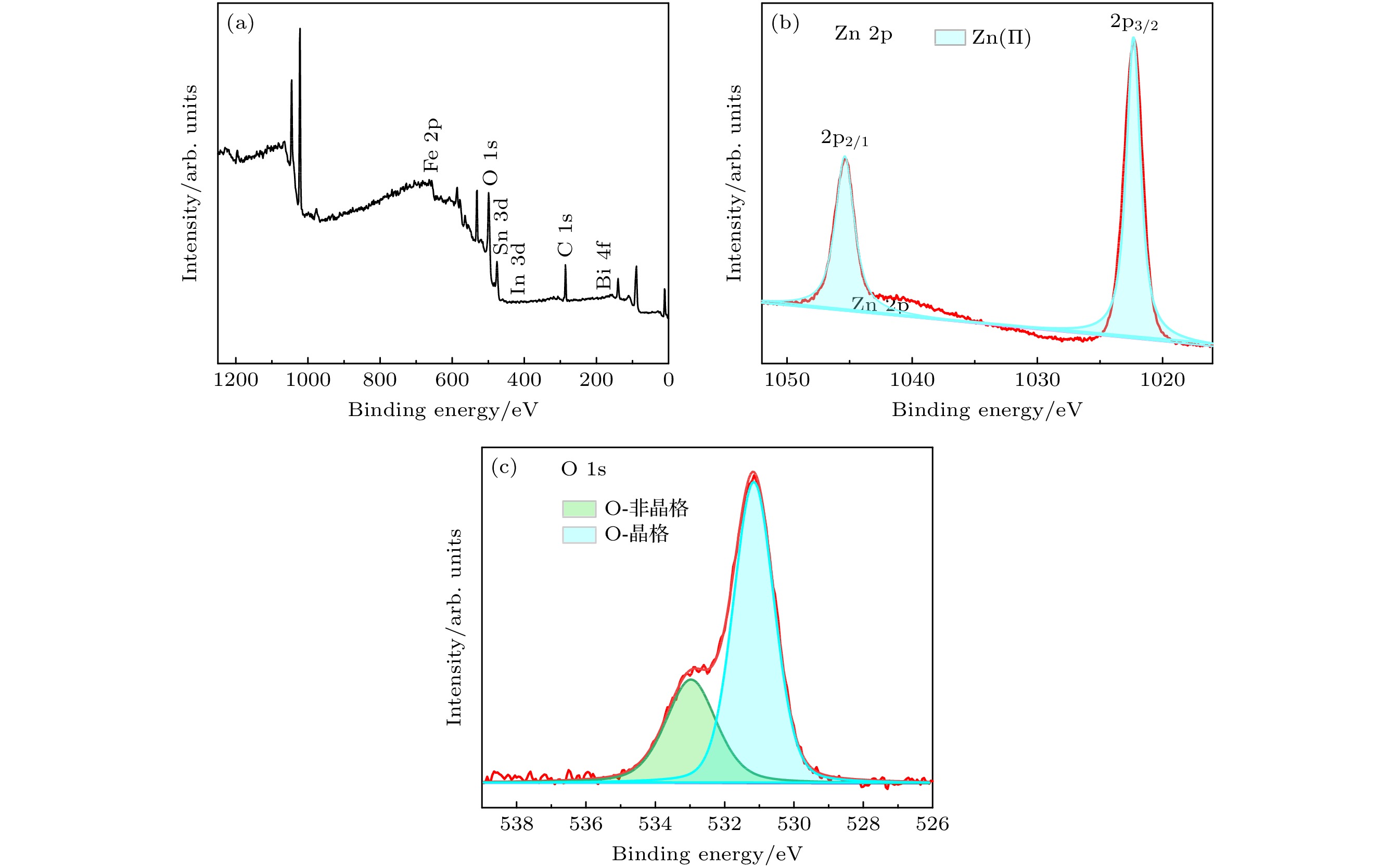
图 6 (a) ZnO/BiFeO3/ZnO/ITO器件的XPS图; (b) Zn 2p的XPS图; (c) O 1s的XPS图
Fig. 6. (a) XPS survey spectrum of ZnO/BiFeO3/ZnO/ITO device; (b) XPS spectra of Zn 2p patterns; (c) XPS spectra of O 1s patterns

图 7 (a) 低阻态下的双对数拟合图; (b)高阻态下的lnI与
$ \sqrt{V} $ 拟合图; (c)外加磁场时低阻态下的双对数拟合图; (d)外加磁场时高阻态下的lnI与$ \sqrt{V} $ 拟合图Fig. 7. (a) The log-log fitting diagram at LRS state; (b) lnI-
$ \sqrt{V} $ fitting diagram at HRS state; (c) log-log fitting diagram at LRS state with external magnetic field; (d) lnI-$ \sqrt{V} $ fitting diagram at HRS state with external magnetic field. -
[1] Zhou G D, Sun B, Hu X, Sun L, Zou Z, Xiao B, Qiu W, Wu B, Li J, Han J, Liao L, Xu C, Xiao G, Xiao L, Cheng J, Zheng S, Wang L, Song Q, Duan S 2021 Adv. Sci. 7 2003765
Google Scholar
[2] Ren S Q, Qin H W, Bu J P, Zhu G C, Xie J H, Hu J F 2015 Appl. Phys. Lett. 107 062404
Google Scholar
[3] 庞华, 邓宁 2014 物理学报 63 147301
Google Scholar
Pang H, Deng N 2014 Acta Phys. Sin. 63 147301
Google Scholar
[4] Wang J S, Liang D D, Wu L C, Li X P, Chen P 2018 Solid State Commun. 275 8
Google Scholar
[5] Sun B, Zhou G D, Guo T, Zhou Y N, Wu Y A 2020 Nano Energy 75 104938
Google Scholar
[6] Li H W, Wu S X, Hu P, Li D, Wang G L, Li S W 2017 Phys. Lett. A 381 2127
Google Scholar
[7] 何朝滔, 卢羽, 李秀林, 陈鹏 2022 物理学报 71 086102
Google Scholar
He C T, Lu Y, Li X L, Chen P 2022 Acta Phys. Sin. 71 086102
Google Scholar
[8] Wang Q W, Zhu Y D, Liu X L, Zhao M, Wei M C, Zhang F, Zhang Y, Sun B L, Li M Y 2015 Appl. Phys. Lett. 107 063502
Google Scholar
[9] Chen G, Song C, Chen C, Gao S, Zeng F, Pan F 2012 Adv. Mater. 24 3515
Google Scholar
[10] Selim F, Weber M, Solodovnikov D, Lynn K 2007 Phys. Rev. Lett. 99 085502
Google Scholar
[11] Xiong C Y, Lu Z Y, Yin S Q, Mou H M, Zhang X Z 2019 AIP Adv. 9 105030
Google Scholar
[12] Wang J M, Zhang X Z, Piao H G, Luo Z C, Xiong C Y, Wang X F, Yang F H 2014 Appl. Phys. Lett. 104 243511
Google Scholar
[13] Zhou G D, Wang Z R, Sun B, Zhou F C, Sun L F, Zhao H B, Hu X F, Peng X Y, Yan J, Wang H M, Wang W H, Li J, Yan B T, Kuang D L , Wang Y C, Wang L D, Duan S K 2022 Adv. Electron. Mater. 8 2101127
Google Scholar
[14] Tang Y Y, Zhang X W, Lu Y, Li X L, Chen P 2021 Funct. Mater. Lett. 14 2150025
Google Scholar
[15] Chang W Y, Lai Y C, Wu T B, Wang S F, Chen F, Tsai M J 2008 Appl. Phys. Lett. 92 022110
Google Scholar
[16] Hsieh W K, Lam K T, Chang S J 2015 Mater. Sci. Semicond. Process. 35 30
Google Scholar
[17] Ren S X, Sun G W, Zhao J, Dong J Y, Wei Y, Ma Z C, Zhao X, Chen W 2014 Appl. Phys. Lett. 104 232406
Google Scholar
[18] Ren S X, Dong W C, Tang H, Tang L Z, Li Z H, Sun Q, Yang H F, Yang Z G, Zhao J J 2019 Appl. Surf. Sci. 488 92
Google Scholar
[19] Zheng P P, Sun B, Chen Y Z, Elshekh H, Yu T, Mao S S, Zhu S H, Wang H Y, Zhao Y, Yu Z 2019 Appl. Mater. Today 14 21
Google Scholar
[20] Liang D D, Li X P, Wang J S, Wu L C, Chen P 2018 Solid State Electron. 145 46
Google Scholar
[21] Wang T, Cheng L L, Wang C X, Cheng W M, Wang H W, Sun H J, Chen J C, Miao X S 2020 IEEE Trans. Magn. 56 7505004
Google Scholar
[22] Sun B, Liu Y H, Zhao W X, Chen P 2015 RSC Adv. 5 13513
Google Scholar
[23] Zheng W C, Wang Y C, Jin C, Yin R H, Li D, Wang P, Liu S S, Wang X Y, Zheng D X, Bai H L 2020 Phys. Chem. Chem. Phys. 22 13277
Google Scholar
[24] Jena A K, Ajit K S, Mohanty J. 2020 Appl. Phys. Lett. 116 092901
Google Scholar
[25] Dwipak P S, Narayana J S 2017 Sci. Rep. 7 17224
Google Scholar
[26] Karuppasamy K, Rabani I, Vikraman D, Bathula C, Theerthagiri J, Bose R, Yim C J, Kathalingam A, Seo Y S, Kim H S 2021 Environ. Pollut. 272 116018
Google Scholar
[27] Xu J, Chang Y G, Zhang Y Y, Ma S Y, Qu Y, Xu C T 2008 Appl. Surf. Sci. 255 1996
Google Scholar
[28] Zhong T T, Qin Y F, Lv F Z, Qin H J, Tian X D 2021 Nanoscale Res. Lett. 16 178
Google Scholar
[29] Li X L, Li X P, Chen P 2021 J. Electron. Mater. 50 3972
Google Scholar
[30] Kim B, Mahata C, Ryu H, Ismail M, Yang B, Kim S 2021 Coatings 11 451
Google Scholar
[31] Hu C, Wang Q, Bai S, Xu M, He D Y, Lu D Y, Qi J 2017 Appl. Phys. Lett. 110 073501
Google Scholar
[32] Gu T K 2014 J. Appl. Phys. 115 203707
Google Scholar
[33] Junga K, Kimb K, Songc S, Park K 2019 Microelectron. Eng. 216 111015
Google Scholar
[34] 陈勇 2015 硕士学位论文 (开封: 河南大学)
Chen Y 2015 M. S. Thesis (Kaifeng: Henan University) (in Chinese)

 下载:
下载:


计量
- 文章访问数: 6615
- PDF下载量: 94
- 被引次数: 0
