


-
本文针对N型和P型碳纳米管场效应晶体管(carbon nanotube field-effect transistor, CNTFET)开展了10 keV-X射线的总剂量效应研究. 结果表明, 不同类型的晶体管在辐照后均出现阈值电压漂移、跨导下降、亚阈值摆幅上升和饱和电流下降的现象; 辐照过程中, 施加浮空偏置的N型器件较开态偏置损伤更严重, 而施加开态偏置的P型器件较浮空偏置损伤更严重; N型器件辐照后回滞宽度减小且随着沟道尺寸的增大总剂量损伤愈发严重. 辐照过程中产生的陷阱电荷是造成器件参数退化的主要原因; 不同类型器件在辐照过程中施加的栅极偏置会影响栅极介质层中陷阱对电子或空穴的捕获, 从而使器件呈现不同的辐射损伤特征; 辐照后N型器件回滞宽度减小可能是因为辐照产生的带负电陷阱电荷阻碍了水分子、OH基团和栅极介质层中陷阱对电子的捕获; 此外, 晶体管的沟道尺寸也会影响辐射响应, 尺寸越大, 辐照过程中栅极介质层中和界面处产生陷阱电荷越多, 导致晶体管损伤更为严重.
-
关键词:
- 碳纳米管场效应晶体管 /
- X射线辐照 /
- 总剂量效应
To further understand the patterns and mechanisms of total ionizing dose (TID) radiation damage in carbon nanotube field-effect transistor (CNTFET), the total dose effects of 10 keV X-ray irradiation on N-type and P-type CNTFETs are investigated in this work. The irradiation dose rate is 200 rad(Si)/s, with a cumulative dose of 100 krad(Si) for N-type devices and 90 krad(Si) for P-type devices. The differences in TID effect between N-type and P-type CNTFETs under the conditions of floating gate bias and on-state bias, the influence of irradiation on the hysteresis characteristics of N-type CNTFETs, and the influence of channel sizes on the TID effects of N-type CNTFETs are also explored. The results indicate that both types of transistors, after being irradiated, exhibit the threshold voltage shift, transconductance degradation, increase in subthreshold swing, and decrease in saturation current. In the irradiation process, N-type devices under floating gate bias suffer more severe damage than those under on-state bias, while P-type devices under on-state bias experience more significant damage than those under floating gate bias. The hysteresis widths of N-type devices decrease after being irradiated, and the TID damage becomes more severe with the increase of channel dimensions. The main reason for the degradation of device parameters is the trap charges generated in the irradiated process. The gate bias applied during irradiation affects the capture of electrons or holes by traps in the gate dielectric, resulting in different radiation damage characteristics for different types of devices. The reduction in the hysteresis width of N-type devices after being irradiated may be attributed to the negatively charged trap charges generated during irradiation, which hinders the capture of electrons by water molecules, OH groups, and traps in the gate dielectric. Moreover, the channel dimensions of the transistors also influence their radiation response: larger channel dimensions result in more trap charges generated in the gate dielectric and at the interface during irradiation, leading to more severe transistor damage.[1] Qiu C G, Zhang Z Y, Xiao M M, Yang Y J, Zhong D L, Peng L M 2017 Science 355 271
 Google Scholar
[2] Franklin A D, Luisier M, Han S J, Tulevski G, Breslin C M, Gignac L, Lundstrom M S, Haensch W 2012 Nano Lett. 12 758
Google Scholar
[3] Chen B Y, Zhang P P, Ding L, Han J, Qiu S, Li Q W, Zhang Z Y, Peng L M 2016 Nano Lett. 16 5120
Google Scholar
[4] Zhu M G, Si J, Zhang Z Y, Peng L M 2018 Adv. Mater. 30 1707068
Google Scholar
[5] Yang Y Y, Ding L, Chen H J, Han J, Zhang Z Y, Peng L M 2018 Nano Res. 11 300
Google Scholar
[6] Shulaker M M, Hills G, Patil N, Wei H, Chen H Y, Wong H S, Mitra S 2013 Nature 501 526
Google Scholar
[7] De Volder M F, Tawfick S H, Baughman R H, Hart A J 2013 Science 339 535
Google Scholar
[8] 刘一凡, 张志勇 2022 物理学报 71 068503
Google Scholar
Liu Y F, Zhang Z Y 2022 Acta Phys. Sin. 71 068503
Google Scholar
[9] 马武英, 陆妩, 郭旗, 何承发, 吴雪, 王信, 丛忠超, 汪波, 玛丽娅 2014 物理学报 63 026101
Google Scholar
Ma W Y, Lu W, Guo Q, He C F, Wu X, Wang X, Cong Z C, Wang B, Maria 2014 Acta Phys. Sin. 63 026101
Google Scholar
[10] 董世剑, 郭红霞, 马武英, 吕玲, 潘霄宇, 雷志锋, 岳少忠, 郝蕊静, 琚安安, 钟向丽, 欧阳晓平 2020 物理学报 69 078501
Google Scholar
Dong S J, Guo H X, Ma W Y, Lv L, Pan X Y, Lei Z F, Yue S Z, Hao R J, Ju A A, Zhong X L, Ouyang X P 2020 Acta Phys. Sin. 69 078501
Google Scholar
[11] Krasheninnikov A, Nordlund K, Sirviö M, Salonen, E, Keinonen J 2001 Phys. Rev. B 63 245405
Google Scholar
[12] Tolvanen A, Kotakoski J, Krasheninnikov A, Nordlund K 2007 Appl. Phys. Lett. 91 173109
Google Scholar
[13] Krasheninnikov A V, Nordlund K 2010 J. Appl. Phys. 107 071301
Google Scholar
[14] Zhao Y D, Li D Q, Xiao L, Liu J K, Xiao X Y, L G H, Jin Y H, Jiang K L, Wang J P, Fan S S, Li Q Q 2016 Carbon 108 363
Google Scholar
[15] Zhang X R, Zhu H P, Peng S A, Xiong G D, Zhu C Y, Huang X N, Cao S R, Zhang J J, Yan Y P, Yao Y, Zhang D Y, Shi J Y, Wang L, Li B, Jin Z 2021 J. Semicond. 42 112002
Google Scholar
[16] Zhu M G, Zhou J S, Sun P K, Peng L M, Zhang Z Y 2021 ACS Appl. Mater. Interfaces 13 47756
Google Scholar
[17] Kanhaiya P S, Yu A, Netzer R, Kemp W, Doyle D, Shulaker M M 2021 ACS Nano 15 17310
Google Scholar
[18] Petrosjanc K O, Adonin A S, Kharitonov I A, Sicheva M V 1994 Proceedings of 1994 IEEE International Conference on Microelectronic Test Structures Moscow, Russia, March 22–25, 1994 p126
[19] Oldham T R, Mclean F B 2002 IEEE T. Nucl. Sci. 50 483
[20] Galloway K F, Gaitan M, Russell T J 1984 IEEE T. Nucl. Sci. 31 1497
Google Scholar
[21] Lu P, Zhu M G, Zhao P X, Fan C W, Zhu H P, Gao J T, Y C, Han Z S, Li B, Liu J, Zhang Z Y 2023 ACS Appl. Mater. Interfaces 15 10936
Google Scholar
[22] McMorrow J J, Cress C D, Affouda C 2012 ACS Nano 6 5040
Google Scholar
[23] Belyakov V V, Pershenkov V S, Zebrev G I, Sogoyan A V, Chumakov A I, Nikiforov A Y, Skorobogatov P K 2003 Russian Microelectron. 32 25
Google Scholar
[24] Ni H Z, Li M, Li X H, Zhu X W, Liu H H, Xu M 2022 IEEE T. Electron Dev. 69 1069
Google Scholar
[25] Kim W, Javey A, Vermesh O, Wang Q, Li Y M, Dai H J, 2003 Nano Letters 3 193
Google Scholar
[26] Chua L L, Zaumseil J, Chang J F, Ou E C, Ho P K, Sirringhaus H, Friend R H 2005 Nature 434 194
Google Scholar
[27] Lee S, Koo B, Shin J, Lee E, Park H, Kim H 2006 Appl. Phys. Lett. 88 99
[28] Cai X, Gerlach C P, Frisbie C D 2007 J. Phys. Chem. C 111 452
Google Scholar
[29] Ha T J, Kiriya D, Chen K, Javey A 2014 ACS Appl. Mater. Interfaces 6 8441
Google Scholar
[30] Wang Y W, Wang S, Ye H D, Zhang W H, Xiang L 2023 IEEE T. Dev. Mater. Re. 23 571
Google Scholar
-
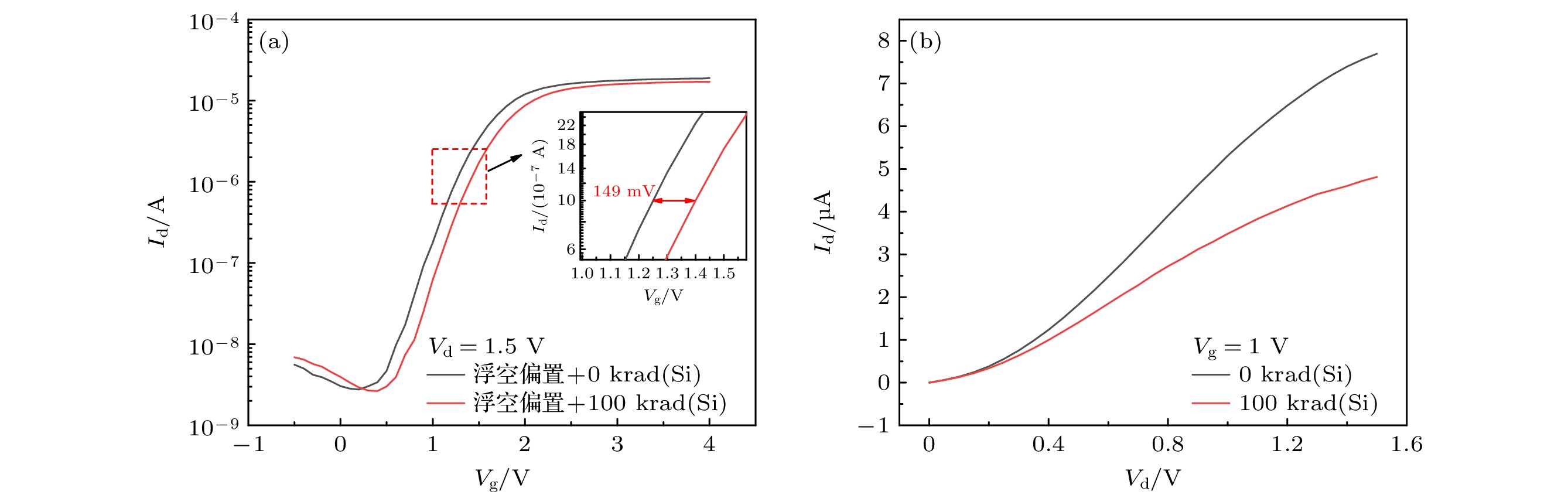
图 2 辐照前后N型器件的电学曲线 (a)转移特性曲线; (b)输出特性曲线
Fig. 2. Electrical curves of N-type devices before and after irradiation: (a) Transfer characteristic curve; (b) output characteristic curve.
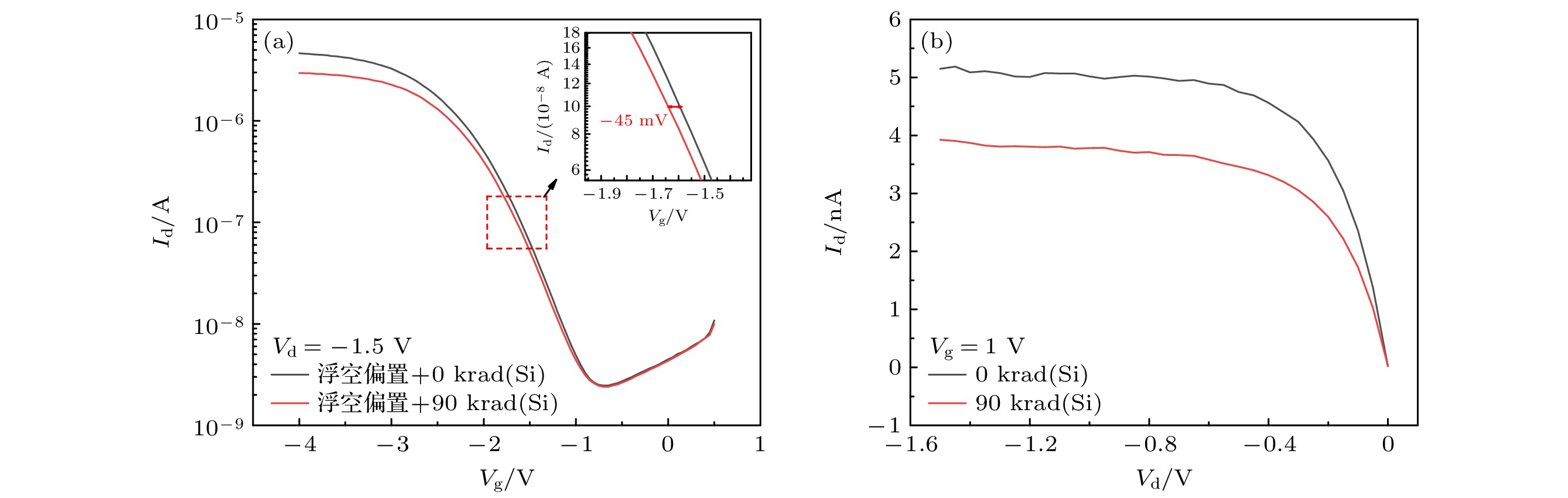
图 3 辐照前后P型器件的电学曲线 (a)转移特性曲线; (b)输出特性曲线
Fig. 3. Electrical curves of P-type devices before and after irradiation: (a) Transfer characteristic curve; (b) output characteristic curve.
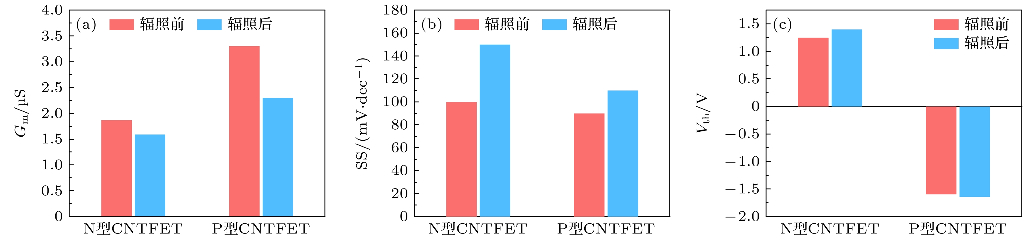
图 4 辐照前后N型和P型器件的电学参数 (a)跨导; (b)亚阈值摆幅; (c)阈值电压
Fig. 4. Electrical parameters of N-type and P-type devices before and after irradiation: (a) Transconductance; (b) subthreshold swing; (c) threshold voltage.

图 5 不同偏置条件下辐照前后的转移特性曲线 (a) N型器件; (b) P型器件
Fig. 5. Transfer characteristic curves before and after irradiation under different bias conditions: (a) N-type devices; (b) P-type devices.
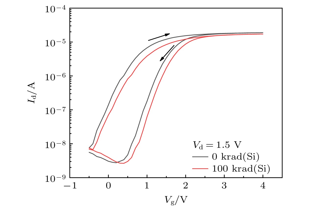
图 6 辐照前后回滞特性的变化
Fig. 6. Changes in hysteresis characteristics before and after irradiation.
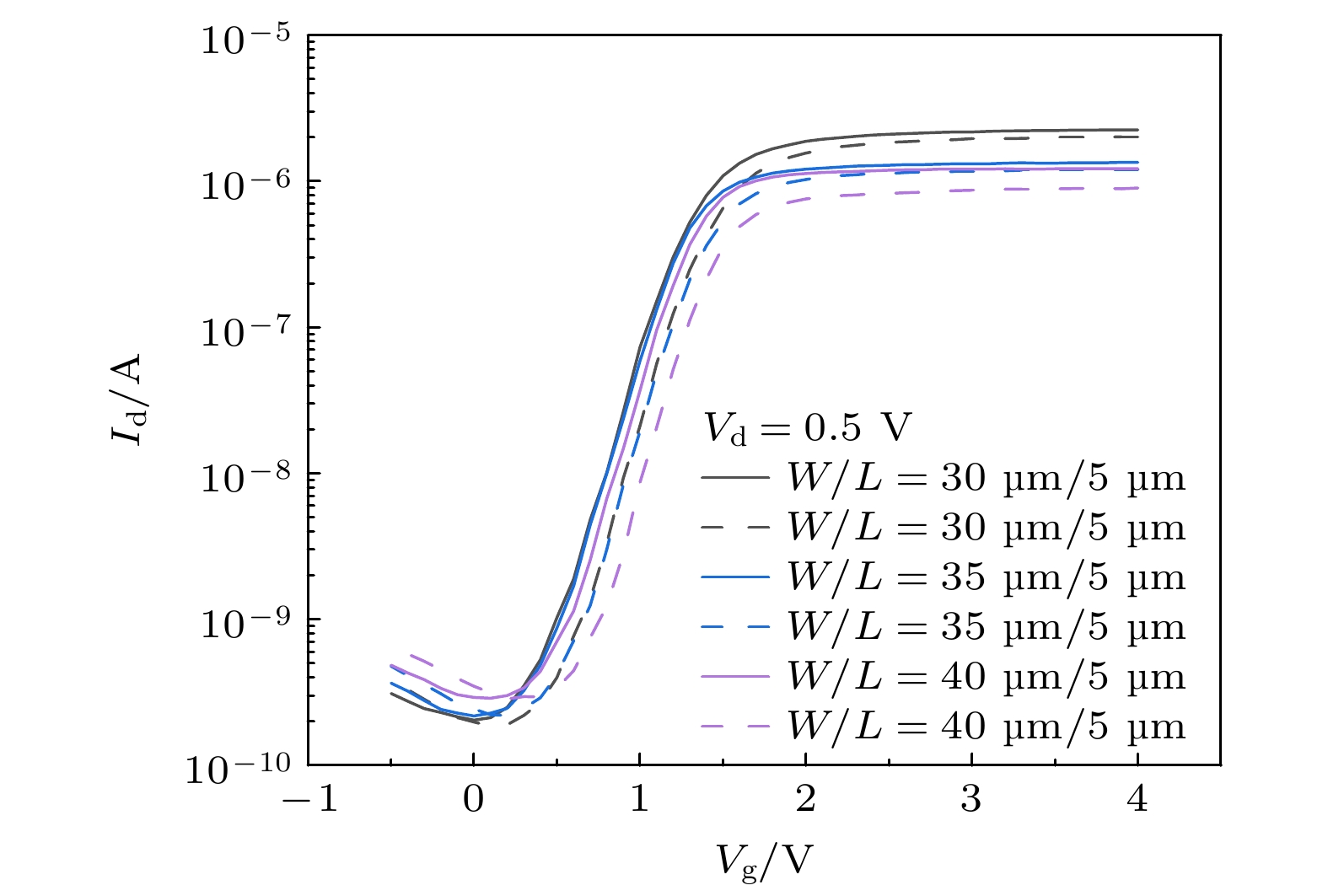
图 7 辐照前后不同沟道尺寸的CNTFET转移曲线
Fig. 7. Transfer curves of CNTFET with different channel sizes before and after irradiation.
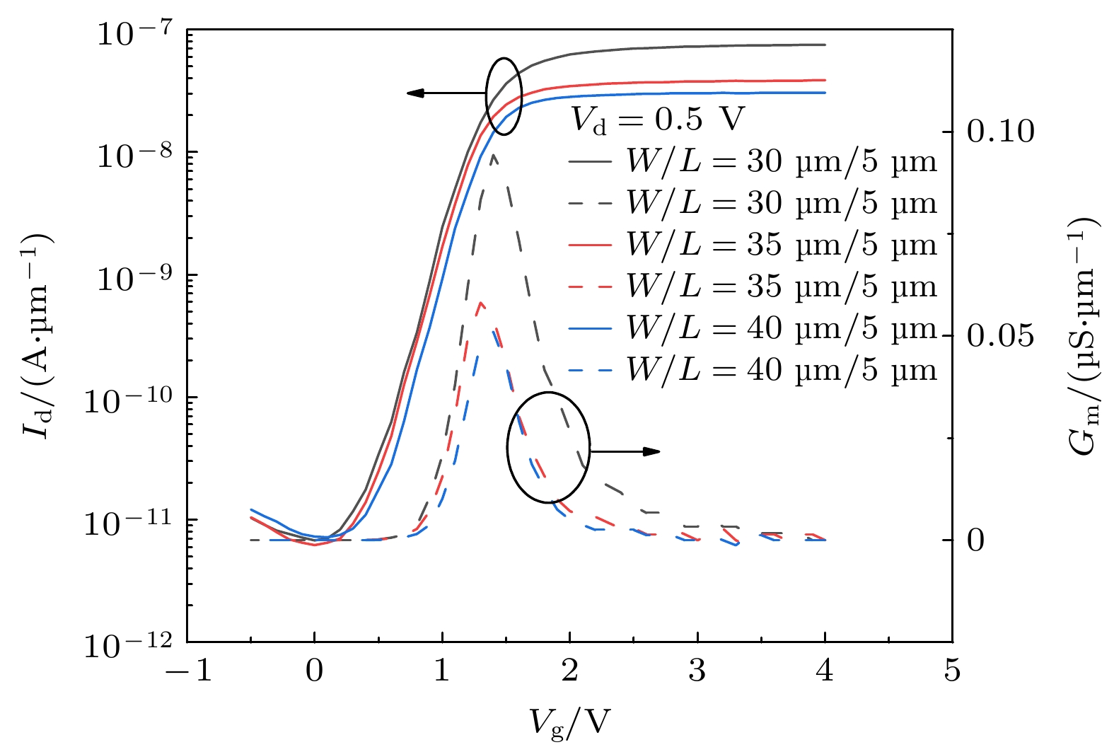
图 8 不同沟道尺寸的未辐照CNTFET归一化后的转移特性曲线与跨导
Fig. 8. Normalized transfer characteristic curves and transconductance of unirradiated CNTFET with different channel sizes.
表 1 N型和P型器件辐照前后电学参数变化量
Table 1. Changes in electrical parameters of N-type and P-type devices before and after irradiation.
器件类型 ΔGm/μS 标准差 ΔSS/(mV·dec–1) 标准差 ΔVth/mV 标准差 N型器件 –0.275 0.02 50 0.015 149 0.025 P型器件 –1 0.022 20 0.02 –45 0.018  下载: 导出CSV
表 2 辐照前后不同沟道尺寸的CNTFET电学参数变化
Table 2. Changes in electrical parameters of CNTFET with different channel sizes before and after irradiation.
宽长比 ΔGm/μS ΔSS/(mV·dec–1) ΔVth/V 30 µm/5 µm –0.34 52 0.15 35 µm/5 µm –0.35 53 0.19 40 µm/5 µm –0.65 60 0.7
下载: 导出CSV
-
[1] Qiu C G, Zhang Z Y, Xiao M M, Yang Y J, Zhong D L, Peng L M 2017 Science 355 271
Google Scholar
[2] Franklin A D, Luisier M, Han S J, Tulevski G, Breslin C M, Gignac L, Lundstrom M S, Haensch W 2012 Nano Lett. 12 758
Google Scholar
[3] Chen B Y, Zhang P P, Ding L, Han J, Qiu S, Li Q W, Zhang Z Y, Peng L M 2016 Nano Lett. 16 5120
Google Scholar
[4] Zhu M G, Si J, Zhang Z Y, Peng L M 2018 Adv. Mater. 30 1707068
Google Scholar
[5] Yang Y Y, Ding L, Chen H J, Han J, Zhang Z Y, Peng L M 2018 Nano Res. 11 300
Google Scholar
[6] Shulaker M M, Hills G, Patil N, Wei H, Chen H Y, Wong H S, Mitra S 2013 Nature 501 526
Google Scholar
[7] De Volder M F, Tawfick S H, Baughman R H, Hart A J 2013 Science 339 535
Google Scholar
[8] 刘一凡, 张志勇 2022 物理学报 71 068503
Google Scholar
Liu Y F, Zhang Z Y 2022 Acta Phys. Sin. 71 068503
Google Scholar
[9] 马武英, 陆妩, 郭旗, 何承发, 吴雪, 王信, 丛忠超, 汪波, 玛丽娅 2014 物理学报 63 026101
Google Scholar
Ma W Y, Lu W, Guo Q, He C F, Wu X, Wang X, Cong Z C, Wang B, Maria 2014 Acta Phys. Sin. 63 026101
Google Scholar
[10] 董世剑, 郭红霞, 马武英, 吕玲, 潘霄宇, 雷志锋, 岳少忠, 郝蕊静, 琚安安, 钟向丽, 欧阳晓平 2020 物理学报 69 078501
Google Scholar
Dong S J, Guo H X, Ma W Y, Lv L, Pan X Y, Lei Z F, Yue S Z, Hao R J, Ju A A, Zhong X L, Ouyang X P 2020 Acta Phys. Sin. 69 078501
Google Scholar
[11] Krasheninnikov A, Nordlund K, Sirviö M, Salonen, E, Keinonen J 2001 Phys. Rev. B 63 245405
Google Scholar
[12] Tolvanen A, Kotakoski J, Krasheninnikov A, Nordlund K 2007 Appl. Phys. Lett. 91 173109
Google Scholar
[13] Krasheninnikov A V, Nordlund K 2010 J. Appl. Phys. 107 071301
Google Scholar
[14] Zhao Y D, Li D Q, Xiao L, Liu J K, Xiao X Y, L G H, Jin Y H, Jiang K L, Wang J P, Fan S S, Li Q Q 2016 Carbon 108 363
Google Scholar
[15] Zhang X R, Zhu H P, Peng S A, Xiong G D, Zhu C Y, Huang X N, Cao S R, Zhang J J, Yan Y P, Yao Y, Zhang D Y, Shi J Y, Wang L, Li B, Jin Z 2021 J. Semicond. 42 112002
Google Scholar
[16] Zhu M G, Zhou J S, Sun P K, Peng L M, Zhang Z Y 2021 ACS Appl. Mater. Interfaces 13 47756
Google Scholar
[17] Kanhaiya P S, Yu A, Netzer R, Kemp W, Doyle D, Shulaker M M 2021 ACS Nano 15 17310
Google Scholar
[18] Petrosjanc K O, Adonin A S, Kharitonov I A, Sicheva M V 1994 Proceedings of 1994 IEEE International Conference on Microelectronic Test Structures Moscow, Russia, March 22–25, 1994 p126
[19] Oldham T R, Mclean F B 2002 IEEE T. Nucl. Sci. 50 483
[20] Galloway K F, Gaitan M, Russell T J 1984 IEEE T. Nucl. Sci. 31 1497
Google Scholar
[21] Lu P, Zhu M G, Zhao P X, Fan C W, Zhu H P, Gao J T, Y C, Han Z S, Li B, Liu J, Zhang Z Y 2023 ACS Appl. Mater. Interfaces 15 10936
Google Scholar
[22] McMorrow J J, Cress C D, Affouda C 2012 ACS Nano 6 5040
Google Scholar
[23] Belyakov V V, Pershenkov V S, Zebrev G I, Sogoyan A V, Chumakov A I, Nikiforov A Y, Skorobogatov P K 2003 Russian Microelectron. 32 25
Google Scholar
[24] Ni H Z, Li M, Li X H, Zhu X W, Liu H H, Xu M 2022 IEEE T. Electron Dev. 69 1069
Google Scholar
[25] Kim W, Javey A, Vermesh O, Wang Q, Li Y M, Dai H J, 2003 Nano Letters 3 193
Google Scholar
[26] Chua L L, Zaumseil J, Chang J F, Ou E C, Ho P K, Sirringhaus H, Friend R H 2005 Nature 434 194
Google Scholar
[27] Lee S, Koo B, Shin J, Lee E, Park H, Kim H 2006 Appl. Phys. Lett. 88 99
[28] Cai X, Gerlach C P, Frisbie C D 2007 J. Phys. Chem. C 111 452
Google Scholar
[29] Ha T J, Kiriya D, Chen K, Javey A 2014 ACS Appl. Mater. Interfaces 6 8441
Google Scholar
[30] Wang Y W, Wang S, Ye H D, Zhang W H, Xiang L 2023 IEEE T. Dev. Mater. Re. 23 571
Google Scholar

 下载:
下载:
计量
- 文章访问数: 2932
- PDF下载量: 82
- 被引次数: 0
