


-
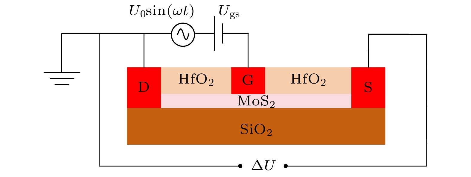
低维材料体系得益于其本身极高的载流子迁移率以及灵活的集成性, 在太赫兹探测领域被广泛研究并展现出极大的应用潜力. 目前利用软件对半导体太赫兹探测进行仿真分析所依赖的结构主要面向体材料, 而对于低维材料体系的太赫兹探测仿真分析则相对空白. 本文首次对单层MoS2场效应管中等离子体波效应的太赫兹探测进行了仿真分析, 并且系统地阐述了利用等离子体波进行太赫兹探测的原理以及分析过程. 通过调整不同的结构参数和外场条件, 该单层MoS2场效应管太赫兹探测器最大的直流电压信号输出可以达到14 μV. 该信号随着栅极与漏极之间的偏置电压呈现复杂的变化趋势, 通过研究发现该变化趋势与偏置电压引起的载流子浓度变化以及随之改变的动量弛豫时间相关. 本研究有望为低维材料太赫兹探测器设计提供进一步指导.Low-dimensional material systems benefit from their extremely high carrier mobility and flexible integrability, making them a subject of research in the terahertz detection field and demonstrating significant potential for applications. At present, software is mainly used to simulate and analyze the structures relied upon for semiconductor terahertz detection of bulk materials, while the simulation analysis for terahertz detection in low-dimensional material systems is still relatively unexplored. Due to the low degrees of freedom in carrier motion in low-dimensional materials, the probability of scattering caused by collisions between electrons and the lattice in the channel during electron movement is effectively reduced, making these materials have immense potential in high-sensitivity detection. Their low equivalent noise power and high signal-to-noise ratio performance in signal detection highlight the broad development prospects of these materials in the field of communication. This work simulates and analyzes the plasmon wave effect in a monolayer MoS2 field-effect transistor (FET) for THz detection for the first time, and systematically elucidates the principle and analysis process of using plasmon waves for THz detection. The transmission characteristic curve of the device is simulated and measured at a source-drain voltage of 0.5 V, and, a gate-to-drain voltage of –0.1 V is selected based on this curve to preliminarily investigate the THz response performance of the device. By adjusting key parameters such as Ugs, THz wave irradiation frequency, and HfO2 layer thickness, it is found that the monolayer MoS2 FET THz detector can produce a maximum DC voltage signal of 14 μV. This signal exhibits a complex variation trend related to the bias voltage between the gate and drain. This trend correlates with the bias voltage-induced changes in carrier concentration and the corresponding momentum relaxation time. The research results obtained in this paper can provide an important reference for designing low-dimensional material THz detectors. Furthermore, they lay a foundation for optimizing the performance of two-dimensional material THz detectors through simulation analysis, thereby providing deeper insights into the study of THz photoelectric responses in 2D materials.
-
Keywords:
- MoS2 /
- plasma wave /
- terahertz /
- TCAD simulation
[1] 冯伟, 韦舒婷, 曹俊诚 2021 物理学报 70 244303
 Google Scholar
Feng W, Wei S T, Cao J C 2021 Acta Phys. Sin. 70 244303
Google Scholar
[2] Wang C X, Wang J, Hu S, Jiang Z H, Tao J, Yan F 2021 IEEE Veh. Technol. Mag 16 27
Google Scholar
[3] Shafie A, Yang N, Han C, Jornet J M, Juntti M, Kürner T 2023 IEEE Network 37 162
Google Scholar
[4] Jiang W, Zhou Q H, He J G, Habibi M A, Melnyk S, El-Absi M, Han B, Renzo M D, Schotten H D, Luo F L, El-Bawab T S, Juntti M, Debbah M, Leung V C M 2024 IEEE Commun. Surv. Tutorials 26 2326
Google Scholar
[5] Liu Z L, Yang C, Peng M G 2024 IEEE Network 38 194
Google Scholar
[6] Chen W R, Li L X, Chen Z, Liu Y W, Ning B Y, Quek T Q S 2024 IEEE Trans. Veh. Technol. 73 19019
Google Scholar
[7] Han C, Wu Y Z, Chen Z, Chen Y, Wang G J 2024 IEEE Commun. Mag. 62 102
Google Scholar
[8] Taghinejad M, Xia C, Hrton M, Lee K T, Kim A S, Li Q, Guzelturk B, Kalousek R, Xu F, Cai W, Lindenberg A M, Brongersma M L 2023 Science 382 299
Google Scholar
[9] Mihnev M T, Kadi F, Divin C J, Winzer T, Lee S, Liu C H, Zhong Z, Berger C, de Heer W A, Malic E, Knorr A, Norris T B 2016 Nat. Commun. 7 11617
Google Scholar
[10] Zhang D H, Xu Z, Cheng G, Liu Z, Gutierrez A R, Zang W Z, Norris T B, Zhong Z H 2022 Nat. Commun. 13 6404
Google Scholar
[11] Krishna Kumar R, Li G, Bertini R, Chaudhary S, Nowakowski K, Park J M, Castilla S, Zhan Z, Pantaleón P A, Agarwal H, Batlle-Porro S, Icking E, Ceccanti M, Reserbat-Plantey A, Piccinini G, Barrier J, Khestanova E, Taniguchi T, Watanabe K, Stampfer C, Refael G, Guinea F, Jarillo-Herrero P, Song J C W, Stepanov P, Lewandowski C, Koppens F H L 2025 Nat. Mater. 24 1034
Google Scholar
[12] Dyakonov M, Shur M 1996 IEEE Trans. Electron Devices 43 380
Google Scholar
[13] Dyakonov M, Shur M 1993 Phys. Rev. Lett. 71 2465
Google Scholar
[14] Liu X Q, Shur M 2019 IEEE Radio and Wireless Symposium (RWS) Orlando, FL, USA, January 20−23, 2019 p1
[15] Liu X Q, Shur M S 2020 IEEE Trans. Terahertz Sci. Technol. 10 15
Google Scholar
[16] Meng Q Z, Lin Q J, Jing W X, Han F, Zhao M, Jiang Z D 2018 IEEE Trans. Electron Devices 65 4807
Google Scholar
[17] Zhu Y J, Ji X L, Liao Y M, Wu F W, Yan F 2014 12th IEEE International Conference on Solid-State and Integrated Circuit Technology (ICSICT) Guilin, China, October 28–31, 2014 p1
[18] Tong J Y, Muthee M, Chen S Y, Yngvesson S K, Yan J 2015 Nano Lett. 15 5295
Google Scholar
[19] Zhou J, Wang X Y, Chen Z Q Z, Zhang L B, Yao C Y, Du W J, Zhang J Z, Xing H Z, Fu N X, Chen G, Wang L 2022 Chin. Phys. B 31 050701
Google Scholar
[20] Shen J Z, Xing H Z, Wang L, Hu Z, Zhang L B, Wang X Y, Chen Z Q Z, Yao C Y, Jiang MJ, Fei F C, Chen G, Han L, Song F Q, Chen X S 2022 Appl. Phys. Lett. 120 063501
Google Scholar
[21] Shen Y, Tian H, Ren T L 2022 J. Semicond. 43 082002
Google Scholar
[22] Wang D, Yang L, Hu Z, Wang F, Yang Y G, Pan X K, Dong Z, Tian S J, Zhang L B, Han L, Jiang M J, Tang K Q, Dai F X, Zhang K, Lu W, Chen X S, Wang L, Hu W D 2025 Nat. Commun. 16 25
Google Scholar
[23] Han L, Zhang S, Tian S J, Zhang L B, Wei Y D, Zhang K X, Jiang M J, He Y, Liu C L, Tang W W, He J L, Shu H B, Politano A, Chen X S, Wang L 2025 ACS Nano 19 3740
Google Scholar
[24] Xiao K N, Zhang S, Zhang K X, Zhang L B, Wen Y F, Tian S J, Xiao Y L, Shi C F, Hou S C, Liu C L, Han L, He J L, Tang W W, Li G H, Wang L, Chen X S 2024 Adv. Sci. 11 2401716
Google Scholar
-
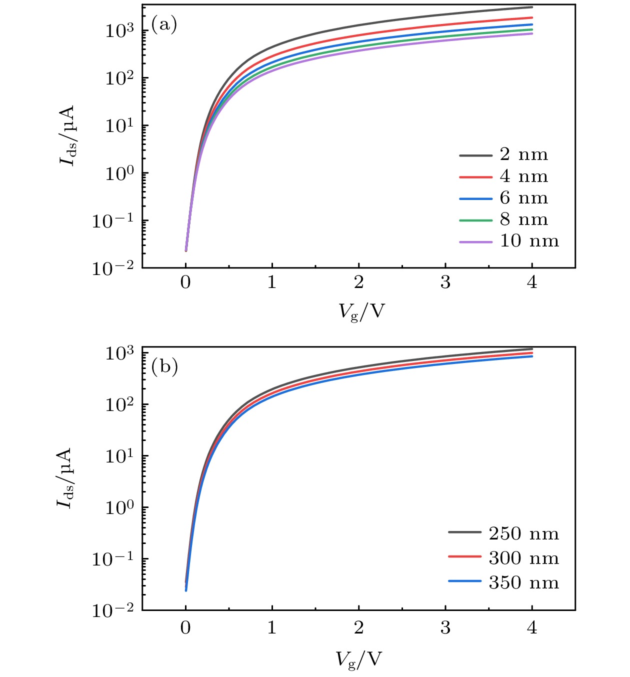
图 2 转移特性曲线 (a)不同HfO2厚度下的转移特性曲线; (b)不同沟道长度下的转移特性曲线
Fig. 2. Transfer characteristic curves: (a) The transfer characteristic curves with different HfO2 thickness; (b) the transfer characteristic curves with different channel length.
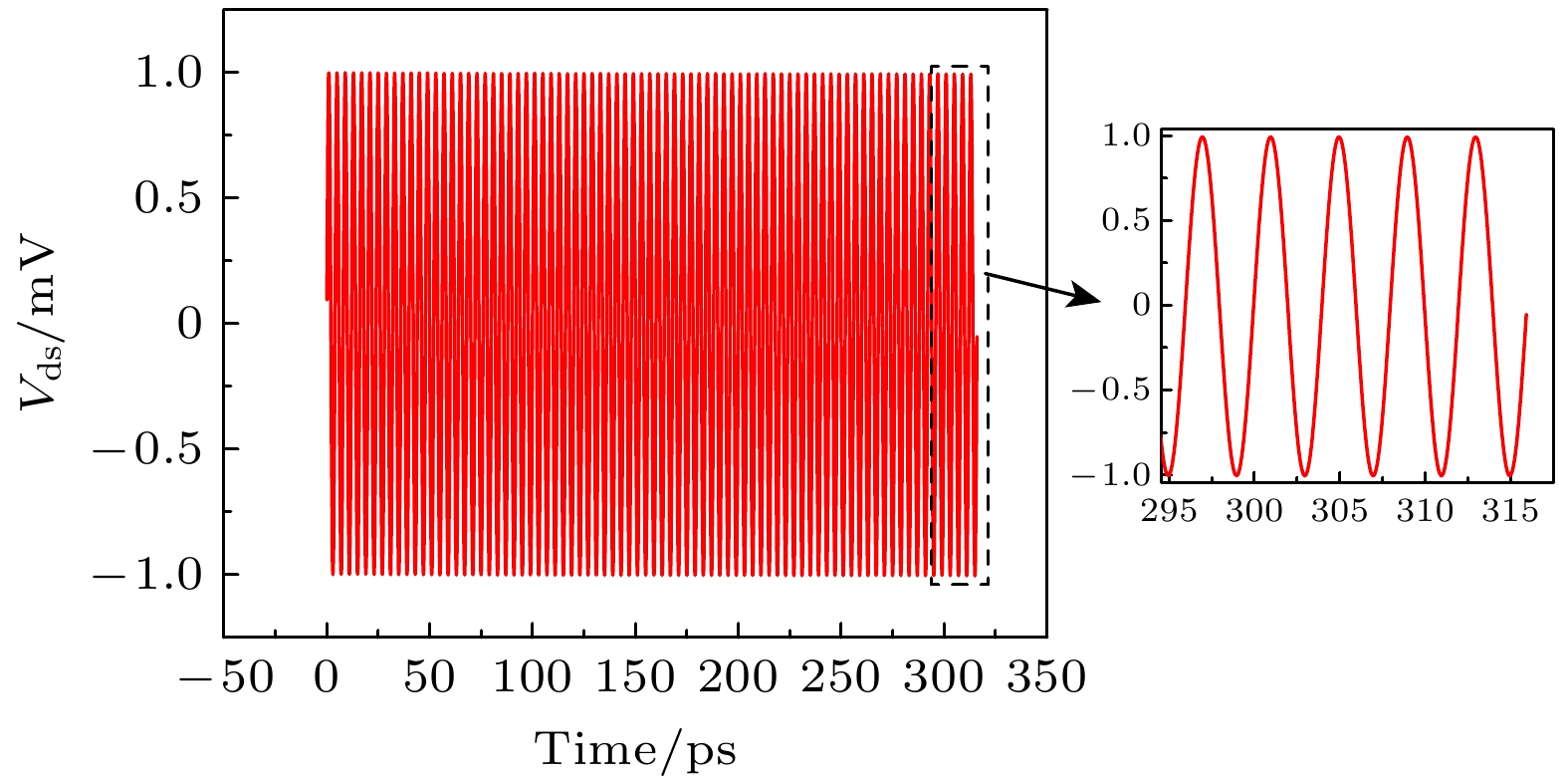
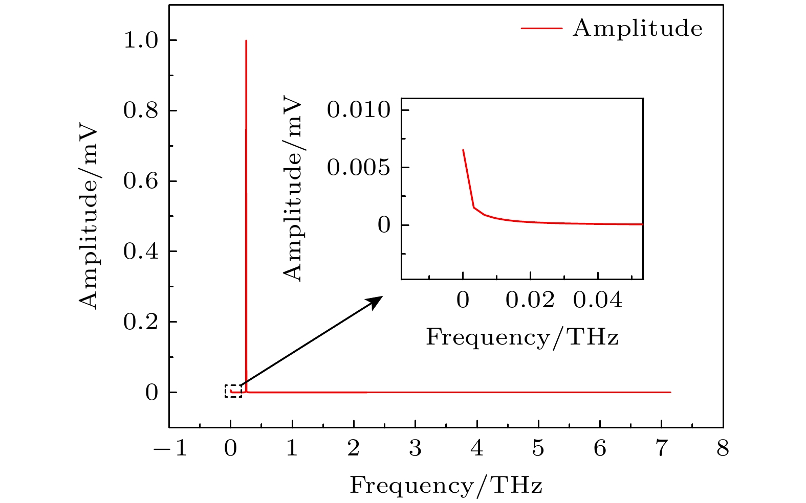
图 3 在太赫兹光激励下产生的源漏电压Vds随时间的关系
Fig. 3. Time domain of Vds stimulated by terahertz radiation.
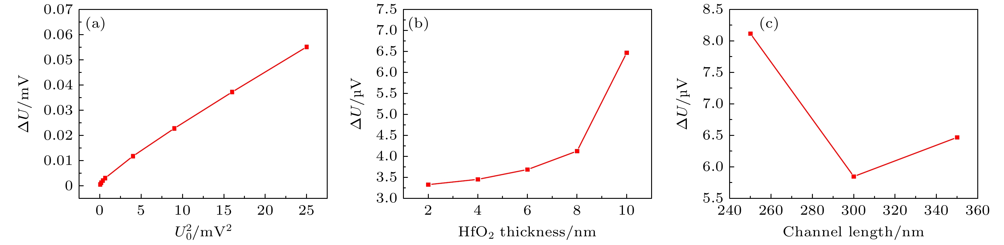
图 5 不同结构参数下的直流电压输出 (a) 不同太赫兹波振幅下的直流信号输出; (b)不同HfO2厚度下的直流信号输出; (c)不同沟道长度下的直流信号输出
Fig. 5. The DC voltages with different structure parameters: (a) The DC voltages with different U0; (b) the DC voltages with different HfO2 thicknesses; (c) the DC voltages with different channel lengths.
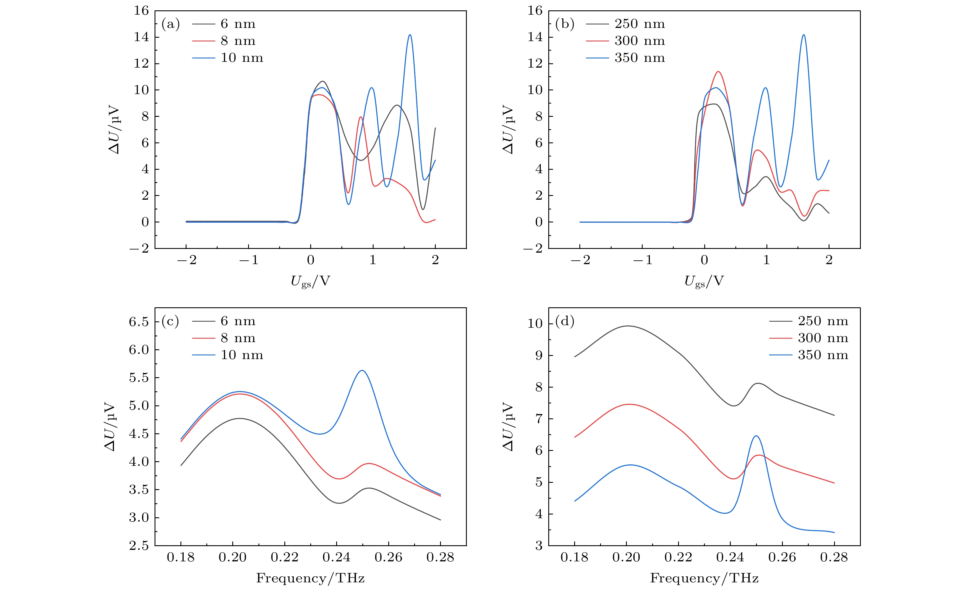
图 6 不同结构参数下直流电压信号随偏置电压以及频率的变化 (a), (b) 不同HfO2厚度(a)和不同沟道长度(b)结构的直流电压信号输出随着偏置电压的变化; (c), (d) 不同HfO2厚度(c)和不同沟道长度(d)结构的直流电压信号输出随着太赫兹波频率的变化
Fig. 6. The DC voltages with different structure parameters at different Ugs and terahertz frequencies: (a), (b) The variation of DC voltage signals with the bias voltage for structures with different HfO2 thicknesses (a) and different channel lengths (b); (c), (d) the variation of DC voltage signals with the frequency of terahertz waves for structures with different HfO2 thicknesses (c) and different channel lengths (d).
-
[1] 冯伟, 韦舒婷, 曹俊诚 2021 物理学报 70 244303
Google Scholar
Feng W, Wei S T, Cao J C 2021 Acta Phys. Sin. 70 244303
Google Scholar
[2] Wang C X, Wang J, Hu S, Jiang Z H, Tao J, Yan F 2021 IEEE Veh. Technol. Mag 16 27
Google Scholar
[3] Shafie A, Yang N, Han C, Jornet J M, Juntti M, Kürner T 2023 IEEE Network 37 162
Google Scholar
[4] Jiang W, Zhou Q H, He J G, Habibi M A, Melnyk S, El-Absi M, Han B, Renzo M D, Schotten H D, Luo F L, El-Bawab T S, Juntti M, Debbah M, Leung V C M 2024 IEEE Commun. Surv. Tutorials 26 2326
Google Scholar
[5] Liu Z L, Yang C, Peng M G 2024 IEEE Network 38 194
Google Scholar
[6] Chen W R, Li L X, Chen Z, Liu Y W, Ning B Y, Quek T Q S 2024 IEEE Trans. Veh. Technol. 73 19019
Google Scholar
[7] Han C, Wu Y Z, Chen Z, Chen Y, Wang G J 2024 IEEE Commun. Mag. 62 102
Google Scholar
[8] Taghinejad M, Xia C, Hrton M, Lee K T, Kim A S, Li Q, Guzelturk B, Kalousek R, Xu F, Cai W, Lindenberg A M, Brongersma M L 2023 Science 382 299
Google Scholar
[9] Mihnev M T, Kadi F, Divin C J, Winzer T, Lee S, Liu C H, Zhong Z, Berger C, de Heer W A, Malic E, Knorr A, Norris T B 2016 Nat. Commun. 7 11617
Google Scholar
[10] Zhang D H, Xu Z, Cheng G, Liu Z, Gutierrez A R, Zang W Z, Norris T B, Zhong Z H 2022 Nat. Commun. 13 6404
Google Scholar
[11] Krishna Kumar R, Li G, Bertini R, Chaudhary S, Nowakowski K, Park J M, Castilla S, Zhan Z, Pantaleón P A, Agarwal H, Batlle-Porro S, Icking E, Ceccanti M, Reserbat-Plantey A, Piccinini G, Barrier J, Khestanova E, Taniguchi T, Watanabe K, Stampfer C, Refael G, Guinea F, Jarillo-Herrero P, Song J C W, Stepanov P, Lewandowski C, Koppens F H L 2025 Nat. Mater. 24 1034
Google Scholar
[12] Dyakonov M, Shur M 1996 IEEE Trans. Electron Devices 43 380
Google Scholar
[13] Dyakonov M, Shur M 1993 Phys. Rev. Lett. 71 2465
Google Scholar
[14] Liu X Q, Shur M 2019 IEEE Radio and Wireless Symposium (RWS) Orlando, FL, USA, January 20−23, 2019 p1
[15] Liu X Q, Shur M S 2020 IEEE Trans. Terahertz Sci. Technol. 10 15
Google Scholar
[16] Meng Q Z, Lin Q J, Jing W X, Han F, Zhao M, Jiang Z D 2018 IEEE Trans. Electron Devices 65 4807
Google Scholar
[17] Zhu Y J, Ji X L, Liao Y M, Wu F W, Yan F 2014 12th IEEE International Conference on Solid-State and Integrated Circuit Technology (ICSICT) Guilin, China, October 28–31, 2014 p1
[18] Tong J Y, Muthee M, Chen S Y, Yngvesson S K, Yan J 2015 Nano Lett. 15 5295
Google Scholar
[19] Zhou J, Wang X Y, Chen Z Q Z, Zhang L B, Yao C Y, Du W J, Zhang J Z, Xing H Z, Fu N X, Chen G, Wang L 2022 Chin. Phys. B 31 050701
Google Scholar
[20] Shen J Z, Xing H Z, Wang L, Hu Z, Zhang L B, Wang X Y, Chen Z Q Z, Yao C Y, Jiang MJ, Fei F C, Chen G, Han L, Song F Q, Chen X S 2022 Appl. Phys. Lett. 120 063501
Google Scholar
[21] Shen Y, Tian H, Ren T L 2022 J. Semicond. 43 082002
Google Scholar
[22] Wang D, Yang L, Hu Z, Wang F, Yang Y G, Pan X K, Dong Z, Tian S J, Zhang L B, Han L, Jiang M J, Tang K Q, Dai F X, Zhang K, Lu W, Chen X S, Wang L, Hu W D 2025 Nat. Commun. 16 25
Google Scholar
[23] Han L, Zhang S, Tian S J, Zhang L B, Wei Y D, Zhang K X, Jiang M J, He Y, Liu C L, Tang W W, He J L, Shu H B, Politano A, Chen X S, Wang L 2025 ACS Nano 19 3740
Google Scholar
[24] Xiao K N, Zhang S, Zhang K X, Zhang L B, Wen Y F, Tian S J, Xiao Y L, Shi C F, Hou S C, Liu C L, Han L, He J L, Tang W W, Li G H, Wang L, Chen X S 2024 Adv. Sci. 11 2401716
Google Scholar

 下载:
下载:
计量
- 文章访问数: 1963
- PDF下载量: 42
- 被引次数: 0
