-
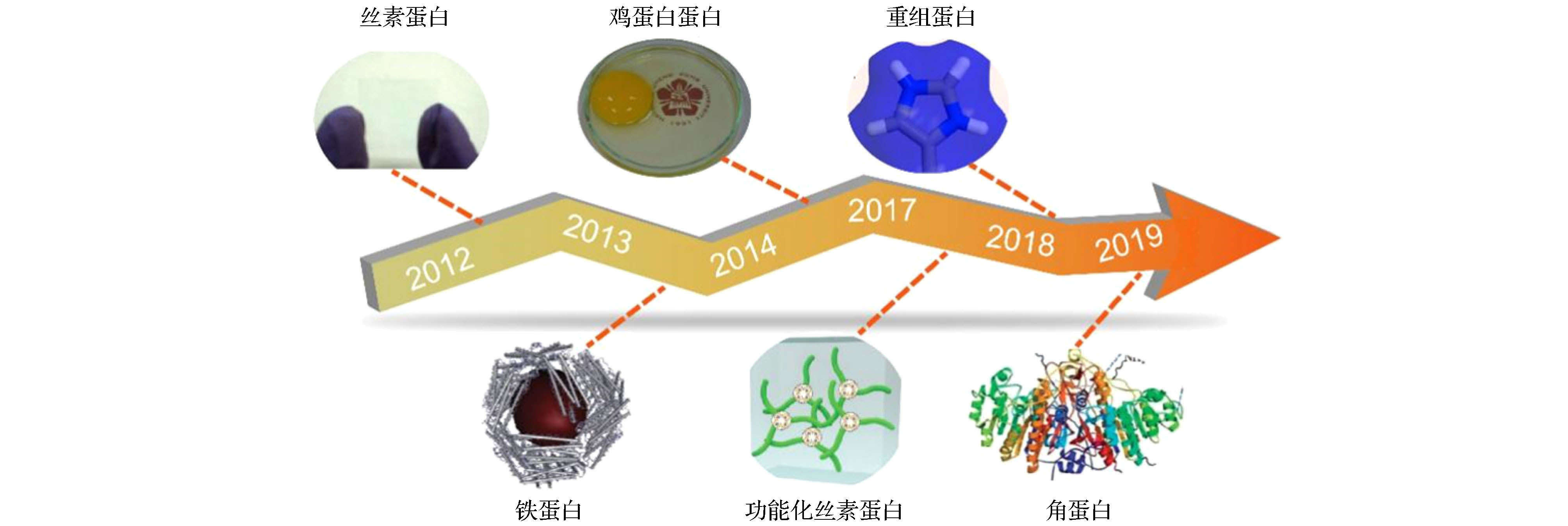
Memristor, as a new type of electronic component that can realize high density, multi-function, low power consumption, and multi-level data storage, has brought significant changes to the field of circuit structure design, information storage theory, and artificial synapses simulation. In a wide range of memristors, the protein-based memristors have unparalleled natural advantages in other cutting-edge information technology fields such as implantable computing, human-computer interaction, and human-computer integration due to their controllable degradation, rich and cheap raw materials, and biocompatibility. Therefore, the memristor is considered as the most potential candidate for building the next generation of high-tech information electronic device. In this article, the latest research progress of protein based memristors is comprehensively reviewed. The research progress of other proteins, including the widely studied egg albumen and artificial recombinant protein with excellent performance are first summarized, and then the research process of silk fibroin-based memristors, the performance improvement of silk fibroin-based memristors brought by functional strategies are comprehensively introduced. The Structure-activity relationship between structure and performance of functionalized silk fibroin is analyzed. Finally, the performance of the protein-based memristor is comprehensively analyzed, and the future development opportunities of the green electronic device are also prospected.
-
Keywords:
- mesoscopic functionalization /
- protein /
- memristor /
- electronic devices
[1] Borghetti J, Snider G S, Kuekes P J, Yang J J, Stewart D R, Williams R S 2010 Nature 464 873
 Google Scholar
[2] Strukov D B, Snider G S, Stewart D R, Williams R S 2008 Nature 453 80
 Google Scholar
[3] Wang M, Cai S, Pan C, Wang C, Lian X, Zhuo Y, Xu K, Cao T, Pan X, Wang B, Liang S J, Yang J J, Wang P, Miao F 2018 Nat. Electron. 1 130
 Google Scholar
[4] Zhou L, Mao J, Ren Y, Han S T, Roy V A L, Zhou Y 2018 Small 14 1703126
 Google Scholar
[5] Wang Z, Wang L, Nagai M, Xie L, Yi M, Huang W 2017 Adv. Electron. Mater. 3 1600510
 Google Scholar
[6] Yan X, Zhao J, Liu S, Zhou Z, Liu Q, Chen J, Liu X Y 2018 Adv. Funct. Mater. 28 1705320
 Google Scholar
[7] Yan X, Zhou Z, Zhao J, Liu Q, Wang H, Yuan G, Chen J 2018 Nano Research 11 1183
 Google Scholar
[8] Yan X, Wang J, Zhao M, Li X, Wang H, Zhang L, Lu C, Ren D 2018 Appl. Phys. Lett. 113 013503
 Google Scholar
[9] Yan X, Cao G, Wang J, Man M, Zhao J, Zhou Z, Wang H, Pei Y, Wang K, Gao C 2020 J. Mater. Chem. C 8 4926
 Google Scholar
[10] Lv Z, Zhou Y, Han S T, Roy V A L 2018 Mater. Today 21 537
 Google Scholar
[11] Pan F, Gao S, Chen C, Song C, Zeng F 2014 Mater. Sci. Eng. R 83 1
 Google Scholar
[12] Ji Y, Yang Y, Lee S K, Ruan G, Kim T W, Fei H, Lee S H, Kim D Y, Yoon J, Tour J M 2016 ACS Nano 10 7598
 Google Scholar
[13] Chang Y C, Wang Y H 2014 ACS Appl. Mater. Inter. 6 5413
 Google Scholar
[14] Goswami S, Matula A J, Rath S P, Hedstrom S, Saha S, Annamalai M, Sengupta D, Patra A, Ghosh S, Jani H, Sarkar S, Motapothula M R, Nijhuis C A, Martin J, Goswami S, Batista V S, Venkatesan T 2017 Nat. Mater. 16 1216
 Google Scholar
[15] Kim S, Jeong H Y, Kim S K, Choi S Y, Lee K J 2011 Nano Lett. 11 5438
 Google Scholar
[16] Lai Y C, Wang Y X, Huang Y C, Lin T Y, Hsieh Y P, Yang Y J, Chen Y F 2014 Adv. Funct. Mater. 24 1430
 Google Scholar
[17] Yan X, Zhao Q, Chen A P, Zhao J, Zhou Z, Wang J, Wang H, Zhang L, Li X, Xiao Z 2019 Small 15 1901423
 Google Scholar
[18] Yan X, Wang K, Zhao J, Zhou Z, Wang H, Wang J, Zhang L, Li X, Xiao Z, Zhao Q 2019 Small 15 1900107
 Google Scholar
[19] Zhou Z, Zhao J, Chen A P, Pei Y, Xiao Z, Wang G, Chen J, Fu G, Yan X 2020 Mater. Horiz. 7 1106
 Google Scholar
[20] Breivik K, Armitage J M, Wania F, Jones K C 2014 Environ. Sci. Technol. 48 8735
 Google Scholar
[21] Li Y, Xu X, Wu K, Chen G, Liu J, Chen S, Gu C, Zhang B, Zheng L, Zheng M, Huo X 2008 J. Environ. Monit. 10 1233
 Google Scholar
[22] Irimia Vladu M, Głowacki E D, Voss G, Bauer S, Sariciftci N S 2012 Mater. Today 15 340
 Google Scholar
[23] Zhou Z, Yan X, Zhao J, Lu C, Ren D, Lu N, Wang J, Zhang L, Li X, Wang H 2019 J. Mater. Chem. C 7 1561
 Google Scholar
[24] Shi C, Wang J, Sushko M L, Qiu W, Yan X, Liu X Y 2019 Adv. Funct. Mater. 29 1904777
 Google Scholar
[25] Zhu B, Wang H, Leow W R, Cai Y, Loh X J, Han M Y, Chen X 2016 Adv. Mater. 28 4250
 Google Scholar
[26] Zhou G, Ren Z, Wang L, Sun B, Duan S, Song Q 2019 Mater Horiz 6 1877
 Google Scholar
[27] Chen Y C, Yu H C, Huang C Y, Chung W L, Wu S L, Su Y K 2015 Sci. Rep. 5 10022
 Google Scholar
[28] Qiu W, Patil A, Hu F, Liu X Y 2019 Small 15 1903948
 Google Scholar
[29] He X, Zhang J, Wang W, Xuan W, Wang X, Zhang Q, Smith C G, Luo J 2016 ACS Appl. Mater. Inter 8 10954
 Google Scholar
[30] Sun B, Zhang X, Zhou G, Li P, Zhang Y, Wang H, Xia Y, Zhao Y 2017 Org. Electron. 42 181
 Google Scholar
[31] Kim S U, Yagati A K, Min J, Choi J W 2010 Biomaterials 31 1293
 Google Scholar
[32] Yan X, Li X, Zhou Z, Zhao J, Wang H, Wang J, Zhang L, Ren D, Zhang X, Chen J, Lu C, Zhou P, Liu Q 2019 ACS Appl. Mater. Inter 11 18654
 Google Scholar
[33] Wang H, Meng F, Cai Y, Zheng L, Li Y, Liu Y, Jiang Y, Wang X, Chen X 2013 Adv. Mater. 25 5498
 Google Scholar
[34] Zhang C, Shang J, Xue W, Tan H, Pan L, Yang X, Guo S, Hao J, Liu G, Li R W 2016 Chem. Commun. 52 4828
 Google Scholar
[35] Moudgil A, Kalyani N, Sinsinbar G, Das S, Mishra P 2018 ACS Appl. Mater. Inter 10 4866
 Google Scholar
[36] Sun B, Liang D, Li X, Chen P 2015 J. Mater. Sci. Mater. Electron. 27 3957
[37] Poul Nissen J H, Nenad Ban, Peter B. Moore, Thomas A. Steitz 2000 Science 289 920
 Google Scholar
[38] Johnson E, Cascio D, Sawaya M R, Gingery M, Schröder I 2005 Structure 13 637
 Google Scholar
[39] Meng F, Sana B, Li Y, Liu Y, Lim S, Chen X 2014 Small 10 277
 Google Scholar
[40] Yongmin Ko Y K, Hyunhee Baek, and Jinhan Cho 2011 ACS Nano 5 9918
 Google Scholar
[41] Jang S K, Kim S, Salman M S, Jang J R, Um Y M, Tan L, Park J H, Choe W S, Lee S 2018 Chem. Mater. 30 781
 Google Scholar
[42] Debabov V G 2004 Mol. Biol. 38 578
[43] Khaleghi M, Kermanshahi R K, Yaghoobi M, Zarkesh Esfahani S, Baghizadeh A 2010 J. Microbiol. Biotechnol. 20 749
[44] Howorka S, Sára M, Wang Y, Kuen B, Sleytr U B, Lubitz W, Bayley H 2000 J. Biol. Chem. 275 37876
 Google Scholar
[45] Iturri J, Vianna A C, Moreno Cencerrado A, Pum D, Sleytr U B, Toca Herrera J L 2017 Beilstein J. Nanotechnol. 8 91
 Google Scholar
[46] Sára M, Sleytr U B 2000 J. Bacteriol. 182 859
 Google Scholar
[47] Baek H, Lee C, Lim K I, Cho J 2012 Nanotechnology 23 155604
 Google Scholar
[48] Ko J, Nguyen L T H, Surendran A, Tan B Y, Ng K W, Leong W L 2017 ACS Appl. Mater. Inter 9 43004
 Google Scholar
[49] Singh R, Lin Y T, Chuang W L, Ko F H 2017 Org. Electron. 44 198
 Google Scholar
[50] Lin Q, Hao S, Hu W, Wang M, Zang Z, Zhu L, Du J, Tang X 2019 J. Mater. Chem.C 7 3315
 Google Scholar
[51] Idris A, Vijayaraghavan R, Rana U A, Patti A F, MacFarlane D R 2014 Green Chem. 16 2857
 Google Scholar
[52] Bhushan B 2008 Prog. Mater. Sci. 53 585
 Google Scholar
[53] Reddy N, Hu C, Yan K, Yang Y 2011 Mater. Sci. Eng. C 31 1706
 Google Scholar
[54] Rouse J G, Van Dyke M E 2010 Materials 3 999
 Google Scholar
[55] Guo B, Sun B, Hou W, Chen Y, Zhu S, Mao S, Zheng L, Lei M, Li B, Fu G 2019 Rsc Adv. 9 12436
 Google Scholar
[56] Tu H, Yu R, Lin Z, Zhang L, Lin N, Yu W D, Liu X Y 2016 Adv. Funct. Mater. 26 9032
 Google Scholar
[57] Lin N, Cao L, Huang Q, Wang C, Wang Y, Zhou J, Liu X Y 2016 Adv. Funct. Mater. 26 8885
 Google Scholar
[58] Chen Z, Zhang H, Lin Z, Lin Y, van Esch J H, Liu X Y 2016 Adv. Funct. Mater. 26 8978
 Google Scholar
[59] Song Y, Lin Z, Kong L, Xing Y, Lin N, Zhang Z, Chen B H, Liu X Y 2017 Adv. Funct. Mater. 27 1700628
 Google Scholar
[60] Shi C, Xing Y, Patil A, Meng Z, Yu R, Lin N, Qiu W, Hu F, Liu X Y 2019 ACS Appl. Mater. Inter. 11 30125
 Google Scholar
[61] Hota M K, Bera M K, Kundu B, Kundu S C, Maiti C K 2012 Adv. Funct. Mater. 22 4493
 Google Scholar
[62] Mukherjee C, Hota M K, Naskar D, Kundu S C, Maiti C K 2013 Phys. Status Solidi A 210 1797
 Google Scholar
[63] Wang H, Du Y, Li Y, Zhu B, Leow W R, Li Y, Pan J, Wu T, Chen X 2015 Adv. Funct. Mater. 25 3825
 Google Scholar
[64] Wang H, Zhu B, Wang H, Ma X, Hao Y, Chen X 2016 Small 12 3360
 Google Scholar
[65] Wang H, Zhu B, Ma X, Hao Y, Chen X 2016 Small 12 2715
 Google Scholar
[66] Kook G, Jeong S, Kim M K, Lee S, Choi N, Lee H J 2020 Adv. Mater. Technol. 5 1900991
 Google Scholar
[67] Lin N, Liu X Y 2015 Chem. Soc. Rev. 44 7881
 Google Scholar
[68] Xing Y, Shi C, Zhao J, Qiu W, Lin N, Wang J, Yan X B, Yu W D, Liu X Y 2017 Small 13 1702390
 Google Scholar
[69] Lv Z, Wang Y, Chen J, Wang J, Zhou Y, Han S T 2020 Chem. Rev. 120 3941
 Google Scholar
[70] Lv Z, Wang Y, Chen Z, Sun L, Wang J, Chen M, Xu Z, Liao Q, Zhou L, Chen X, Li J, Zhou K, Zhou Y, Zeng Y J, Han S T, Roy V A L 2018 Adv. Sci. 5 1800714
 Google Scholar
[71] Lv Z, Chen M, Qian F, Roy V A L, Ye W, She D, Wang Y, Xu Z X, Zhou Y, Han S T 2019 Adv. Funct. Mater. 29 1902374
 Google Scholar
[72] Gogurla N, Mondal S P, Sinha A K, Katiyar A K, Banerjee W, Kundu S C, Ray S K 2013 Nanotechnology 24 345202
 Google Scholar
[73] Murgunde B K, Rabinal M K 2017 Org. Electron. 48 276
 Google Scholar
[74] Yong J, Hassan B, Liang Y, Ganesan K, Rajasekharan R, Evans R, Egan G, Kavehei O, Li J, Chana G, Nasr B, Skafidas E 2017 Sci. Rep. 7 14731
 Google Scholar
[75] Zhu J X, Zhou W L, Wang Z Q, Xu H Y, Lin Y, Liu W Z, Ma J G, Liu Y C 2017 Rsc Adv. 7 32114
 Google Scholar
[76] Yan X, Pei Y, Chen H, Zhao J, Zhou Z, Wang H, Zhang L, Wang J, Li X, Qin C 2019 Adv. Mater. 31 1805284
 Google Scholar
[77] Yan X, Zhang L, Chen H, Li X, Wang J, Liu Q, Lu C, Chen J, Wu H, Zhou P 2018 Adv. Funct. Mater. 28 1803728
 Google Scholar
[78] Yang J J, Strukov D B, Stewart D R 2013 Nat. Nanotechnol. 8 13
 Google Scholar
-
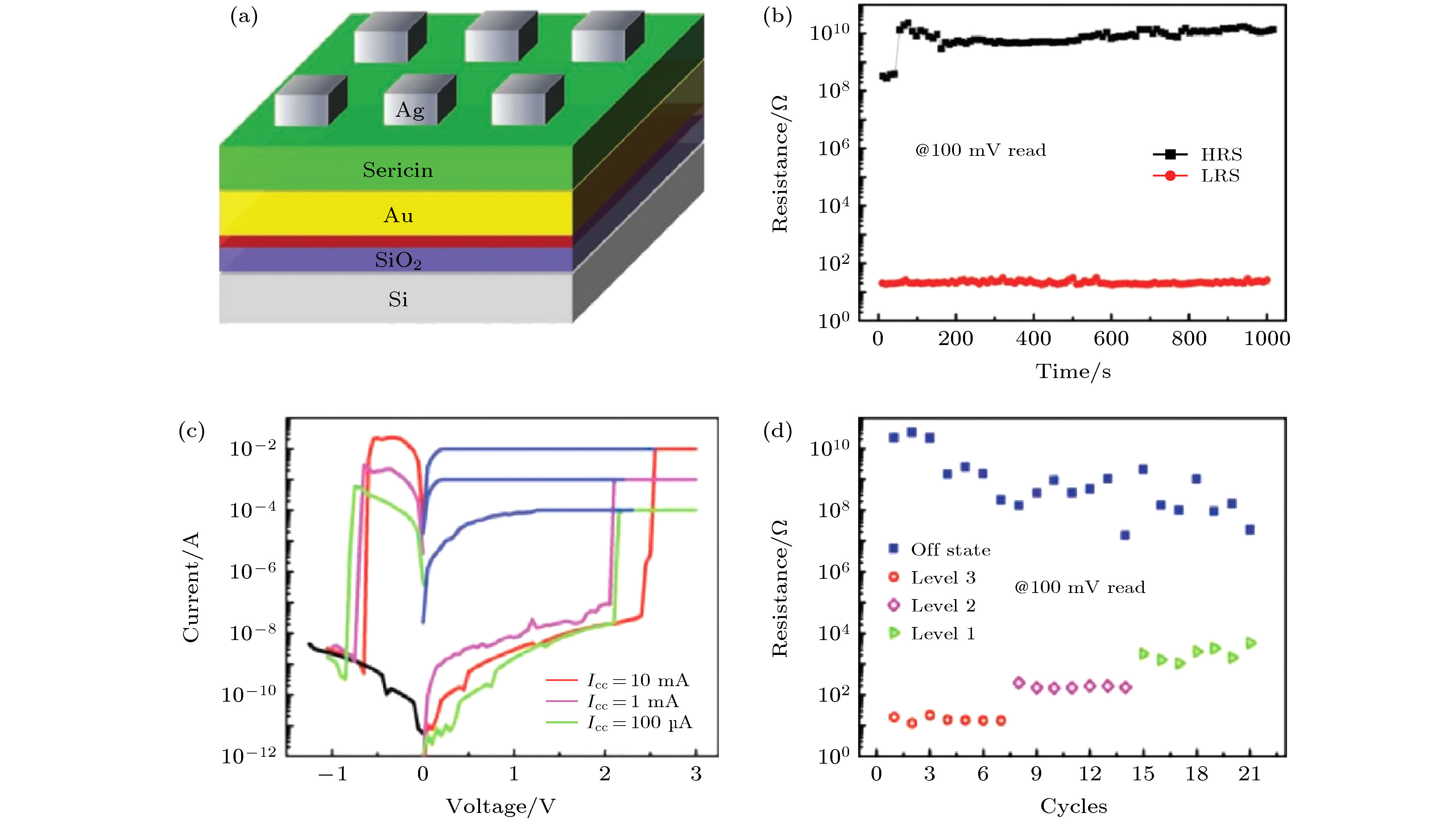
图 2 (a) 丝胶蛋白基忆阻器的器件结构示意图; (b) 器件的保持特性; (c) 不同限定电流下的I-V循环性能; (d) 不同限定电流下的高低阻态分布[33]
Figure 2. (a) Schema of sericin memristor; (b) the retention characteristics of the device; (c) typical I-V curves of the device under different compliance currents; (d) the resistance of the device with different compliance currents[33].
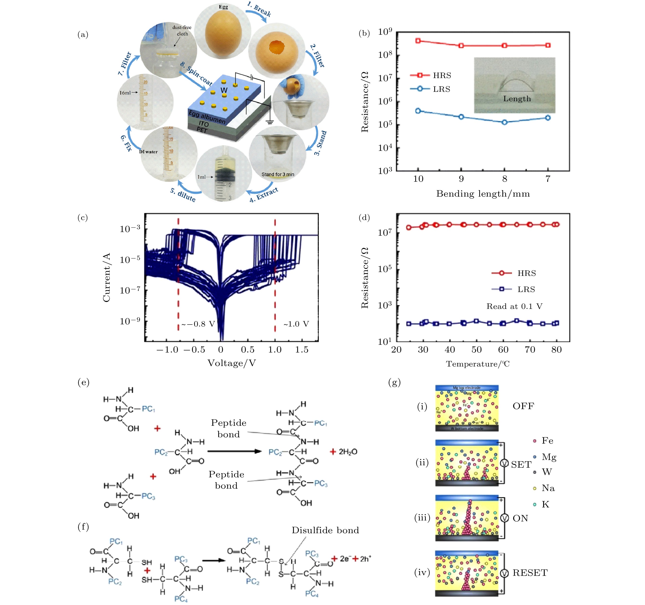
图 3 鸡蛋白蛋白基忆阻器 (a) W/鸡蛋白蛋白/ITO/PET忆阻器的制造工艺和原理图; (b) 器件高低阻态与弯曲长度的关系; (c) 来自同一阵列的3个不同忆阻器单元的I-V曲线的叠加; (d) 正向偏压下忆阻器在不同温度下的高低阻态值分布; 具有不同蛋白质链的氨基酸之间的(e)肽键和(f)二硫键合成的一般方案; (g) 蛋白质基忆阻器的四个切换过程的示意图: (i)忆阻器的初始状态, 其中金属Mg和金属W分别作为顶部和底部电极, 彩色球体代表不同的离子; (ii)当施加正电压后, 顶部电极上的离子沿着电场移动, 并在蛋白层的强电场区域中局部聚集; (iii)同时从底部电极注入的电子还原金属离子(例如Fe3+和Mg2+)形成金属元素. 在特定的电压下, 形成导电细丝以连接顶部和底部电极, 然后开启设备低阻态(LRS); (iv)当施加关闭电压时, 导电丝由于金属元素被来自顶部电极的注入电子氧化而在顶部电极附近断裂, 器件逐渐返回到高阻态(HRS)[29,32]
Figure 3. Schema of egg albumen memristor: (a) Proposed fabrication process and schematic of a W/egg albumen/ITO/PET memristor; (b) extracted device HRS and LRS versus bending length; (c) superposition of I-V curves for 3 different memristor cells from the same cross-bar array measured 15 times each; (d) the HRS and LRS resistances of a memristor cell under different temperature with positive bias; general of scheme of peptide bonds (e) and disulfide bonds (f) synthesis between amino acids with different protein chains; (g) schematic drawings of the four switching processes for an albumen-based memristor: (i) Initial state of a memristor with Mg and W as the top and bottom electrode, respectively. The colorful spheres represent different ions; (ii) when a positive voltage is applied to the top electrode, ions move along the electric field, and accumulate locally in strong field regions in the albumen layer; (iii) meanwhile injected electrons from the bottom electrode reduce metallic ions such as Fe3+ and Mg2+ to metal elements. At a specific voltage, the filaments are formed to connect the top and bottom electrodes electrically, and the device is turned on, i.e. the LRS; (iv) when applying a reset voltage, the conductive filaments are broken due to the oxidation of the metal elements by the injected electrons from the top electrode, the filaments are ruptured near the top electrode and the device gradually returns to the HRS[29,32].
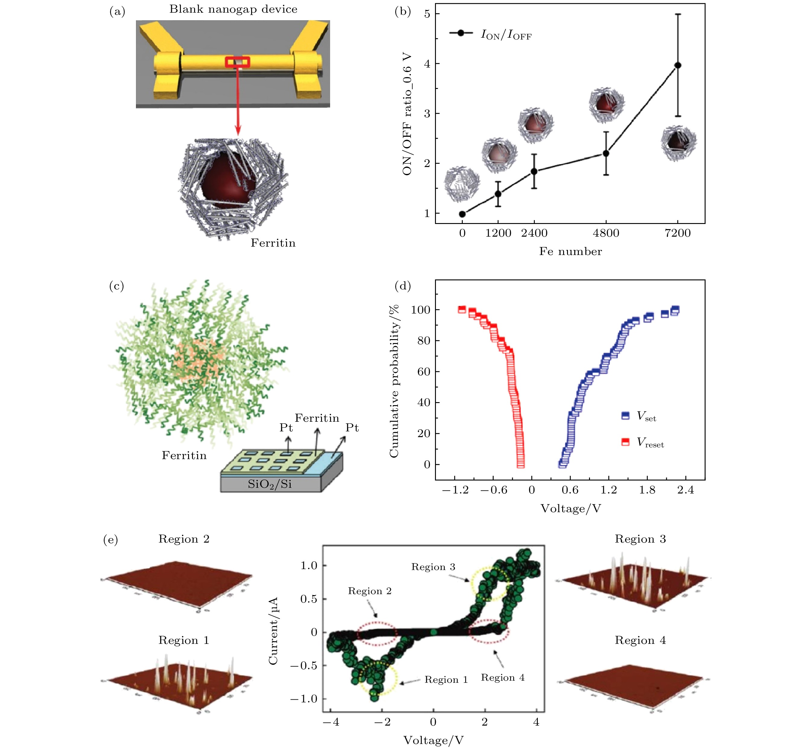
图 4 铁蛋白基忆阻器 (a) 一种单根纳米棒器件的器件结构示意图, 该器件的铁蛋白纳米笼放置在光刻产生的约12 nm的间隙里; (b) 基于铁蛋白的纳米忆阻器件的开关比与铁负荷载量的关系(蛋白质纳米核的颜色强度表示铁原子的密度大小); (c) 铁蛋白基忆阻器的原理图及铁蛋白结构示意图, 铁蛋白由肽单元(绿色)外壳和水合氧化铁(橙色)组成的矿物核心组成; (d) 非易失性存储器的开关电压分布; (e) (PAH/铁蛋白)3多层器件的I-V曲线和导电原子力显微镜(C-AFM)图像 从各个区域测量多层器件的C-AFM图像, 证实了导电丝状路径的形成. 分别是正电压扫描期间(ON(区域3)和OFF状态(区域4)以及反向扫描下的(ON(区域1)和OFF(区域2)状态). 通过C-AFM表征, 将电化学惰性的Pt尖端代替Ag电极用作顶部电极. 在“SET”过程(即从OFF切换到ON状态)和“RESET” (即从高电流(ON)切换)之后, 观察到随机分布路径的形成和破裂[34,39,40]
Figure 4. Ferritin based memristor: (a) Illustration of the fabrication of a single nanorod device with ferritin nanocage spanning OWL-generated about 12 nm gap; (b) ON/OFF ratio of ferritin-based memristive nanodevices with different Fe loading (the color intensity of the protein nanocage core indicates the density of Fe atom); (c) schematic diagram of ferritin, the spherical shell consists of peptide subunits (green) and the mineral core consisting of hydrous iron oxide (orange), lower right panel is the schematic illustration of the Pt/ferritin/Pt memristor on the SiO2/Si substrate; (d) switching voltage distributions of the non-volatile memory; (e) I-V curve and CS-AFM images of (PAH/ferritin)3 multilayers in the ON (Region 3) and OFF state (Region 4) during positive voltage sweep, and the ON (Region 1) and OFF (Region 2) state during negative voltage sweep, respectively. CS-AFM images of multilayer devices were measured from the respective regions in the I-V curve of a (PAH/ferritin)3 multilayer device. The formation of conductive filamentary paths was confirmed by CS-AFM characterizations. In this case, an electrochemically inert Pt tip was used as a top electrode instead of the Ag electrode. The formation and rupture of the randomly distributed paths were observed after “SET” processes (i.e., switching from low-current (OFF) to high-current (ON) state) and “RESET” (i.e., switching from high-current (ON) to low-current (OFF) state)[34,39,40].
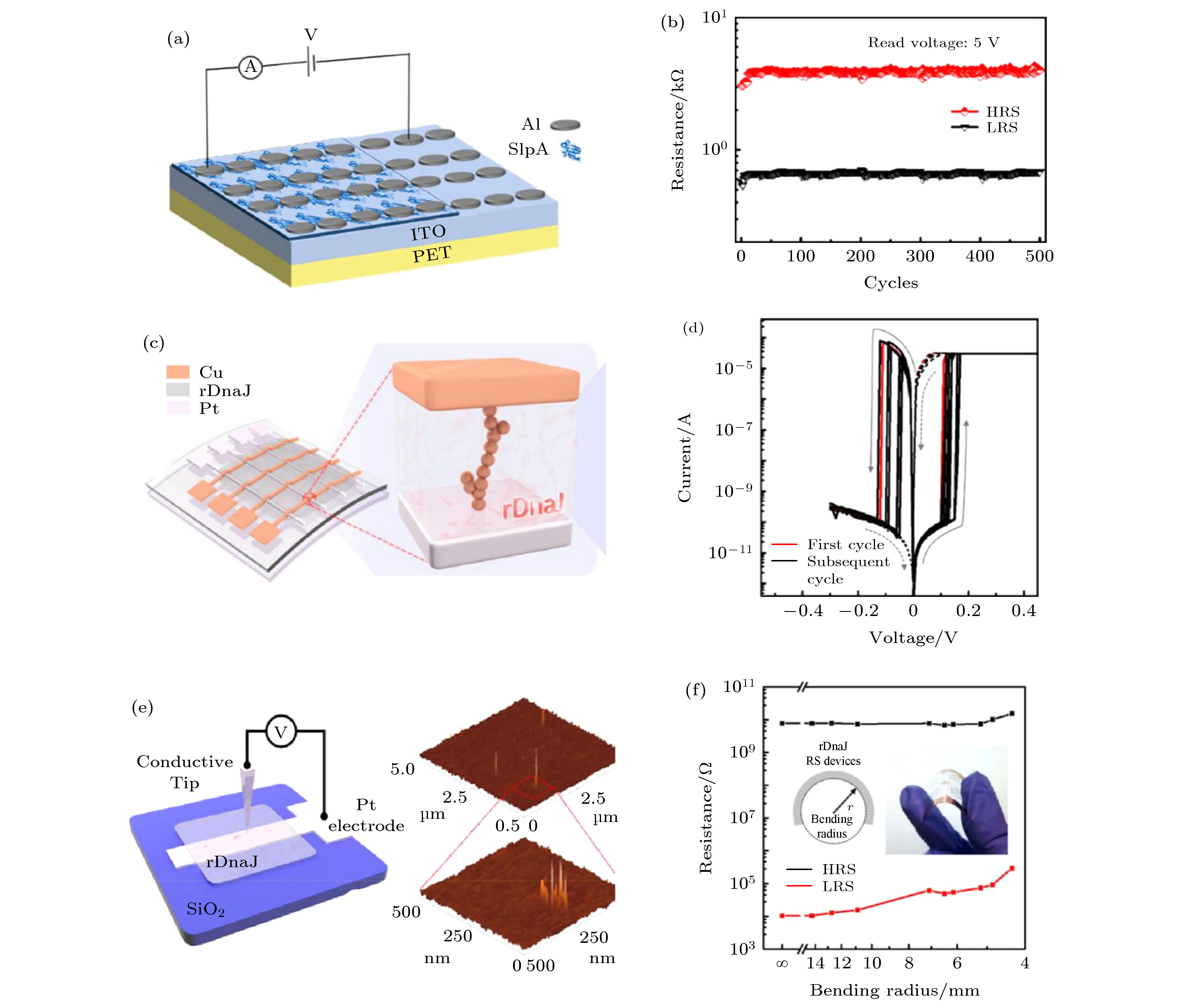
图 5 (a) S-layer蛋白基忆阻器的器件结构示意图; (b) 器件的循环稳定性; (c) 重组蛋白rDnaJ基忆阻器的器件结构示意图; (d) 器件I-V循环曲线; (e) 用于观察导电细丝的导电原子力显微镜测试原理图及相应的电流映射图像; (f) 重组蛋白基忆阻器的柔性性能, 在不同弯曲曲率下的阻值分布[35,41]
Figure 5. (a) Schema of S-layer protein memristor; (b) endurance characteristics; (c) schematic diagrams of the fabricated rDnaJ device arrays; (d) I-V characteristics of the rDnaJ based memristor; (e) schematic diagram of the CAFM used to observe the conductive filaments. CAFM current mapping image of a conductive filament in the rDnaJ-device after removing the top Cu electrode. The inset shows an enlarged CAFM image of the indicated area; (f) resistance as a function of bending radius for the rDnaJ device fabricated on the flexible PET substrate[35,41].
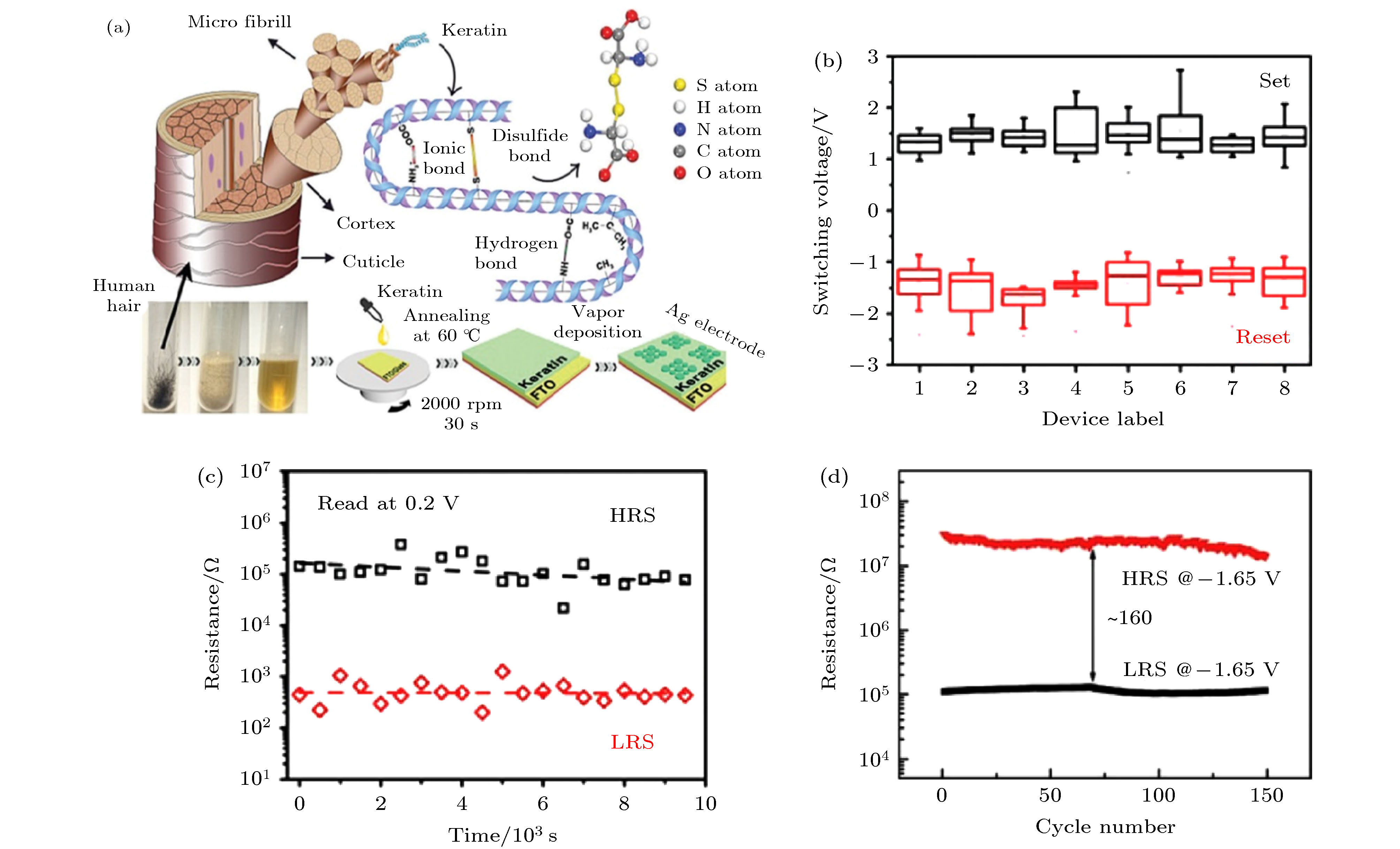
图 6 (a) 人发角蛋白结构及相应忆阻器的器件结构示意图; (b) 器件的开关电压分布; (c) 器件的保持特性; (d) 器件可稳定循环150次[50,55]
Figure 6. (a) Schematic diagrams of keratin from human hair, and the fabrication process of Ag/keratin/FTO memory devices; (b) set and reset voltage distributions collected from eight different devices; (c) the retention characteristics of the device; (d) distribution of the HRS and LRS over 150 consecutive cycles[50,55].
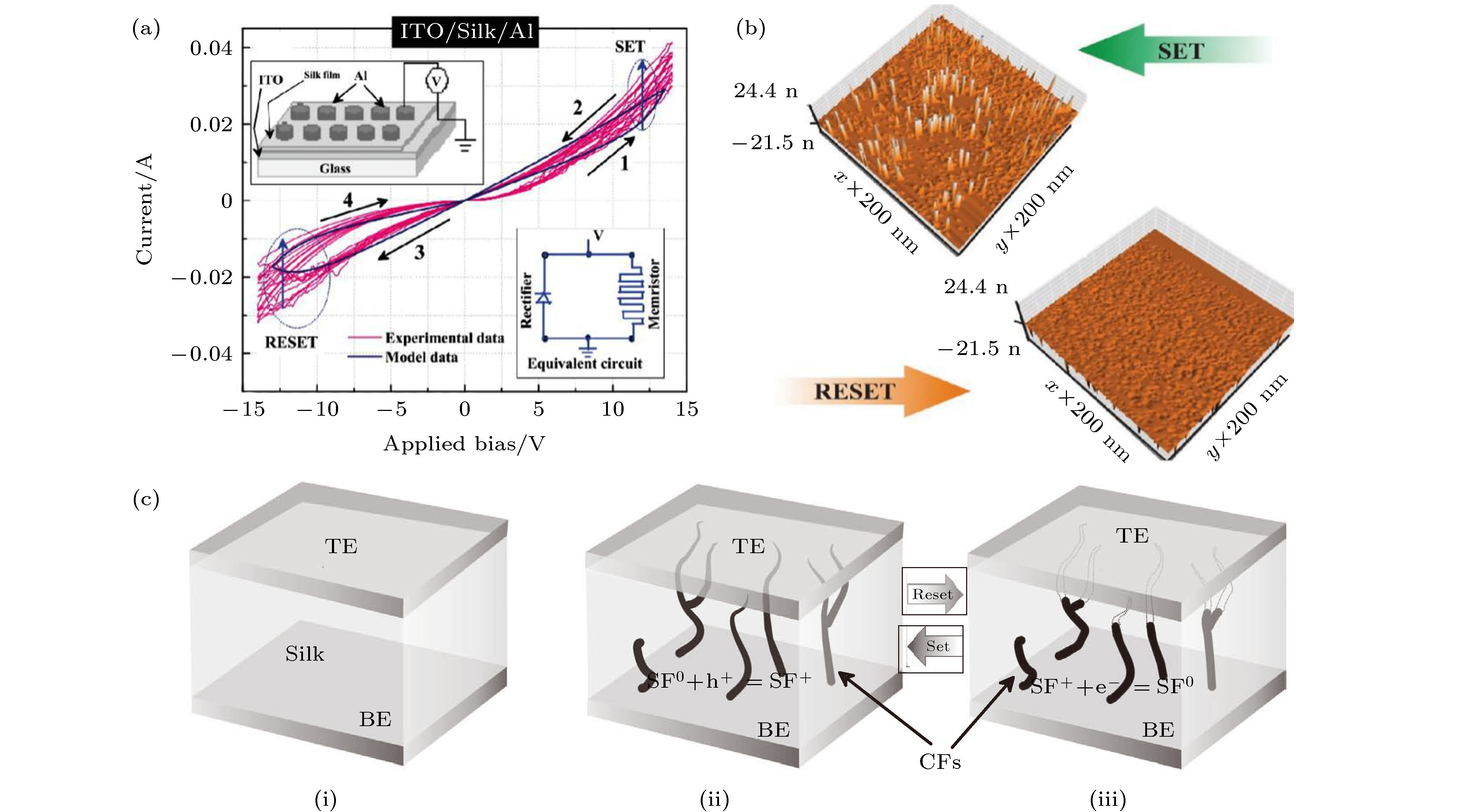
图 7 Hota课题组[61]所构建的蚕丝蛋白材料基忆阻器 (a) 蚕丝蛋白基忆阻器的I-V特性, 其中插图的上图展示的是装配好的忆阻器器件的原理图, 下图显示其等效电路模型, 该电路由与忆阻器并联的整流器组成; (b) 蚕丝蛋白基忆阻器在SET和RESET条件下的纳米级电导率映射, 扫描隧道显微镜图像显示在SET条件下, 高密度的导电斑点或导电丝形成, 而在RESET条件下, 导电斑点或导电丝消失; (c) 用以解释蚕丝蛋白基忆阻器开关机制的物理模型: (i) 原始设备条件, 即在施加任何偏压之前, (ii) 在正偏压下达到SET条件时, 在SET状态, 当发生局部氧化(SF+)且密度达到临界值时, 发生软击穿(soft breakdown)以形成渗滤路径, (iii) 通过负偏置实现复位条件. 由于导电SF+路径断裂, 该设备返回到新的HRS
Figure 7. Silk fibroin-based memristors prepared by Hota’s research group[61]: (a) The I-V characteristics of silk fibroin-based memristors. The corresponding schematic of fabricated memristor device is shown in upper inset. The equivalent circuit model consists of a rectifier in parallel with a memristor is shown in lower inset. (b) Nanoscale conductivity mapping of silk fibroin based memristors under SET and RESET conditions. The STM image shows a higher density of conducting spots or conducting filaments formation during SET condition while those disappear during RESET condition. (c) Proposed physical to explain the switching mechanism of silk fibroin based memristors: (i) Original device conditions, before any bias is applied. (ii) Forming/SET condition is achieved with positive bias. During SET condition local oxidation (SF+) takes place and a soft breakdown event occurs when the density of SF+ reaches a critical value such that a percolation path is formed. (iii) A reset condition is achieved by negative bias. As the conductive SF+ path breaks, the device returns to its fresh-like HRS.
图 8 蚕丝蛋白材料基忆阻器 (a) 蚕丝蛋白基忆阻器的器件结构示意图; (b) 该蚕丝蛋白基忆阻器的I-V特性曲线; (c) 器件相应的保持特性; (d) 可由一根头发维持的2 cm × 2 cm大小的忆阻器照片展示; (e) 该轻质蚕丝蛋白基忆阻器的I-V特性曲线; (f) 器件相应的保持特性; (g) 瞬态蚕丝蛋白基忆阻器的器件结构示意图, 由于Mg具有良好的生物相容性, 可溶于水和生理环境, 因此选择Mg作为电极; (h), (i) 室温下, 存储设备在DI水中溶解的时间序列; (j) 单个蚕丝蛋白基存储器单元在12 × 12阵列单元中的扫描电镜图像, 单个蚕丝蛋白图案夹在底部和顶部电极之间; (k) 制成的忆阻器阵列在1.3 mm的曲率半径的圆柱体上滚动图示; (l) 蚕丝蛋白薄膜阵列的I-V特性[63-66]
Figure 8. The silk fibroin based memristor: (a) Model of silk fibroin based memristor; (b) I-V characteristic curve of the silk fibroin based memristor; (c) the corresponding retention characteristics of the device; (d) the photograph display of a 2 cm × 2 cm memristor that can be sustained by a human hair; (e) I-V characteristic curve of the light silk fibroin-based memristor; (f) the corresponding retention characteristics of the device; (g) schematic of the transient resistive switching memory device, Mg has good biocompatibility and is soluble in water and physiological environment; (h), (i)time sequence of dissolution of the memory devices in DI water at room temperature; (j) scanning electron microscope image of a single silk fibroin-based memory cell in a 12 × 12 array cell, a single silk fibroin pattern is sandwiched between the bottom and top electrodes; (k) the fabricated memristor array is scrolled on a cylinder with a radius of curvature of 1.3 mm; (l) I-V characteristics of silk fibroin arrays[63-66].
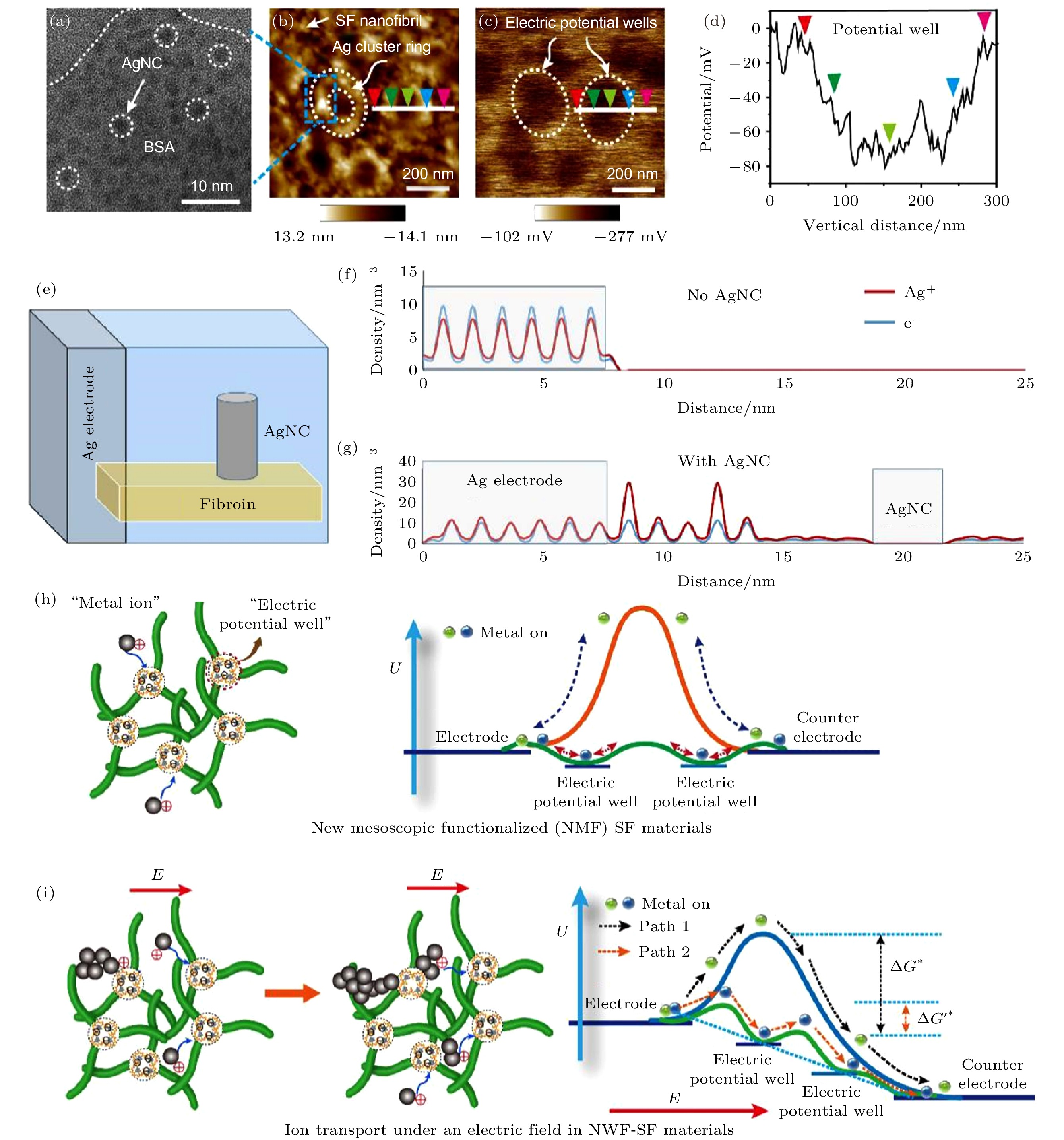
图 9 介观材料中的电子传递 (a) AgNCs @ BSA的TEM图像, 显示银纳米簇尺寸为3—4 nm; 银纳米簇功能化的蚕丝蛋白材料的原子力显微镜图像(b)和表面电势图像(c), 电子阱(纳米环区域)的尺寸为200 nm, 并且由于表面上电子的积累, 电势要低得多 (施加的电压为500 mV, 尖端与样品之间的间隙为100 nm); (d) 相应的电势; (e) Poisson-Nernest-Planck模拟; (f) 无AgNC和(g) 有AgNC时的稳态Ag离子和电子密度分布; (h) 新型介观功能化蚕丝蛋白材料结构模型(左侧)与金属离子迁移势垒(右侧); (i) 在电场作用下新型介观功能化蚕丝蛋白材料的离子传输路径(左图)和相应的离子传输路径图示(右侧). 分别是克服金属离子迁移高势垒(∆G*)(路径1, 蓝色曲线)和低势垒(∆G'*)(路径2, 绿色曲线)的两条路径[24]
Figure 9. Scheme of electron transport in mesoscopic materials: (a) TEM image of AgNCs@BSA showing a core size of 3−4 nm. AFM topographic image (b) and KPFM image (c) of a AgNC (white circles)-functionalized SF film, the electronic wells (b) are 200 nm in size and (c) have a much lower electric potential due to the accumulation of electrons at the surface, the nano seeds (AgNCs) is 30% (the applied voltage is 500 mV, and the gap between the tip and the sample is 100 nm); (d) the corresponding electric potential; (e) the simulation of Poisson-Nernest-Planck; steady state Ag ion and electron density distributions without (f) and with (g) AgNC; (h) scheme of new mesoscopic functionalized SF materials (left side) and the barrier of metal ion migration (right side); (i) scheme of ion transport under an electric field in new mesoscopic functionalized SF materials (left side) and the corresponding schema of different ion transport paths (right side). Two paths to overcome a high potential barrier of metal ion migration (∆G*) (path 1, blue curve) and a lower potential barrier (∆G'*) (path 2, green curve)[24].
图 10 Liu课题组[68]利用介观功能化策略所构建的Au掺杂蚕丝蛋白基介观忆阻器 (a) 功能化蚕丝蛋白基忆阻器的器件结构示意图; (b) 功能化蚕丝蛋白基忆阻器的I-V特性曲线, 可实现100次稳定循环; (c) 未功能化蚕丝蛋白基忆阻器的I-V特性曲线; (d), (e) Au功能化掺杂后蚕丝蛋白薄膜的表面电势原子力扫描照片, 可以看出Au纳米簇的引入, 使得蚕丝蛋白薄膜表面出现低电势区域; (f) 器件降解图示, 使用木瓜蛋白酶, 可以实现蚕丝蛋白基忆阻器件的可控降解; (g) 功能化蚕丝蛋白基忆阻器的导电丝生长路径解析, Au纳米簇的功能组装到蚕丝蛋白的介观网络中, 引导导电丝的生长, 使得导电丝生长变的有序可控
Figure 10. Mesoscopic functionalization strategies were used to construct Au-doped silk fibroin-based memristors by Liu's group[68]: (a) Schema of meso-functionalized silk memristor; (b) the 100 times I-V curve of Ag/WK@AuNCs-silk fibroin/ITO, measured by applying voltage to the top Ag electrode while keeping the ITO bottom electrode grounded; (c) the I-V curve of the Ag/neat-silk fibroin/ITO device; (d), (e) the electric potential images of a silk fibroin film functionalized by WK@AuNCs (dot line circles), a much lower electric potential due to the accumulation of electrons at the surfaces (the applied voltage: 500 mV, and the gap between the tip and the sample: 100 nm); (f) the WK@AuNCs-silk fibroin memristor was dissolved completed by the papain solution while the one in water was stable; (g) schema of the conduction mechanism of the Ag/WK@AuNCs-silk fibroin/ITO device. Ag ions move from the Ag electrode through the silk fibroin film toward the ITO electrode with the assistance of the AuNCs. Ag ions bridged by the AuNCs are reduced in the ITO electrode.
图 11 介观掺杂蚕丝蛋白基忆阻器电学性能 (a) 基于蚕丝蛋白材料的存储设备的典型I-V特性, 电阻通过“开启”过程从HRS切换到 LRS; (b) 未功能化和(c)功能化蚕丝蛋白基忆阻器的I-V曲线; (d) 未功能化(蓝色)和功能化(黄色)器件的阻态分布; (e) 未功能化(蓝色)和功能化(黄色)器件的开启和关闭电压的分布. (f) 开关电压和开关比的分布与银纳米簇掺杂量的关系; (g), (h) 介观功能化器件擦写速度; (i) 不同有机存储介质的工作电压比较, 与未功能化蚕丝蛋白忆阻器相比, 介观功能化的蚕丝蛋白基忆阻器的开启/关闭电压降低了约40倍(从12.0 V到0.3 V); (j) 比较不同类别存储介质的写入/擦除速度, 与其他报道的蛋白质基忆阻器相比, 介观功能化的蚕丝蛋白基忆阻器的写入/擦除速度提高了约10倍(从100 ns到10 ns)[24]
Figure 11. Electronic characteristics of meso-devices: (a) Typical current-voltage (I-V) characteristics of silk fibroin-based memory devices, the resistance switches from the HRS to LRS through a “set” process, and the state can be reversed via a “reset” step; I-V curves of (b) Ag0 and (c) Ag30; (d) distribution of the resistance of neat silk fibroin (blue) and functionalized silk fibroin (yellow) devices at the HRS and LRS; (e) distribution of the set and reset voltages in neat silk fibroin (blue) and functionalized silk fibroin (yellow) devices; (f) the distributions of Vset, Vreset, and OFF/ON ratio as a function of the amount of Ag used to functionalize the switching layer; switching speed of the functionalized silk fibroin memristor, the write/erase speeds are (g) 15 ns and (h) 10 ns, respectively; (i) comparison of operating voltages for different organic storage media. The set/reset voltage of the meso-functionalized silk fibroin memristor is reduced about 40 times (from 12 to 0.3 V) compared with the neat silk fibroin memristor; (j) comparison of write/erase speeds for different categories of storage media. The write/erase speed of the meso-functionalized silk fibroin memristor is improved about 10 times (from 100 to 10 ns) compared with other reported protein memristors[24].
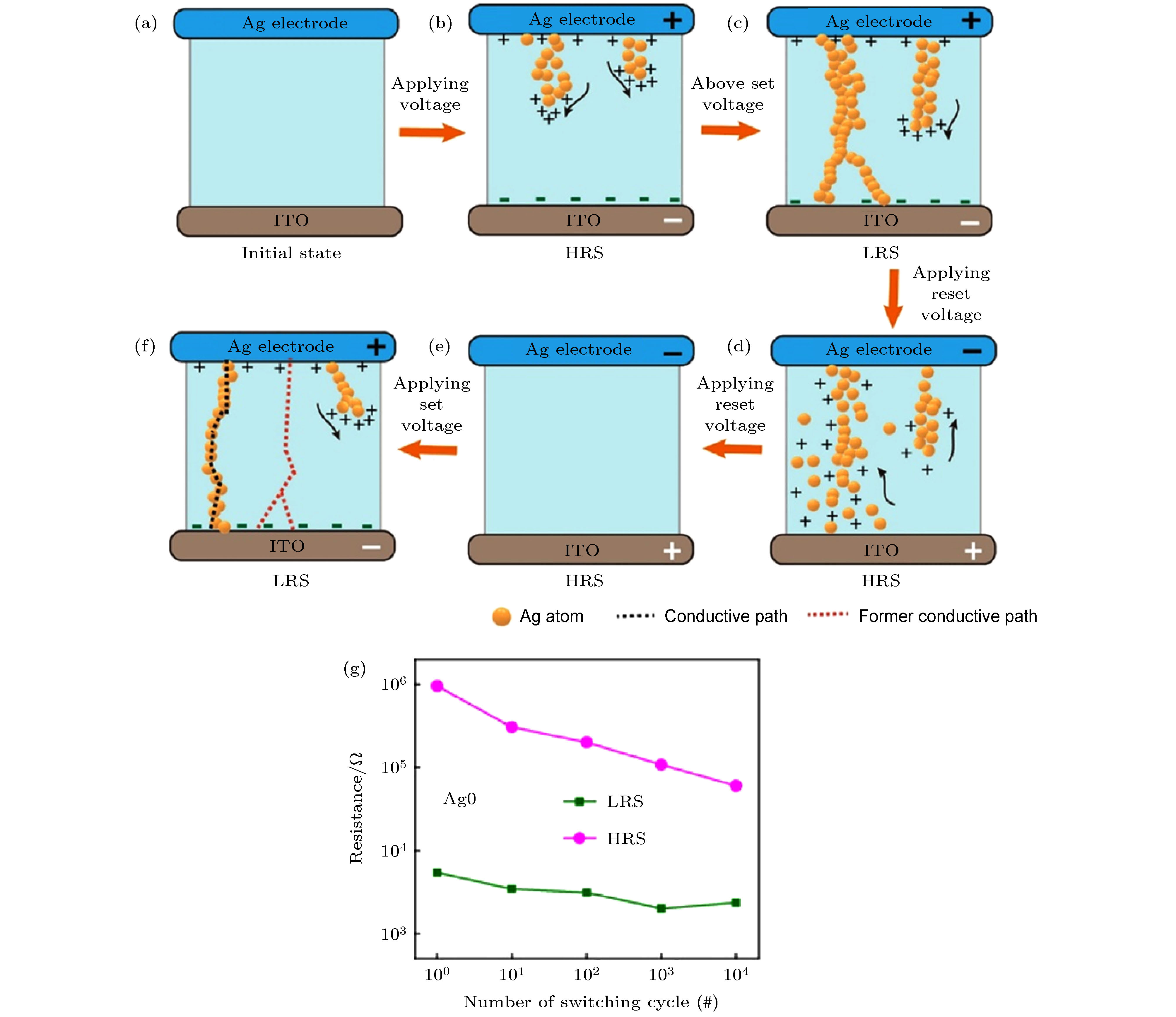
图 12 纯蚕丝蛋白基忆阻器阻变机制示意图 (a) 初始状态; (b) 对应正扫描时的高阻态; (c) 低阻态下的导电细丝; (d) 当施加关闭电压时, 器件切换到高阻态, 对应于导电丝的断裂; (e) 对应的反向扫描时的高阻态; (f) 电场作用下, 后续反复扫描所形成的随机导电丝; (g) 纯蚕丝蛋白基忆阻器的耐久周期[24]
Figure 12. Schematic structure diagrams illustrating resistances switching mechanism in the pure SF memristor: (a) Initial state; (b) HRS state during corresponding positive sweeps; (c) LRS state, conductive filaments are formed in LRS state during corresponding set sweeps; (d) the device switches to HRS when applied reset voltage corresponds to rupture of the conductive filaments; (e) HRS state during corresponding negative sweeps; (f) the random conductive filaments formed in subsequent repeated sweeps under an electric field; (g) endurance cycles of neat SF memristor[24].
图 13 介观功能化器件开关机制的原理示意图 (a) 电阻状态变化过程中所对应的I-V测试图; (b) 电阻状态变化过程中所对应的导电细丝生长动力学示意图, 图中红色的银团簇代表阻变材料中的介观功能化区域; 当外部电场极化时, 这些团簇可以作为正电荷势阱, 其中(i) 初始状态, (ii) 对应正扫描时的高阻状态, (iii) 在低阻状态下形成导电丝, (iv) 当开始施加的反向电压时, 导电细丝溶解, 器件保持为低阻态, (v) 当施加的反向电压达到关闭电压时, 器件切换到高阻态, 关闭电压对应于导电细丝的断裂, (vi)对应的反向扫描时的高阻态. 在随后的电场描中依然形成有序的导电细丝; (c)介观功能化蚕丝蛋白基忆阻器的耐久周期[24]
Figure 13. Schematic structure diagrams illustrating the resistance switching mechanism in AgNC meso-functionalized devices. (a) Current-voltage diagrams representing the resistance state during step-by-step changes in the electric field. (b) Schematic of filament growth dynamics corresponding to the resistance state. The red Ag clusters in the schematic represent mesoscopic functionali-zation in the memristive material; these clusters can act as a positive charge trap when polarized by an external electric field. The arrows indicate the switching direction: (i) Initial state; (ii) HRS state during corresponding positive sweeps; (iii) LRS state, conductive filaments are formed in the LRS state during corresponding set sweeps; (iv) the device remains in the LRS when the applied reverse voltage corresponds to the dissolution of the conductive filaments; (v) the device switches to the HRS when the applied reverse voltage reaches the reset voltage, which corresponds to the rupture of the conductive filaments; (vi) HRS state during corresponding negative sweeps. Well-organized conductive filaments are formed in subsequent repeated sweeps under an electric field. (c) Endurance cycles of Meso-functionalized silk fibroin memristor[24].
图 14 碳点掺杂蚕丝蛋白基忆阻器 (a) 器件结构的横截面扫描电镜图像; (b) 碳点的透射电镜图像; (c) 碳点-蚕丝蛋白功能掺杂薄膜在云母衬底上的原子力显微镜形貌图; (d) 器件的I-V特性, 暴露于紫外照射下(λ = 365 nm), 曝光强度从0到0.15 MW/cm2; (e) 器件开启电压的分布, 左图无紫外处理, 右图经过紫外曝光; (f) 器件开启操作后薄膜中导电丝的扫描电镜的图像和不同区域的能谱图; (g) Au/并五苯-碳点-蚕丝蛋白/SiO2/Si器件设备的横截面扫描电镜图像; (h) 碳点-蚕丝蛋白功能掺杂薄膜的原子力显微图像; (i) 在黑暗和紫外光照情况下的存储器输出特性; (j) 在黑暗(左图)和紫外线(右图)照射下, 通过施加在探针针尖上的递增电压进行电子注入后的碳点-蚕丝蛋白功能掺杂薄膜的开尔文表面电势原子力显微镜图像; (k) 相应选择区域的表面电势值[70,71]
Figure 14. Carbon dots(CDs)-doped silk fibroin-based memristors: (a) Cross-sectional SEM image of the device structure; (b) TEM images of pristine CDs; (c) AFM topographic images of CDs-silk composite film on a mica substrate, scale bar is 300 nm; (d) Ag top electrode, exposed to UV light (λ = 365 nm) with intensity from 0 to 0.15 Mw/cm2 (sweeping rate is 50 mV); (e) distribution of SET voltages without (left) and with (right) UV light treatment; (f) an enlarged SEM image of the conductive filament and EDS spectra in different regions; (g) cross-sectional SEM image of the Au/pentacene/CDs/silk/SiO2/Si device; (h) AFM topographic images of the CDs/silk bicomponent blend film; (i) output characteristics of the memory under dark conditions (left panel) and light illumination (right panel, λ = 365 nm, light intensity: 0.15 Mw/cm2); (j) KPFM image of CDs/silk film after electrons injection through incrementally increasing voltage applied to the tip under dark (left panel) and under UV illumination (right panel); (k) the CPD value of the selected cross sections in (j)[70,71].
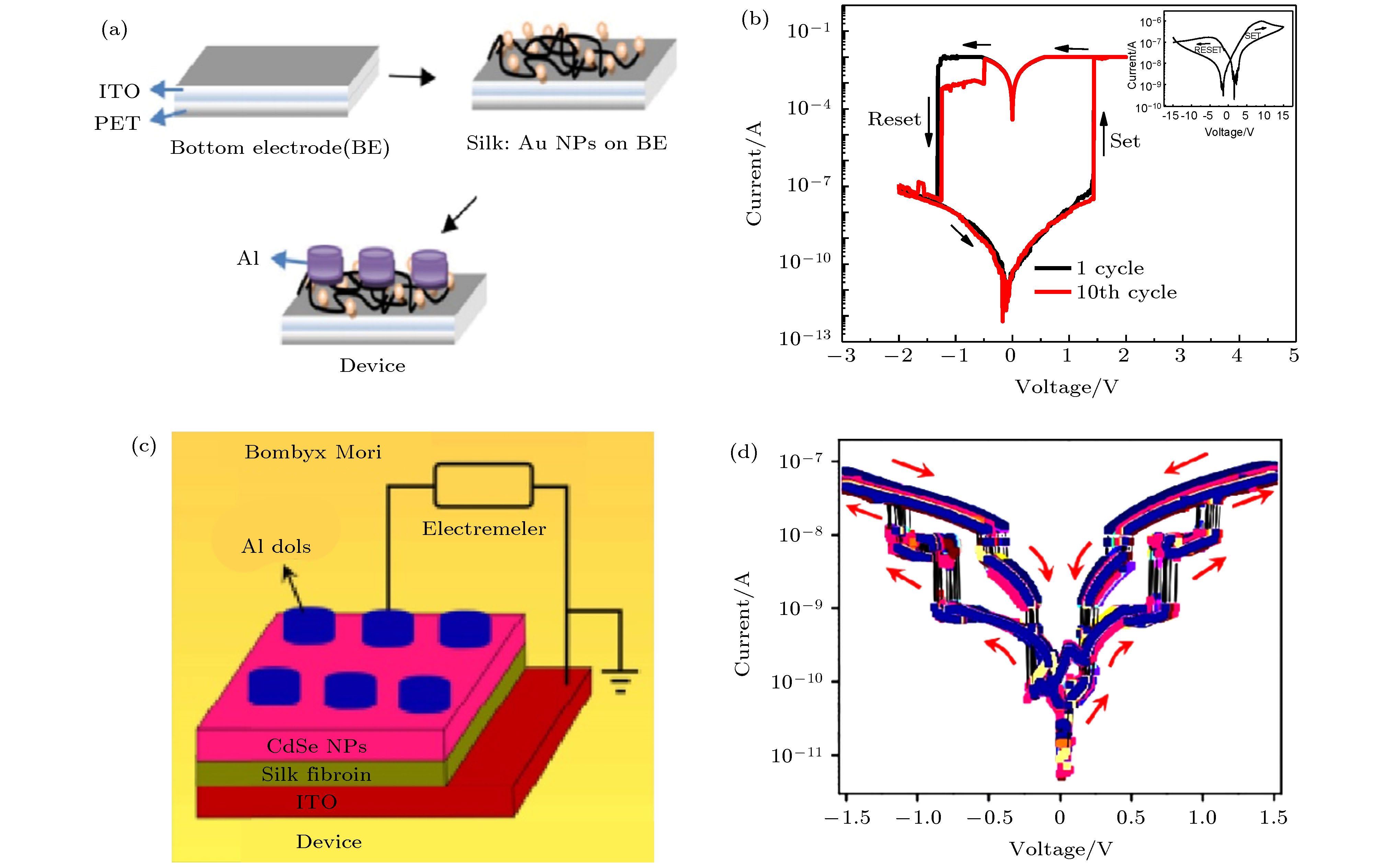
图 15 其他功能复合蚕丝蛋白基忆阻器 (a) 金颗粒掺杂蚕丝蛋白基忆阻器构建示意图; (b) 金颗粒掺杂蚕丝蛋白基忆阻器I-V性能曲线, 插图为纯蚕丝蛋白基忆阻器I-V特性曲线; (c) 硒化镉纳米颗粒负载蚕丝蛋白薄膜基忆阻器的器件结构示意图; (d) 器件的多级存储特性曲线[72,73]
Figure 15. Other functionalized silk fibroin based memristors: (a) Schema of Au nanoparticles functionalized silk memristor; (b) I-V switching characteristics of the ITO/silk fibroin-Au/Al device and the pure silk device (in the inset); (c) schema of CdSe-silk memristor; (d) multilevel memory switching of CdSe-silk memristor[72,73].
表 1 蛋白质基忆阻器性能比较
Table 1. The comparison of protein-based memristors.
器件结构 开关比 开关电压/V 保持时长/s 擦写速度/ns 循环次数 Al/蚕丝蛋白/ITO[61] 10 10.4/–11.5 — — — Ag/蚕丝蛋白/Au[63] 107 1.3—3.4/–1.3 4.5 × 10³ — — Ag/蚕丝蛋白/Au[64] 105 0.7—1.7/–1.2 104 — 30 Mg/蚕丝蛋白/Mg[65] 104 0.7—1.7/–1 104 — 50 Au/蚕丝蛋白/Pt[74] 104 3/–1.7 5.7 × 10³ — 30 Al/CdSe-蚕丝蛋白/ITO[73] — — 104 — — Ag/Au-蚕丝蛋白/ITO[68] 102 0.4/–0.2 1.4 × 10⁴ — 100 Ag/Ag-蚕丝蛋白/ITO[24] 103 0.3/–0.18 104 10 100 Al/CDs-蚕丝蛋白/ITO[70] — 3/–1 106 — 100 W/鸡蛋白蛋白/ITO[32] 102 2/7 — — 100 Ag/鸡蛋白蛋白/Al[75] 102 0.6/–0.7 104 75 50 Pt/铁蛋白/Pt[34] 105 2.2/–1.1 6 × 10³ — 70 Ag/丝胶蛋白/Au[33] 106 2.5/–0.8 103 — 21 Al/S-layer/ITO[35] 6.2 8/–8 4 × 10³ — 500 Cu/rDnaj/Pt[41] 106 0.12/–0.08 106 — 100 Ag/角蛋白/FTO[50] 103 1.5/–1.5 104 — 100 Ag/溶菌酶/Pt[47] 106 1/–1.3 104 100 200 -
[1] Borghetti J, Snider G S, Kuekes P J, Yang J J, Stewart D R, Williams R S 2010 Nature 464 873
 Google Scholar
[2] Strukov D B, Snider G S, Stewart D R, Williams R S 2008 Nature 453 80
 Google Scholar
[3] Wang M, Cai S, Pan C, Wang C, Lian X, Zhuo Y, Xu K, Cao T, Pan X, Wang B, Liang S J, Yang J J, Wang P, Miao F 2018 Nat. Electron. 1 130
 Google Scholar
[4] Zhou L, Mao J, Ren Y, Han S T, Roy V A L, Zhou Y 2018 Small 14 1703126
 Google Scholar
[5] Wang Z, Wang L, Nagai M, Xie L, Yi M, Huang W 2017 Adv. Electron. Mater. 3 1600510
 Google Scholar
[6] Yan X, Zhao J, Liu S, Zhou Z, Liu Q, Chen J, Liu X Y 2018 Adv. Funct. Mater. 28 1705320
 Google Scholar
[7] Yan X, Zhou Z, Zhao J, Liu Q, Wang H, Yuan G, Chen J 2018 Nano Research 11 1183
 Google Scholar
[8] Yan X, Wang J, Zhao M, Li X, Wang H, Zhang L, Lu C, Ren D 2018 Appl. Phys. Lett. 113 013503
 Google Scholar
[9] Yan X, Cao G, Wang J, Man M, Zhao J, Zhou Z, Wang H, Pei Y, Wang K, Gao C 2020 J. Mater. Chem. C 8 4926
 Google Scholar
[10] Lv Z, Zhou Y, Han S T, Roy V A L 2018 Mater. Today 21 537
 Google Scholar
[11] Pan F, Gao S, Chen C, Song C, Zeng F 2014 Mater. Sci. Eng. R 83 1
 Google Scholar
[12] Ji Y, Yang Y, Lee S K, Ruan G, Kim T W, Fei H, Lee S H, Kim D Y, Yoon J, Tour J M 2016 ACS Nano 10 7598
 Google Scholar
[13] Chang Y C, Wang Y H 2014 ACS Appl. Mater. Inter. 6 5413
 Google Scholar
[14] Goswami S, Matula A J, Rath S P, Hedstrom S, Saha S, Annamalai M, Sengupta D, Patra A, Ghosh S, Jani H, Sarkar S, Motapothula M R, Nijhuis C A, Martin J, Goswami S, Batista V S, Venkatesan T 2017 Nat. Mater. 16 1216
 Google Scholar
[15] Kim S, Jeong H Y, Kim S K, Choi S Y, Lee K J 2011 Nano Lett. 11 5438
 Google Scholar
[16] Lai Y C, Wang Y X, Huang Y C, Lin T Y, Hsieh Y P, Yang Y J, Chen Y F 2014 Adv. Funct. Mater. 24 1430
 Google Scholar
[17] Yan X, Zhao Q, Chen A P, Zhao J, Zhou Z, Wang J, Wang H, Zhang L, Li X, Xiao Z 2019 Small 15 1901423
 Google Scholar
[18] Yan X, Wang K, Zhao J, Zhou Z, Wang H, Wang J, Zhang L, Li X, Xiao Z, Zhao Q 2019 Small 15 1900107
 Google Scholar
[19] Zhou Z, Zhao J, Chen A P, Pei Y, Xiao Z, Wang G, Chen J, Fu G, Yan X 2020 Mater. Horiz. 7 1106
 Google Scholar
[20] Breivik K, Armitage J M, Wania F, Jones K C 2014 Environ. Sci. Technol. 48 8735
 Google Scholar
[21] Li Y, Xu X, Wu K, Chen G, Liu J, Chen S, Gu C, Zhang B, Zheng L, Zheng M, Huo X 2008 J. Environ. Monit. 10 1233
 Google Scholar
[22] Irimia Vladu M, Głowacki E D, Voss G, Bauer S, Sariciftci N S 2012 Mater. Today 15 340
 Google Scholar
[23] Zhou Z, Yan X, Zhao J, Lu C, Ren D, Lu N, Wang J, Zhang L, Li X, Wang H 2019 J. Mater. Chem. C 7 1561
 Google Scholar
[24] Shi C, Wang J, Sushko M L, Qiu W, Yan X, Liu X Y 2019 Adv. Funct. Mater. 29 1904777
 Google Scholar
[25] Zhu B, Wang H, Leow W R, Cai Y, Loh X J, Han M Y, Chen X 2016 Adv. Mater. 28 4250
 Google Scholar
[26] Zhou G, Ren Z, Wang L, Sun B, Duan S, Song Q 2019 Mater Horiz 6 1877
 Google Scholar
[27] Chen Y C, Yu H C, Huang C Y, Chung W L, Wu S L, Su Y K 2015 Sci. Rep. 5 10022
 Google Scholar
[28] Qiu W, Patil A, Hu F, Liu X Y 2019 Small 15 1903948
 Google Scholar
[29] He X, Zhang J, Wang W, Xuan W, Wang X, Zhang Q, Smith C G, Luo J 2016 ACS Appl. Mater. Inter 8 10954
 Google Scholar
[30] Sun B, Zhang X, Zhou G, Li P, Zhang Y, Wang H, Xia Y, Zhao Y 2017 Org. Electron. 42 181
 Google Scholar
[31] Kim S U, Yagati A K, Min J, Choi J W 2010 Biomaterials 31 1293
 Google Scholar
[32] Yan X, Li X, Zhou Z, Zhao J, Wang H, Wang J, Zhang L, Ren D, Zhang X, Chen J, Lu C, Zhou P, Liu Q 2019 ACS Appl. Mater. Inter 11 18654
 Google Scholar
[33] Wang H, Meng F, Cai Y, Zheng L, Li Y, Liu Y, Jiang Y, Wang X, Chen X 2013 Adv. Mater. 25 5498
 Google Scholar
[34] Zhang C, Shang J, Xue W, Tan H, Pan L, Yang X, Guo S, Hao J, Liu G, Li R W 2016 Chem. Commun. 52 4828
 Google Scholar
[35] Moudgil A, Kalyani N, Sinsinbar G, Das S, Mishra P 2018 ACS Appl. Mater. Inter 10 4866
 Google Scholar
[36] Sun B, Liang D, Li X, Chen P 2015 J. Mater. Sci. Mater. Electron. 27 3957
[37] Poul Nissen J H, Nenad Ban, Peter B. Moore, Thomas A. Steitz 2000 Science 289 920
 Google Scholar
[38] Johnson E, Cascio D, Sawaya M R, Gingery M, Schröder I 2005 Structure 13 637
 Google Scholar
[39] Meng F, Sana B, Li Y, Liu Y, Lim S, Chen X 2014 Small 10 277
 Google Scholar
[40] Yongmin Ko Y K, Hyunhee Baek, and Jinhan Cho 2011 ACS Nano 5 9918
 Google Scholar
[41] Jang S K, Kim S, Salman M S, Jang J R, Um Y M, Tan L, Park J H, Choe W S, Lee S 2018 Chem. Mater. 30 781
 Google Scholar
[42] Debabov V G 2004 Mol. Biol. 38 578
[43] Khaleghi M, Kermanshahi R K, Yaghoobi M, Zarkesh Esfahani S, Baghizadeh A 2010 J. Microbiol. Biotechnol. 20 749
[44] Howorka S, Sára M, Wang Y, Kuen B, Sleytr U B, Lubitz W, Bayley H 2000 J. Biol. Chem. 275 37876
 Google Scholar
[45] Iturri J, Vianna A C, Moreno Cencerrado A, Pum D, Sleytr U B, Toca Herrera J L 2017 Beilstein J. Nanotechnol. 8 91
 Google Scholar
[46] Sára M, Sleytr U B 2000 J. Bacteriol. 182 859
 Google Scholar
[47] Baek H, Lee C, Lim K I, Cho J 2012 Nanotechnology 23 155604
 Google Scholar
[48] Ko J, Nguyen L T H, Surendran A, Tan B Y, Ng K W, Leong W L 2017 ACS Appl. Mater. Inter 9 43004
 Google Scholar
[49] Singh R, Lin Y T, Chuang W L, Ko F H 2017 Org. Electron. 44 198
 Google Scholar
[50] Lin Q, Hao S, Hu W, Wang M, Zang Z, Zhu L, Du J, Tang X 2019 J. Mater. Chem.C 7 3315
 Google Scholar
[51] Idris A, Vijayaraghavan R, Rana U A, Patti A F, MacFarlane D R 2014 Green Chem. 16 2857
 Google Scholar
[52] Bhushan B 2008 Prog. Mater. Sci. 53 585
 Google Scholar
[53] Reddy N, Hu C, Yan K, Yang Y 2011 Mater. Sci. Eng. C 31 1706
 Google Scholar
[54] Rouse J G, Van Dyke M E 2010 Materials 3 999
 Google Scholar
[55] Guo B, Sun B, Hou W, Chen Y, Zhu S, Mao S, Zheng L, Lei M, Li B, Fu G 2019 Rsc Adv. 9 12436
 Google Scholar
[56] Tu H, Yu R, Lin Z, Zhang L, Lin N, Yu W D, Liu X Y 2016 Adv. Funct. Mater. 26 9032
 Google Scholar
[57] Lin N, Cao L, Huang Q, Wang C, Wang Y, Zhou J, Liu X Y 2016 Adv. Funct. Mater. 26 8885
 Google Scholar
[58] Chen Z, Zhang H, Lin Z, Lin Y, van Esch J H, Liu X Y 2016 Adv. Funct. Mater. 26 8978
 Google Scholar
[59] Song Y, Lin Z, Kong L, Xing Y, Lin N, Zhang Z, Chen B H, Liu X Y 2017 Adv. Funct. Mater. 27 1700628
 Google Scholar
[60] Shi C, Xing Y, Patil A, Meng Z, Yu R, Lin N, Qiu W, Hu F, Liu X Y 2019 ACS Appl. Mater. Inter. 11 30125
 Google Scholar
[61] Hota M K, Bera M K, Kundu B, Kundu S C, Maiti C K 2012 Adv. Funct. Mater. 22 4493
 Google Scholar
[62] Mukherjee C, Hota M K, Naskar D, Kundu S C, Maiti C K 2013 Phys. Status Solidi A 210 1797
 Google Scholar
[63] Wang H, Du Y, Li Y, Zhu B, Leow W R, Li Y, Pan J, Wu T, Chen X 2015 Adv. Funct. Mater. 25 3825
 Google Scholar
[64] Wang H, Zhu B, Wang H, Ma X, Hao Y, Chen X 2016 Small 12 3360
 Google Scholar
[65] Wang H, Zhu B, Ma X, Hao Y, Chen X 2016 Small 12 2715
 Google Scholar
[66] Kook G, Jeong S, Kim M K, Lee S, Choi N, Lee H J 2020 Adv. Mater. Technol. 5 1900991
 Google Scholar
[67] Lin N, Liu X Y 2015 Chem. Soc. Rev. 44 7881
 Google Scholar
[68] Xing Y, Shi C, Zhao J, Qiu W, Lin N, Wang J, Yan X B, Yu W D, Liu X Y 2017 Small 13 1702390
 Google Scholar
[69] Lv Z, Wang Y, Chen J, Wang J, Zhou Y, Han S T 2020 Chem. Rev. 120 3941
 Google Scholar
[70] Lv Z, Wang Y, Chen Z, Sun L, Wang J, Chen M, Xu Z, Liao Q, Zhou L, Chen X, Li J, Zhou K, Zhou Y, Zeng Y J, Han S T, Roy V A L 2018 Adv. Sci. 5 1800714
 Google Scholar
[71] Lv Z, Chen M, Qian F, Roy V A L, Ye W, She D, Wang Y, Xu Z X, Zhou Y, Han S T 2019 Adv. Funct. Mater. 29 1902374
 Google Scholar
[72] Gogurla N, Mondal S P, Sinha A K, Katiyar A K, Banerjee W, Kundu S C, Ray S K 2013 Nanotechnology 24 345202
 Google Scholar
[73] Murgunde B K, Rabinal M K 2017 Org. Electron. 48 276
 Google Scholar
[74] Yong J, Hassan B, Liang Y, Ganesan K, Rajasekharan R, Evans R, Egan G, Kavehei O, Li J, Chana G, Nasr B, Skafidas E 2017 Sci. Rep. 7 14731
 Google Scholar
[75] Zhu J X, Zhou W L, Wang Z Q, Xu H Y, Lin Y, Liu W Z, Ma J G, Liu Y C 2017 Rsc Adv. 7 32114
 Google Scholar
[76] Yan X, Pei Y, Chen H, Zhao J, Zhou Z, Wang H, Zhang L, Wang J, Li X, Qin C 2019 Adv. Mater. 31 1805284
 Google Scholar
[77] Yan X, Zhang L, Chen H, Li X, Wang J, Liu Q, Lu C, Chen J, Wu H, Zhou P 2018 Adv. Funct. Mater. 28 1803728
 Google Scholar
[78] Yang J J, Strukov D B, Stewart D R 2013 Nat. Nanotechnol. 8 13
 Google Scholar
Catalog
Metrics
- Abstract views: 17345
- PDF Downloads: 437
- Cited By: 0


 DownLoad:
