


SPECIAL TOPIC—Flexible electronics

2020, 69 (17): 170202.
doi: 10.7498/aps.69.20200867
Abstract +
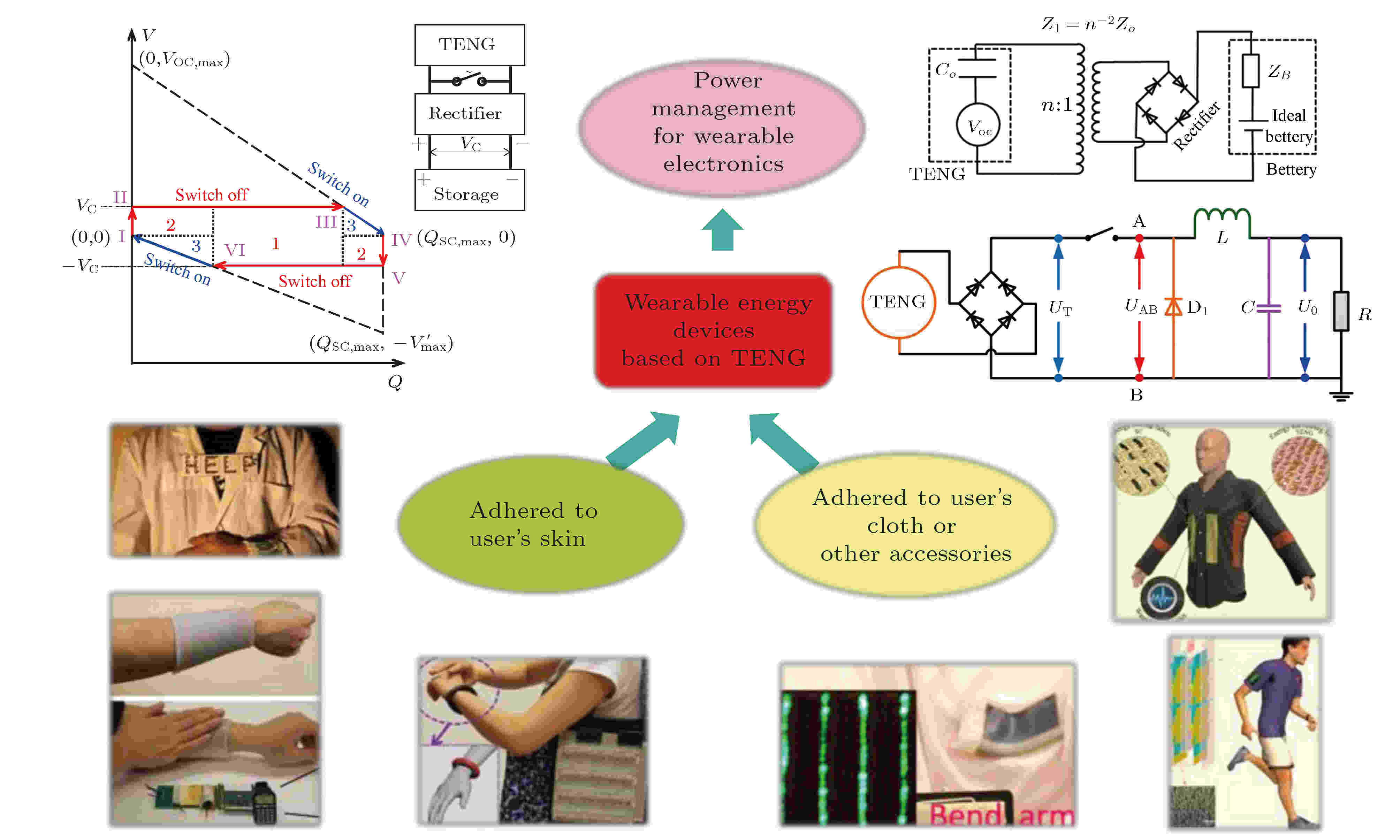
With the miniaturization and functionalization of electronic devices, wearable electronics has drawn generally attention, but the energy supply for wearable electronics becomes one of the most burning questions. The triboelectric nanogenerator based on the coupling effects of electrostatic induction and triboelectrification, which has low cost and wide material selection attributes, proves to be a powerful technology for converting low-frequency mechanical energy into electricity. In this review, the four fundamental modes of triboelectric nanogenerator and the physical mechanism of contact-electrification are presented first. Then, we introduce the research progress of wearable from the direct and indirect aspects. Directly wearable triboelectric nanogenerator can be integrated into a skin while indirectly wearable device is only allowed to assemble into user’s clothing or its appendages. In addition, the power management circuits for driving electronic devices and energy storage are summarized. Finally, we discuss the current bottlenecks and present our perspectives on future directions in this field.

2020, 69 (17): 170701.
doi: 10.7498/aps.69.20200784
Abstract +
Low-cost, easy-to-deploy and self-driven flexible electronic devices and flexible sensors will bring new opportunities for developing the internet of things, wearable, and implantable technologies, especially human health monitoring, tactile perception and intelligent robot electronic skin. Therefore, it is necessary to provide high-performance and continuous energy supply modules for flexible electronic devices and flexible sensors. Nanogenerator can achieve high-performance sensing and energy storage characteristics by regulating the polarization electric field at the interface and surface, which is indeed an ideal adaptation choice. In particular, flexible piezoelectric nanogenerator can convert mechanical energy into electrical energy by piezoelectric properties, and can be applied to various deformation conditions such as bending, stretching and compression, which provides a novel solution to the problems of limited energy supply and insufficient performance in flexible electronic and self-driven technology. The piezoelectric output response of piezoelectric nanogenerator can be used not only as an energy signal to self-drive flexible electronic devices, but also as a sensing signal that can be integrated into the self-driven flexible sensors such as gas sensor, pressure sensor and biological sensor. Predictably, self-powered gas sensor with energy harvesting and high-sensitivity sensing, and self-charging power cell with energy harvesting and efficient storage will become hot topics. In this paper, we review the recent developments of flexible piezoelectric nanogenerators in flexible sensors and energy storage devices.

2020, 69 (17): 177401.
doi: 10.7498/aps.69.20200632
Abstract +
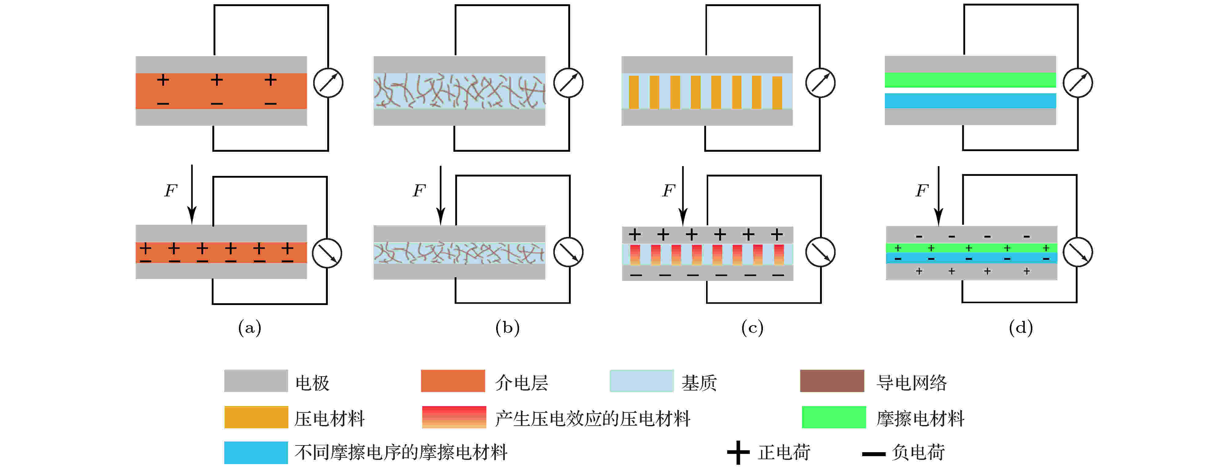
Flexible stretchable conductors have attracted wide attention due to their promising applications in information, energy, medical, national defense and other fields, where elastic conductors undergo large deformation and form intimate contact with three-dimensional irregular surfaces. Many conductive nanomaterials with excellent properties have been developed over the past decades, such as metal nanowires, carbon nanotubes, graphene and conductive polymers. One efficient method to prepare stretchable conductor is to disperse conductive materials into elastic matrix to form a conductive network, showing stretchability and conductivity. As an alternative way, elastic conductors show stable resistance change during stretch by use of buckled or serpentine structural design for rigid conductors. This review summarizes recent advances in flexible elastic conductors in the past five years. In addition, some flexible electronic devices such as light-emitting diodes, sensors, heaters, etc. are also discussed and the development direction in the field of flexible electronic devices is also suggested.
2020, 69 (17): 178102.
doi: 10.7498/aps.69.20200987
Abstract +
As an emerging type of electronic devices, flexible pressure sensors have more advantages than rigid sensors in human-computer interaction, healthcare, and tactile sensing in robots. These advantages, however, require the materials to be thin and soft. For applications in human bodies, the sensor needs to be biocompatible and mechanically match the biotissue such that they can be conformable to the skin textures, or be implanted in the body. Sensitivity, response time, limitation of detection, and stability are basic properties to evaluate a pressure sensor. Recently, some other parameters of flexible pressure sensors including pressure response range, pressure resolution, space resolution, and stretchability have also been studied, enabling such devices to have a wider application prospect. This review introduces about the state of the arts of flexible pressure sensors in recent years, and is intended to discuss the sensing mechanisms, properties, and potential applications of flexible tactile sensors. At last, we talk about the future of flexible tactile sensors.

2020, 69 (17): 178201.
doi: 10.7498/aps.69.20200159
Abstract +
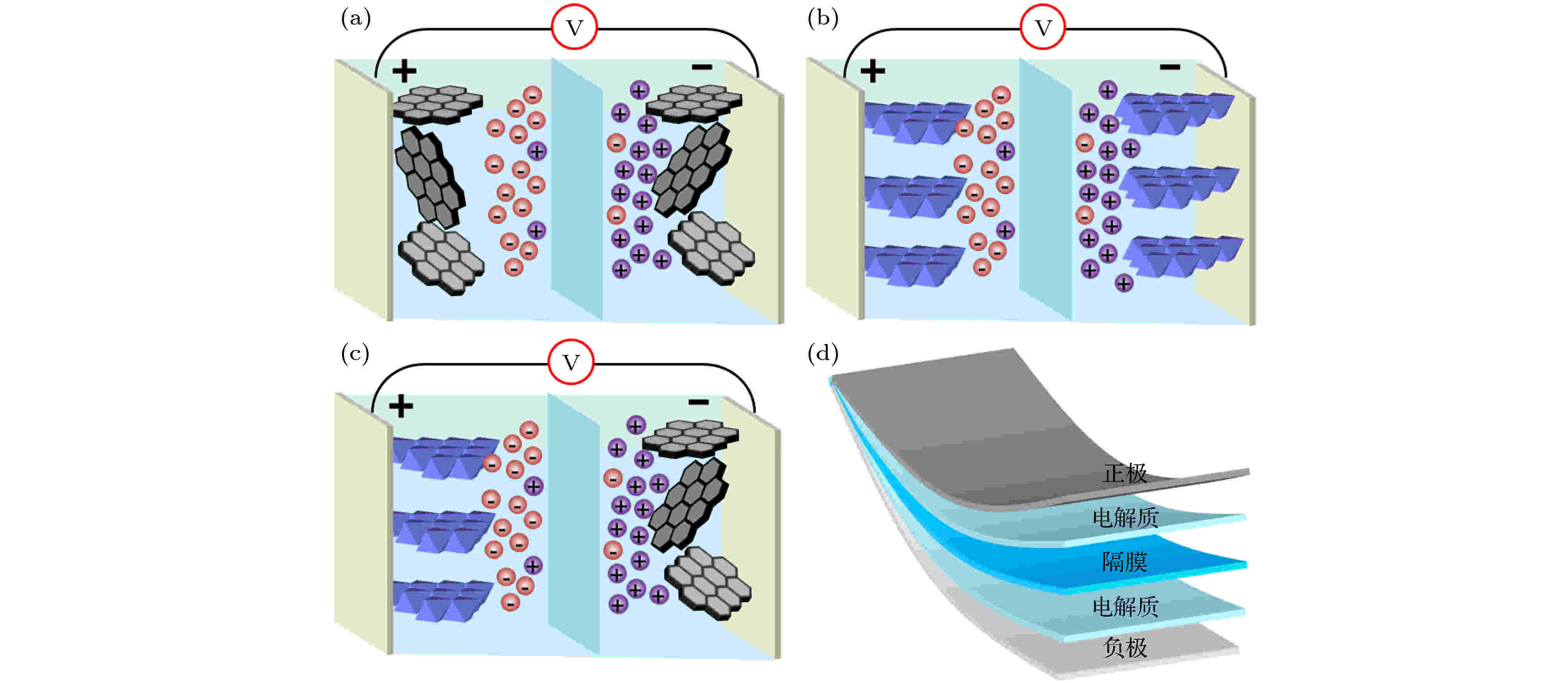
With the continuous development of today's flexible electronic products, fiber-shaped supercapacitors (fiber-shaped supercapacitors, FSCs) have attracted continuous attention. That’s due to their advantages such as light weight, controllable volume, good bending and tensile properties, and weavable. Fiber-shaped supercapacitors, with their unique one-dimensional fiber structure, can be combined with various other electrical or power generation devices into multifunctional integrated fiber-shaped electronic devices, which have huge application prospects in the field of wearable electronic textiles. This article describes the latest developments in fiber-shaped supercapacitor devices. Firstly, different fiber substrates are introduced and their advantages and disadvantages are analyzed as well. It also summarizes the electrode materials such as carbon materials, metal oxides and sulfides, conductive polymers, and hybrid nanocomposites of fiber-shaped supercapacitors. By analyzing the differences and characteristics of different electrode materials, it is shown that different electrode materials are suitable for different uses in fiber-shaped supercapacitors. Then we also summarize the application of fiber-shaped supercapacitors in cooperation with other devices to form integrated devices, including integration with general power devices, sensors, other photoelectric conversion devices and other power generation devices into hybrid devices and applied to practice. Finally, by summarizing the recent development results of fiber-shaped supercapacitors and the current challenges in the field, some current bottlenecks and problems of fiber-shaped supercapacitors are proposed, and some suggestions and ideas for the future development direction are put forward.
2020, 69 (17): 178701.
doi: 10.7498/aps.69.20200664
Abstract +
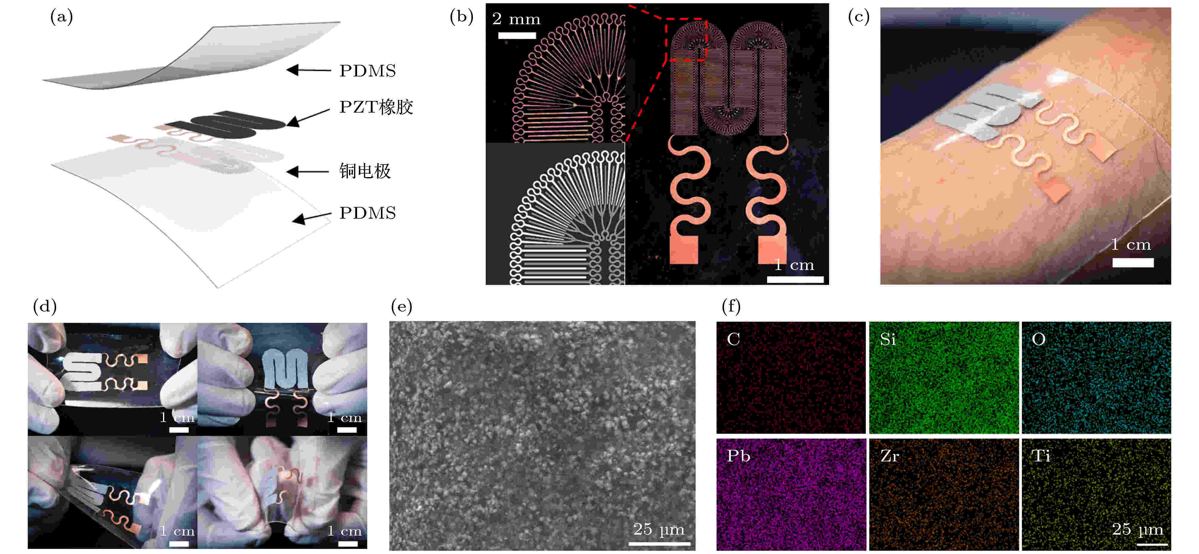
Soft, thin, skin-integrated electronics, i.e. epidermal electronics, has become a hotspot in biomedical engineering and drawn great attention for their applications in health monitoring, disease diagnosis and therapies. However, soft powering system is still a challenge for epidermal electronics, since the thickness and weight of the existing flexible energy harvesting and storage devices are very hard to meet the requirements of epidermal electronics. Here we present a stretchable and flexible self-powering epidermal electronic device based on rubbery piezoelectric composites formed by a ternary blend of PDMS, lead zirconate titanate (PZT) and graphene. The mixed PZT rubber is soft, ultra-thin and light weight and intrinsically stretchable. By combining soft PDMS substrate and advanced mechanics designed interdigital electrodes/interconnects, a stretchable and skin-integrated device for tactile sensing is realized. The soft device can not only accurately measure a board range of force from 2.84 kPa to 11.72 kPa but also exhibit great flexibility that can maintain stable performance under various mechanical deformations, such as bending, stretching and twisting. On-skin demonstration tests reveal that this self-powering device can clearly distinguish the differences among mechanical stimulations such as touching, poking, tapping and hitting. Furthermore, the self-powering nature of these devices allows energy to be harvested from daily body actives, for instance, hard touching by hand can lighten up to 15 light-emitting diodes.

2020, 69 (17): 178702.
doi: 10.7498/aps.69.20200617
Abstract +
Memristor, as a new type of electronic component that can realize high density, multi-function, low power consumption, and multi-level data storage, has brought significant changes to the field of circuit structure design, information storage theory, and artificial synapses simulation. In a wide range of memristors, the protein-based memristors have unparalleled natural advantages in other cutting-edge information technology fields such as implantable computing, human-computer interaction, and human-computer integration due to their controllable degradation, rich and cheap raw materials, and biocompatibility. Therefore, the memristor is considered as the most potential candidate for building the next generation of high-tech information electronic device. In this article, the latest research progress of protein based memristors is comprehensively reviewed. The research progress of other proteins, including the widely studied egg albumen and artificial recombinant protein with excellent performance are first summarized, and then the research process of silk fibroin-based memristors, the performance improvement of silk fibroin-based memristors brought by functional strategies are comprehensively introduced. The Structure-activity relationship between structure and performance of functionalized silk fibroin is analyzed. Finally, the performance of the protein-based memristor is comprehensively analyzed, and the future development opportunities of the green electronic device are also prospected.

2020, 69 (17): 178703.
doi: 10.7498/aps.69.20200818
Abstract +
In recent years, wearable electronics has received extensive attention, providing new opportunities for implementing health monitoring, human disease diagnosis and treatment, and intelligent robotics. Sensor is one of the key components of wearable electronics. Silk (Bombyx Mori) material shows unique features including high yield, excellent tensile strength (0.5–1.3 GPa) and toughness ((6–16) × 104 J/kg), good biocompatibility, programmable/controllable biodegradability, novel dielectric properties, and various material formats. With the rapid development of biomaterials and related manufacturing technologies, advanced silk-based materials have been studied and applied to wearable sensors. Here, we firstly introduce the five-level structure of silk fibroin from bottom to top and characteristics of silk-based advanced materials, and then review the research progress of silk-based advanced materials in wearable sensors in recent years, including mechanical sensors, electrophysiological sensors, temperature sensors and humidity sensors. The working mechanism, structure and performance of different sensors, the role of silk proteins in them, and their applications in health monitoring are discussed and summarized. Finally, the challenges and future prospects of silk-based wearable sensors in practical applications are put forward.
2020, 69 (17): 178704.
doi: 10.7498/aps.69.20201012
Abstract +
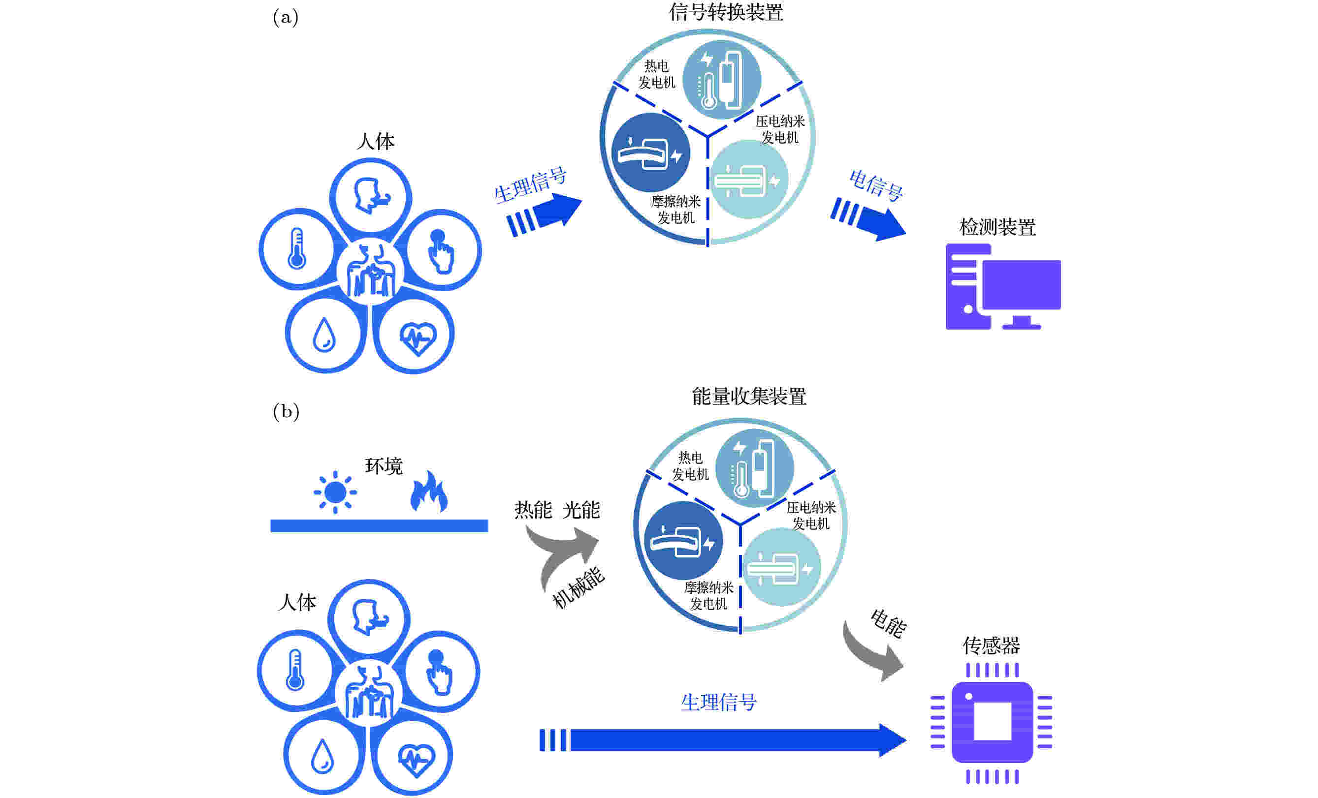
In recent years, flexible biomedical sensors have received extensive attention and achieved great development. However, the battery life of flexible biomedical sensors is limited, which has become a bottleneck restricting the development of flexible biomedical sensors. The concept of self-powered flexible biomedical sensor provides an important idea for solving battery life problem. This review summarizes the research progress of self-powered flexible biomedical sensors over the years. Besides, this review discusses several self-powered flexible biomedical sensors based on different power generation technologies and different materials, as well as their respective advantages and scope of application. Further, some representative research works are selected and discussed in detail. Self-powered flexible biomedical sensors can be divided into wearable self-powered flexible biomedical sensors and implantable self-powered flexible biomedical sensors according to their working positions, which can be used to collect important physiological indicators such as human respiration, pulse, temperature, etc. Finally, this paper also predicts and evaluates the future research direction of self-powered flexible biomedical sensors.
EDITOR'S SUGGESTION
2020, 69 (17): 178801.
doi: 10.7498/aps.69.20200881
Abstract +
Stretchable supercapacitors have received more and more attention due to their potential applications in wearable electronics and health monitoring. The stretchable supercapacitors have not only the advantages of high power density, long cycle life, safety and low cost of ordinary supercapacitor, but also good flexibility and stretchability to integrate well with wearable system. In this review, according to the structures of supercapacitors, the methods of preparing stretchable electrodes/devices reported in the literature are categorized and analyzed. We particularly highlight the key findings of creating stretchable electrodes/devices, which include elastic polymer substrates, tensile structure design and elastic polymer + tensile structure. In addition, the research progress of multi-functional stretchable supercapacitors and high elastic gel electrolytes are discussed. Finally, the challenges to the future development of the stretchable supercapacitors are analyzed and summarized. We expect to stimulate more research in creating stretchable supercapacitors for wide practical applications.
REVIEW
EDITOR'S SUGGESTION
2020, 69 (17): 177801.
doi: 10.7498/aps.69.20200724
Abstract +
An important feature of the irradiation process in nuclear system is the formation of large displacement cascades, in which primary knock-on atoms and secondary particles formed by nuclear reactions generate a considerable number of defects such as dislocations, vacancies and transmutation gases. Predicting and mitigating the adverse effects of damage defect and transmutation hydrogen/helium produced by high-dose neutron irradiation on the mechanical properties of structural materials is the most significant challenge facing the current development of nuclear energy. To solve this problem, understanding the interaction mechanism between hydrogen/helium atoms and micro-defects is a very important breakthrough. Precursors of helium/ hydrogen bubble, small helium/hydrogen-filled vacancy complexes, may play an important role in realizing bubble nucleation, and the formation of these complexes is affected by many factors. However, only a little information about helium/hydrogen-vacancy clusters’ behavior has been obtained in metal/alloy materials. This is mainly limited by the characterization methods, such as the limited resolution of transmission electron microscope (TEM). Helium/hydrogen-vacancy clusters cannot be observed by TEM before the formation of helium bubbles. Applications of positron annihilation to the study of crystal lattice defects started around 1970s, when it was realized that positron annihilation is particularly sensitive to vacancy-type defects and that annihilation properties manifest the nature of each specific type of defect. In recent years, with the continuous development of slow positron beam and the improvement of various experimental testing methods based on slow positron beam, the application of positron annihilation technology has been extended to the research field of hydrogen/helium behavior in metal materials, which plays an important role in studying the hydrogen/helium radiation damage to metal materials. In this review, the basic principles of positron annihilation spectroscopy are briefly discussed and the three most important measurement methods used for hydrogen/helium effect studies are described (i.e. positron annihilation lifetime spectroscopy (PALS), Doppler broadening spectroscopy (DBS), coincidence Doppler broadening spectroscopy (CDBS)). In this paper, the application of positron annihilation spectroscopy to the study of hydrogen/helium behavior in metal materials is reviewed in combination with the reported relevant developments (including our research group’s achieve-ments). The advantages of three commonly used measurement methods in the following specific studies are highlighted: 1) The estimation of bubble size and concentration; 2) irradiation damage induced by hydrogen/helium; 3) the evolution behavior of irradiation-induced defects in the heat treatment process; 4) sy-nergistic effect of hydrogen and helium.
EDITOR'S SUGGESTION
2020, 69 (17): 177101.
doi: 10.7498/aps.69.20200656
Abstract +
Defect control of semiconductors is critical to the photoelectric conversion efficiency of solar cells, because the defect and doping directly determine the carrier distribution, concentration, charge transfer and non-radiative recombination of photogenerated carriers. The defect types, structures and properties are complicated in the real semiconductors, which makes experimental characterization difficult, especially for the point defects. In this review, we firstly introduce the approaches of defect calculation based on the first-principles calculations, and take a series of typical solar cell materials for example, including CdTe, Cu(In/Ga)Se2, Cu2ZnSnS(Se)4 and CH3NH3PbI3. The elucidating of computations is also conducible to understanding and controlling the defect properties of solar cell materials in practical ways. The comparative study of these solar cell materials indicates that their efficiency bottlenecks are closely related to their defect properties. Unlike the traditional four-coordination semiconductor, the unique “defect tolerance” characteristic shown in the six-coordination perovskite materials enables the battery to have a high photoelectric conversion efficiency even when it is prepared not under harsh experimental conditions. Based on the first principles, the defect calculation plays an increasingly important role in understanding the material properties of solar cells and the bottleneck of device efficiency. At present, the calculation of defects based on the first principle mainly focuses on the formation energy and transition energy levels of defects. However, there is still a lack of researches on the dynamic behavior of carriers, especially on the non-radiative recombination of carriers, which directly affects the photoelectric conversion efficiency. Recently, with the improvement of computing power and the development of algorithms, it is possible to quantitatively calculate the electron-ion interaction, then quantitatively calculate the carriers captured by defect state. These methods have been used to study the defects of solar cells, especially perovskite solar cells. In this direction, how to combine these theoretical calculation results with experimental results to provide a more in-depth understanding of experimental results and further guide experiments in improving the efficiency of solar cells is worthy of further in-depth research.
GENERAL

2020, 69 (17): 170201.
doi: 10.7498/aps.69.20191920
Abstract +
Kalman filter time scale algorithm is a method of real-time estimating atomic clock state. It is of great practical value in the time-keeping work. Reliable Kalman filter time scale algorithm requires a reliable atomic clock state model, a random model and a reasonable estimation method. However, it is difficult to construct accurate state model when the noises of atomic clock change. The random model is generally based on the prior statistical information about atomic clock noises, and the prior statistical information may be distorted. In the process of time scale calculation, the noises of atomic clocks need estimating in the Kalman filter time scale algorithm, which is quantified according to the intensity of the noise. With the change of the external environment or aging of atomic clock, the noise intensity may change, resulting in the disturbance of atomic clock state estimation in the Kalman filter time scale algorithm, which further affects the accuracy and stability of the time scale. On the other hand, the error of the noise intensity estimation of atomic clocks will also affect the performance of time scale. Therefore, it is necessary to control the disturbance caused by the variation of noise intensity or the estimation error of noise intensity. In this regard, an adaptive factor is introduced to improve the Kalman filter time scale algorithm, and another adaptive factor is introduced into the state prediction covariance matrix in Kalman filter time scale algorithm. And the values of the two adaptive factors are calculated in real time by using statistics to control the growth of the state prediction covariance. The disturbance of state estimation of atomic clock is reduced, and the accuracy and stability of time scale are improved. In this paper, the sampling interval of simulated data and the measured data are 300 s and 3600 s respectively. The simulated data and measured data are used to calculate the overlapping Allan deviations of the time scale. The results show that the improved Kalman filter time scale algorithm can improve the stability of the sampling time more than 14400 s compared with classical Kalman filter time scale algorithm, and affect the stability of the sampling time less than 14400 s. The degree of influence is related to the weight algorithm of atomic clock. The measured data in this paper are treated by the “predictability” weighting algorithm, which guarantees the long-term stability of time scale. So the simulated data and measured data show that compared with classical Kalman filter time scale algorithm, the improved Kalman filter clock time scale algorithm can improve the accuracy and the long-term stability of time scale.

EDITOR'S SUGGESTION
2020, 69 (17): 170501.
doi: 10.7498/aps.69.20200394
Abstract +
The study of synchronizations in coupled oscillators is very important for understanding the occurrence of self-organized behaviors in complex systems. In the traditional Kuramoto model that has been extensively applied to the study of synchronous dynamics of coupled oscillators, the interaction function among oscillators is pairwise. The multiplex interaction mechanism that describes triple or multiple coupling functions has been a research focus in recent years. When the multiplex coupling dominates the interactions among oscillators, the phase oscillator systems can exhibit the typical abrupt desynchronization transitions. In this paper, we extensively investigate the synchronous dynamics of the Kuramoto model with mean-field triple couplings. We find that the abrupt desynchronization transition is irreversible, i.e. the system may experience a discontinuous transition from coherent state to incoherent state as the coupling strength deceases adiabatically, while the reversed transition cannot occur by adiabatically increasing the coupling. Moreover, the coherent state strongly depends on initial conditions. The dynamical mechanism of this irreversibility is theoretically studied by using the self-consistency approach. The neutral stability of ordered state is also explained through analyzing the linear-stability of the incoherent state. Further studies indicate that the system may experience a cascade of desynchronized standing-wave transitions when the width of the distribution function of natural frequencies of oscillators is changed. At the critical coupling, the motion of coupled oscillators in high-dimensional phase space becomes unstable through the saddle-node bifurcation and collapses into a stable low-dimensional invariant torus, which corresponds to the standing-wave state. The above conclusions and analyses are further extended to the case of multi-peak natural-frequency distributions. The results in this work reveal various collective synchronous states and the mechanism of the transitions among these macroscopic states brought by multiplex coupling. This also conduces to the in-depth understanding of transitions among collective states in other complex systems.
COVER ARTICLE
2020, 69 (17): 172901.
doi: 10.7498/aps.69.20200718
Abstract +
The back-streaming neutron beam line (Back-n) was built in the beginning of 2018, which is part of the China Spallation Neutron Source (CSNS). The Back-n is the first white neutron beam line in China, and its main application is for nuclear data measurement. For most of neutron-induced nuclear reaction measurements based on white neutron facilities, the beam of gamma rays accompanied with neutron beam is one of the most important experimental backgrounds. The back streaming neutron beam is transported directly from the spallation target to the experimental station without any moderator or shielding, the flux of the in-beam gamma rays in the experimental station is much larger than those of these facilities with neutron moderator and shielding. Therefore, it is necessary to consider the influence of in-beam gamma rays on the experimental results. Studies of the in-beam gamma rays are carried out at the back-n. Monte-Carlo simulation is employed to obtain the energy distribution and the time structure of the in-beam gamma rays. According to the simulation results, when the neutron flight time is longer than 1.0 μs the energy distribution of the in-beam gamma rays does not vary with flight time. Therefore, the time structure of these gamma rays can be measured without the correction of the detection efficiency. In this work, the time structure of the in-beam gamma rays in the low neutron energy region is measured by both direct and indirect methods. In the direct measurement, a 6Li loaded ZnS(Ag) scintillator is located on the neutron beam line and the time of flight method is used to determine the time structure of neutrons and gamma rays. The gamma rays are separated from neutrons with pulse-shape discrimination. The black filter method is used to verify the particle discrimination results. In the indirect measurement, the C6D6 scintillation detectors are used to measure the gamma rays scattered off a Pb sample on the way of the neutron beam. The time structure of the in-beam gamma rays is derived from that of the scattered gamma rays. The experimental results are in good agreement with the simulations with the time-of-flight between 12 μs and 2.0 ms. Besides, according to the simulation results, the intensity of the in-beam gamma rays is 1.21 × 10⁶ s–1·cm–2 in the center of the experimental station 2 of Back-n, which is 76.5 m away from the spallation target of CSNS.
ATOMIC AND MOLECULAR PHYSICS

2020, 69 (17): 173401.
doi: 10.7498/aps.69.20200218
Abstract +
Terahertz-streaking photoionization can be exploited to resolve ultrafast quantum beating and reconstruct the ultrafast evolution of density matrix. Here, we propose an experimental strategy to implement the method merely with the tabletop femtosecond system and magneto-optical trap reaction microscopy. The probe pulse consists of an ultraviolet pulse with pulse duration of about 30 fs and a strong terahertz pulse with strength of about 2.6 fs in rubidium-atom superposition. The population and coherence terms of the density matrix can be projected into different positions of the photoelectron momentum distribution. The reconstruction algorithm was designed to acquire the ultrafast evolution of density matrix from the time-dependent photoelectron spectrum. The experimental conception can demonstrate the newly proposed transient spectral method only with the commercial femtosecond laser system and magneto-optical trap reaction microscopy, thus preventing the complex laser system, such as extreme ultraviolet free electron lasers and attosecond higher harmonics, allowing a new metrology to explore the coherence dynamics of quantum systems.
ELECTROMAGNETISM, OPTICS, ACOUSTICS, HEAT TRANSFER, CLASSICAL MECHANICS, AND FLUID DYNAMICS
2020, 69 (17): 174201.
doi: 10.7498/aps.69.20200200
Abstract +


2020, 69 (17): 174202.
doi: 10.7498/aps.69.20200224
Abstract +
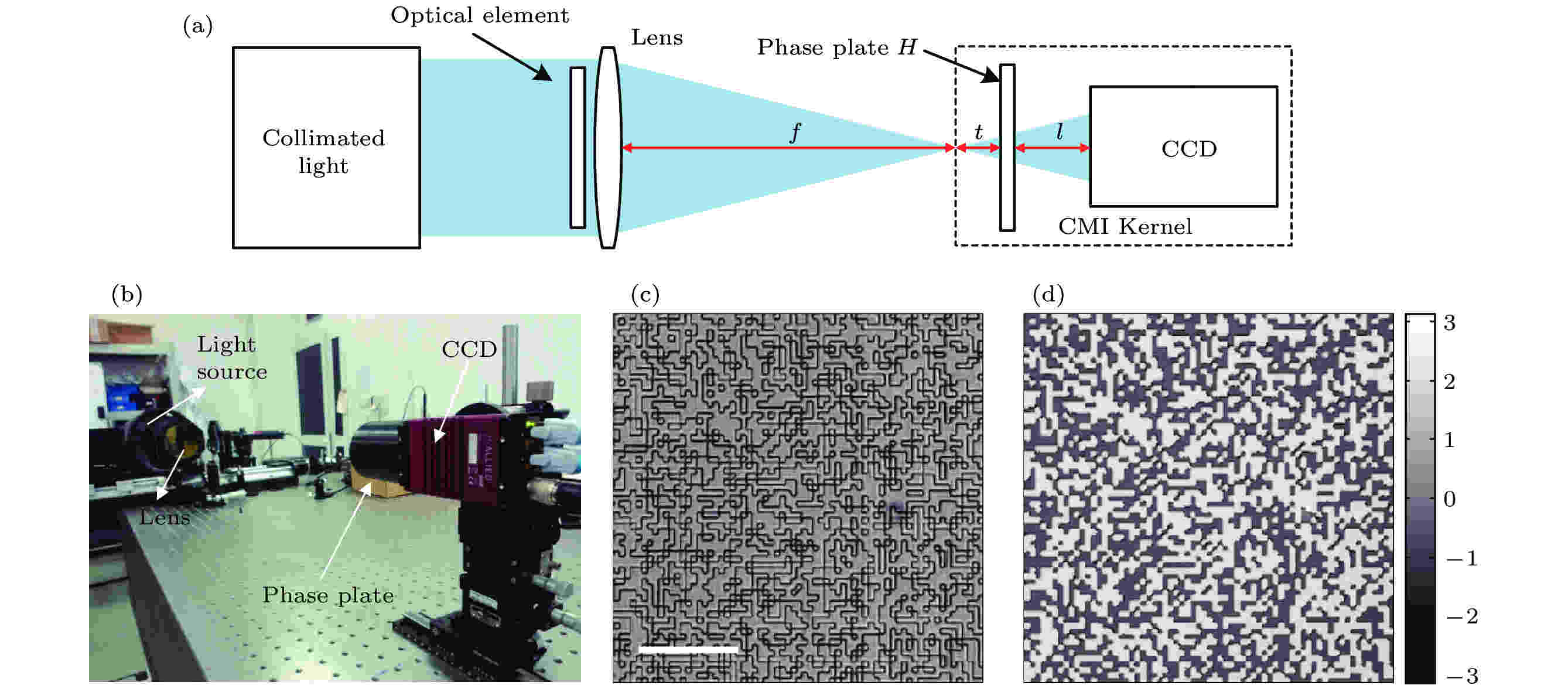
As one of the coherent diffractive imaging (CDI) techniques, coherent modulation imaging (CMI) is a lensless phase imaging technology with diffraction limited resolution in theory. Unlike multiple measurement phase retrieval algorithms, the CMI can achieve fast convergence speed with single-shot measurement by introducing a pre-characterized random phase modulator. Besides, it has simple structure without reference wave based on iterative engine. Despite the fact that the matured phase imaging can be used to implement the on-line wave diagnostics of laser pulse, in this work we accurately measure the face-type of optical component with peak-to-valley value below 0.5λ (λ = 632.8 nm) by using the CMI for the first time. In order to verify its measurement capability, 10 quartz windows with a diameter of 80 mm and PV value between 0.1λ and 0.5λ are repeatedly measured. Compared with the results of commercial interferometer, the root mean square error (Root MSE) of the peak-to-valley (PV) ratio of the results of the CMI is 0.0305λ, and the Root MSE of the root mean square (RMS) is 0.00522λ. The measurement accuracy of PV ratio and RMS can reach 0.1λ and 0.01λ respectively. In addition, the parallel flat with PV ratio = λ/20 is measured and analyzed with CMI, and its noise level is also analyzed. Considering that the potential improvement of CMI is available in the future, the CMI is expected to become a new technique for optical metrology with high precision, which is different from interferometry.
2020, 69 (17): 174203.
doi: 10.7498/aps.69.20200141
Abstract +


EDITOR'S SUGGESTION
2020, 69 (17): 174204.
doi: 10.7498/aps.69.20200325
Abstract +
2020, 69 (17): 174205.
doi: 10.7498/aps.69.20200105
Abstract +
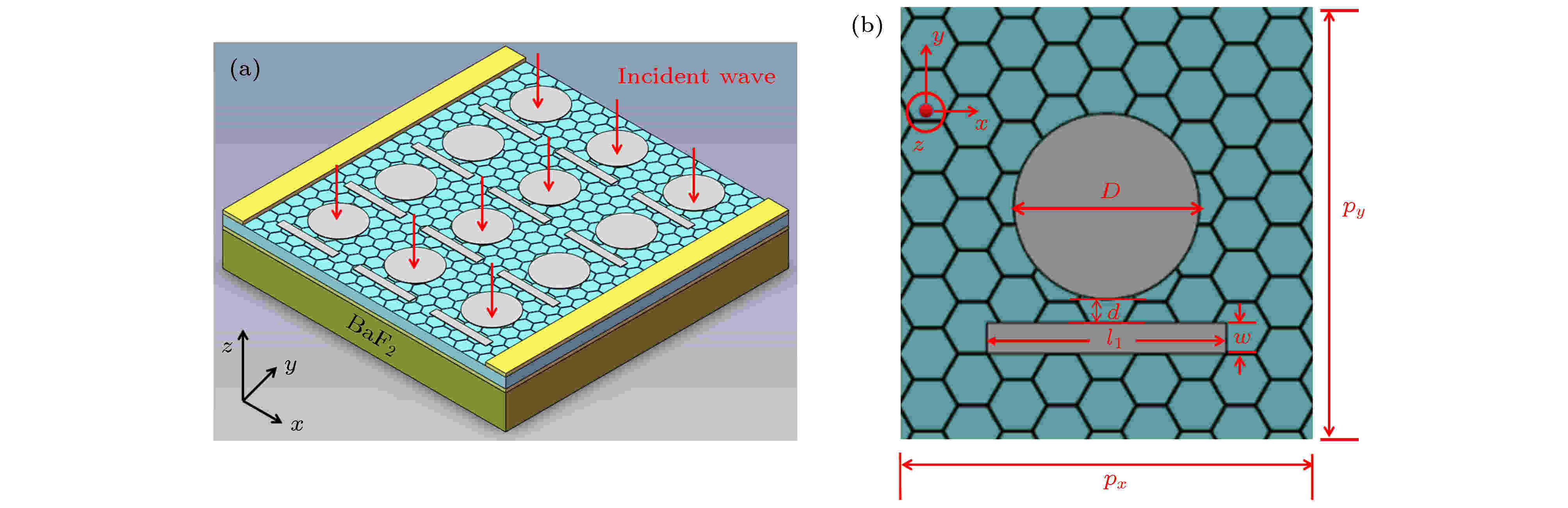
Using the Delude model. we theoretically calculate the dispersion of conductivity with frequency in the orthogonal direction of the two-dimensional black phosphorus (2D BP) x and y direction in the THz band. We find that the conductivity in the x direction is more sensitive to the electron doping concentration. The difference between 2D BP conductivities in both directions leads to the difference in dielectric constant which in turn can modulate light in different polarization directions. Using 2D BP to polarize the THz wave, the 2D BP-SiO2 periodic sandwich structure is designed. The three-dimensional electromagnetic field simulation software CST Microwave Studio can be used to calculate the regulation characteristics of this structure to THz wave. It is found that this structure has different polarization directions, and the incident THz wave has different absorption. By changing the thickness of the underlying SiO2 layer in the structure it is found that the absorption rate of this structure also changes accordingly. When the polarization direction of the THz pulse is parallel to the x axis, the absorption rate first increases and then decreases. When d5 = 9.5 μm, the absorption rate reaches 93% near 3.86 THz; when the polarization direction of the THz pulse is parallel to the y axis, the absorption rate gradually increases. The absorption peak has a significant red shift.

2020, 69 (17): 174206.
doi: 10.7498/aps.69.20200336
Abstract +
It is interesting that the electronic spin gap is opened in the localized states of nanosilicon doped with oxygen, where spin splitting of the individual two-level ±1/2 states isolated in the localized states increases by 1−2 order of magnitude (on the order of 100 meV). The opening spin level effect in the localized states is observed in experiment, which originates from the twin states of quantum vibration measured in the photovaltaic system consisting of the quantum dots and the quantum layers of silicon prepared by using a pulsed laser in an oxygen environment. The opening spin level effect in the localized states is investigated by using density functional theory (DFT) in the simulation models of the quantum dots and the quantum layers of silicon with Si=O bond or Si—O—Si bond on surface. The detailed simulating calculations show that the broader splitting gaps of the electronic spin polarization confined at the individual impurity atoms occur in the localized states, which are consistent with experimental results. A physical model is built to explain the opening spin levels effect, in which the opening spin level effect mechanism in the localized states originates from the quantum confinement at doping atom. The opening spin level effect will improve the fidelity of information stored and processed within such a spin qubit.

2020, 69 (17): 174207.
doi: 10.7498/aps.69.20200087
Abstract +
Excimer laser is the current mainstream source of international semiconductor lithography. The stable operation of the laser system directly affects the working efficiency of the semiconductor lithography machine, so it is very important to optimize the laser system. The buffer gas commonly used in ArF excimer laser systems is He, Ne. In the early years, Shinjin Nagai and Mieko Ohwa have studied the output characteristics of the system when using He or Ne as a buffer gas from the aspect of pump efficiency and gain coefficient, and pointed out that using Ne instead of He has no obvious advantages in terms of efficiency. However, when Ne is used as the buffer gas, the reaction between Ne and electrons is more complicated. In addition to direct ionization and excitation reactions, it also contains a large amount of step ionization and secondary ionization, which releases free electrons. The stability of the system is improved, when Ne is used as the buffer gas. The ArF excimer laser system discharge characteristics in different buffer gases are analyzed based on fluid model in the paper. The role of photoionization is discussed. The simulation results show that the width of the electron depletion layer and the cathode sheath are both smaller, and the discharge stability is higher when Ne is used as the buffer gas. The expansion of the discharge region is accelerated and the threshold voltage of the discharge is reduced by adding Xe into Ne to trigger photoionization. The excimer laser discharge process is very complicated and is affected by many factors. Only two factors of the buffer gas and the photoionization process are studied in this paper. The simulation model will be extended from one-dimensional case to two-dimensional case in the future, and multiple physical factors of the ArF excimer laser system will be considered.

2020, 69 (17): 174208.
doi: 10.7498/aps.69.20200482
Abstract +
The laser-induced damage to potassium dihydrogen phosphate (KDP) crystal restricts the development of high power laser systems and attract the attention of researchers. The defects are essential for the understanding of the laser-induced damage to KDP crystals. The defects in KDP crystals are commonly related to $ \rm H_2PO_4^{-} $ groups. The defects of KDP crystal have been studied extensively, however the changes of defects of KDP crystal with low fluence and high fluence have not been investigated sufficiently. The synchrotron radiation technology is a sensitive method of detecting the defects. The vacuum ultraviolet photoluminescence (PL) emission spectra can provide microscopic structural changes in KDP crystals. In this work, we investigate the defects of KDP crystals irradiated with different fluences by vacuum ultraviolet PL emission spectra. The vacuum ultraviolet spectra are obtained at the 4B8 beam line in Beijing synchrotron radiation facilities. Each KDP crystal spectrum is measured from 200 to 400 nm and 400 to 800 nm. The emission spectra of KDP crystal irradiated with different fluences are fitted for illustration. Each Gaussian curve represents a kind of defect. Comparing the retired components with KDP crystal irradiated by 11.5 J/cm2, the new band at 231.55 nm emerges in the spectra of KDP crystal irradiated by 9.0 J/cm2. The intrinsic luminescence band is assigned to the radiative annihilation of self-trapped excitons. According to our previous work, the short chain structures mainly exist in the crystal irradiated by 9.0 J/cm2, and the long chain structure is mainly in the crystal irradiated by 11.5 J/cm2. The retired components have the short, medium and long chain. The length of P—O bond in the short chain is shorter than that in the long chain structure. The overlap between phosphorus 3s orbitals and oxygen 2p increases, and the radiative annihilation of STEs becomes stronger. So the band at 231.55 nm emerges in the spectrum of KDP crystal irradiated by 9.0 J/cm2. It suggests that the structure of the retired component and the structure of KDP crystal irradiated by 9.0 J/cm2 are different. The results provide an insight into the defects in KDP crystals. It is meaningful to study the mechanism of laser-induced damage to KDP crystal.

2020, 69 (17): 174701.
doi: 10.7498/aps.69.20200073
Abstract +
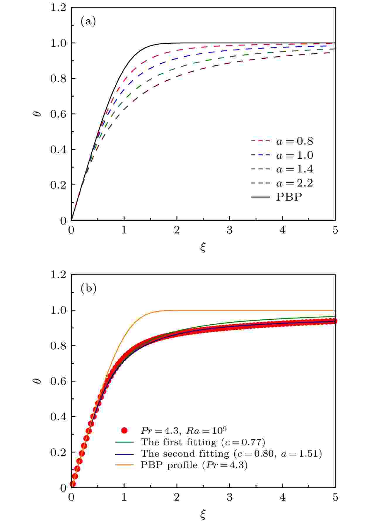
The two-dimensional thermal convection with three-Pr series Ra number is calculated by using the highly efficient parallel DNS method. The two-parameter temperature boundary layer theory, with the pulsation influence taken into account, is used to fit the temperature boundary layer profile for the field averaged over all calculations. The distributions of the fitted parameters a and c are obtained. Parameter a determines the basic characteristics of the temperature profile, and parameter c plays a role in correcting the outer area of the temperature profile. Therefore, the simulation results of the temperature boundary layer profile is well matched with the theoretical solution in the 5 boundary layers. The variation characteristic of parameter c is the opposite to that of parameter a, and the c value decreases as the a value increases. The fitting parameters for the different Pr numbers have different distribution characteristics as the Ra number changes, but they have all suddenly decreasing interruptions, and as the Pr number becomes large, the characteristic Ra number for the interruption increases. The variation characteristic of parameter c is the opposite to that of parameter a. With the same Ra number, the larger the Pr number, the smaller the fitting parameter of the temperature profile is, indicating that the influence of pulsation in the temperature boundary layer is smaller. The heat transfer characteristic Nu/Ra0.3, the large-scale circulation path circumference for the characteristics of plume movement, and the temperature boundary layer fitting parameter all have the interruptions with the change of Ra number, and their corresponding characteristic Ra numbers are identical. The results show that the three have good correlation and are directly related to the change of flow pattern.
PHYSICS OF GASES, PLASMAS, AND ELECTRIC DISCHARGES

2020, 69 (17): 175201.
doi: 10.7498/aps.69.20200468
Abstract +
The study about the wave mechanism of magnetized dusty plasmas has important value to related experiment, industrial processing and exploring celestial space. The linear and nonlinear fluctuation characteristics of the nonuniform magnetized dust plasma system are researched in this paper. For the homogeneous external magnetic field and the nonuniform environment with density and temperature gradients, a two-dimensional nonlinear dynamic magnetoplasma equation is derived considering the strong impact between dust and neutral particles. The linear dispersion relation is obtained by the linearized method. There are both the damping wave causing by strong collision and the harmonic wave by particle drift. Employing the typical numerical parameters for analysis, the results display that the quantum parameter modifies the system lengths; the real wave frequency is proportion to the drift frequency; the imaginary wave frequency has complex relationship with the collision frequency between dust and neutrals, and the collision of particles causes the dissipation effects to the system. Besides, the analytical solutions of drift shock wave and explosive wave are solved by function change method. The variation about the electrostatic potential with the main physical parameters is discussed in detail. It is shown that the strength of the electrostatic shock wave and the width of the explosive wave increase with increasing the dust density and magnetic field intensity, decrease with increasing the collision frequency, change with the drift velocity. When the space-time phase is small, the electrostatic potential changes quickly; once big enough, the potential tends to be stable value and reaches stable state eventually. Finally, the stability of the system is discussed. It is found that the dusty charge, quantum parameter, drift velocity all appear in the disturbed solution. All these results in the paper show that the strong collision effect, quantum effect, particle drift and magnetic field all play important role to the generation, evolution and stability of drift waves.
2020, 69 (17): 175202.
doi: 10.7498/aps.69.20200215
Abstract +
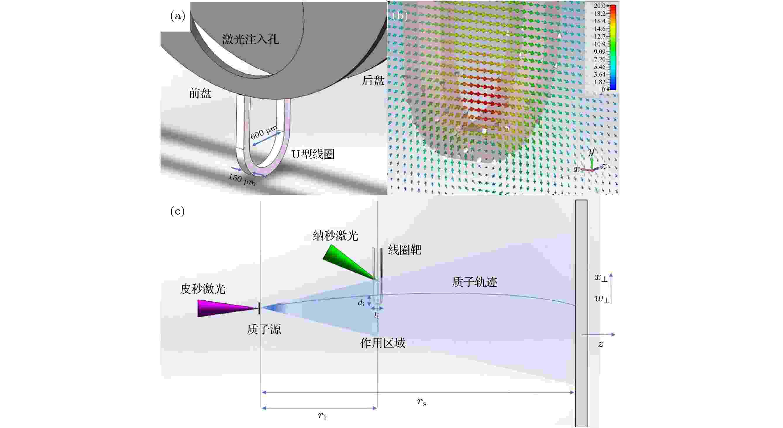
Proton radiography is a widely used method to diagnose the electromagnetic field of plasma. When protons pass through the electromagnetic field of plasma, they are deflected by Lorentz force and redistributed on the recorder. How to reconstruct electromagnetic field from the experimental result is an open problem. In this paper, we take the laser-driven capacitor-coil target for example to introduce and compare particle tracing and flux analysis, which are two widely used methods in proton radiography experiment to reconstruct the magnetic field. The capacitor-coil target is an important method to generate strong magnetic field in laser plasma experiment, where the strong current flows in the coil and its producing magnetic field may be larger than kilotesla. Firstly, the theoretical magnetic fields of capacitor-coil target are calculated with current being 10 kA and 50 kA. Secondly, the Geant4 is used to simulate the proton radiographs, where protons with 7.5 MeV pass through the target and the theoretical magnetic field is recorded. Thirdly, the theoretical proton radiographs are analyzed by the flux analysis method, and two magnetic fields are reconstructed. Finally, the theoretical magnetic fields are compared with the reconstructed ones, and the advantages and disadvantages of these two methods are analyzed. Particle tracing rebuilds the geometry distribution of proton source, plasma magnetic field and recorder in experiment, and it needs few assumptions. However, it strongly relies on accurate calculation of theoretical magnetic field and proton trajectory, and it requires to change the magnetic field over and over to achieve a closest result to the experimental proton radiograph. Meanwhile, particle tracing method consumes a lot of computation sources. The flux analysis directly reconstructs the magnetic field from experimental proton radiograph. However, it is only applicable to the case of weak magnetic field, and the error becomes larger for the case of stronger magnetic field. A dimensionless parameter μ is used to estimate the deflection of proton in the magnetic field, which measures the amount of deflection per unit length in the interaction region. The flux analysis method is applicable to the $\mu\ll 1$ regime. Additionally, the target may absorb the proton when the energy of proton is low and produces shadow on the proton radiograph, which leads to some difference between the original magnetic field and the reconstructed result.

CONDENSED MATTER: STRUCTURAL, MECHANICAL, AND THERMAL PROPERTIES

2020, 69 (17): 176101.
doi: 10.7498/aps.69.20200318
Abstract +
The dynamics of RDX single crystal under ramp wave loading is studied experimentally and numerically. The ramp wave loading experiments on RDX single crystal in the orientation of (210) and (100) within 15 GPa are carried out with the magnetic driven device CQ-4, which can provide a loading pressure waveform with a rising time of 450–600 ns. The particle velocity curves of the interface between RDX single crystal and LiF window are obtained with the photonic Doppler velocimetry (PDV). The velocity profiles show an obvious three-wave structure, indicating that the RDX undergoes physical processes such as elastic-plastic transition and α-to-γ phase transition in the loading section. The stress yield limits of different crystallographic orientations of RDX single crystal show obvious difference. The onset phase transition pressures in two crystallographic orientations are the same, which is between 3.5 GPa and 4.0 GPa. The pressure range of phase transition is between initial phase transition pressure and 5 GPa. The γ phase is stable from 5 GPa to 15 GPa. The Hayes multi-phase equation of state and non-equilibrium phase transition kinetic model are employed to simulate the experimental process, and the numerical results can well describe the experimental physical processes such as elastoplastic transformation and phase transformation in the loading section. The calculated results reveal that the correction of the bulk modulus with pressure is necessary under ramp wave compression.
CONDENSED MATTER: ELECTRONIC STRUCTURE, ELECTRICAL, MAGNETIC, AND OPTICAL PROPERTIES
EDITOR'S SUGGESTION
2020, 69 (17): 177102.
doi: 10.7498/aps.69.20200497
Abstract +
2020, 69 (17): 177103.
doi: 10.7498/aps.69.20200359
Abstract +
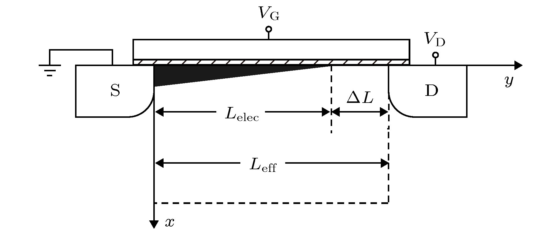
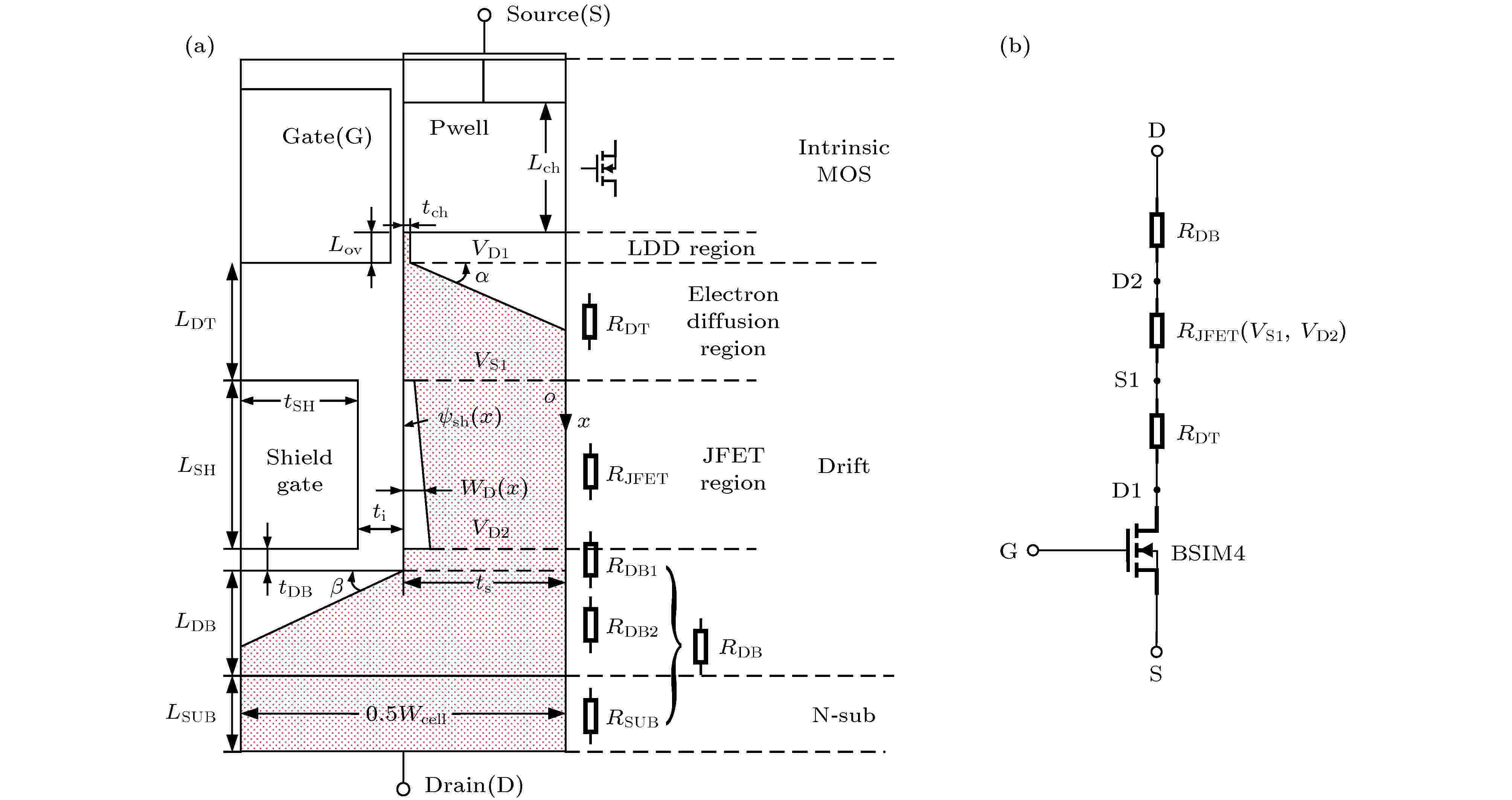
Shield-gate trench MOSFET in a low-to-medium voltage range (12-250 V) plays a key role in the power conversion market due to its low power loss caused by the sheild-gate structure. In order to eliminate the faults resulting from the parasitic effects of the device and improve the conversion efficiency, the device model is indispensable in designing a circuit system. In this paper, a compact model of shield-gate trench MOSFET based on BSIM4 is proposed, including the DC model and the capacitance model. In the DC model, the basic MOSFET structure uses BSIM4, and the equivalent resistances of the basic MOSFET in series are divided into three parts. The equivalent resistance model of JFET region is established by using the electric potential difference between both ends for the first time, and the equivalent resistance model of electron diffusion region is also introduced, in order to solve the problem of current error caused by neglecting the source potential of JFET region. The equivalent resistance between drain and JFET region and the equivalent resistance of electron diffusion region both prove to be constant. In the capacitance model based on BSIM4, the model of shield-gate to drain capacitance is added to the model of drain to source capacitance, and the voltage bias between drain and gate in the model of gate to drain capacitance is modified into the potential difference between the node at the end of the gate-drift overlap region and the gate. Poisson equations are used to solve the electric potential of this node. Furthermore, the gate oxide thickness factor k1, the shield-gate oxide thickness factor k2, the equivalent length of gate-drift overlap Lovequ and the equivalent length of shield-gate LSHequ are introduced to redefine the position of gate and shield-gate, thereby simplifying the Poisson equations and ensuring the smoothness of the potential curve of the node. Comparison of the data from the simulation by using Verilog-A program with the test results from the experimental platform shows that the model simulation results fit well with the test data, Therefore, the proposed model is verified.
2020, 69 (17): 177301.
doi: 10.7498/aps.69.20200305
Abstract +
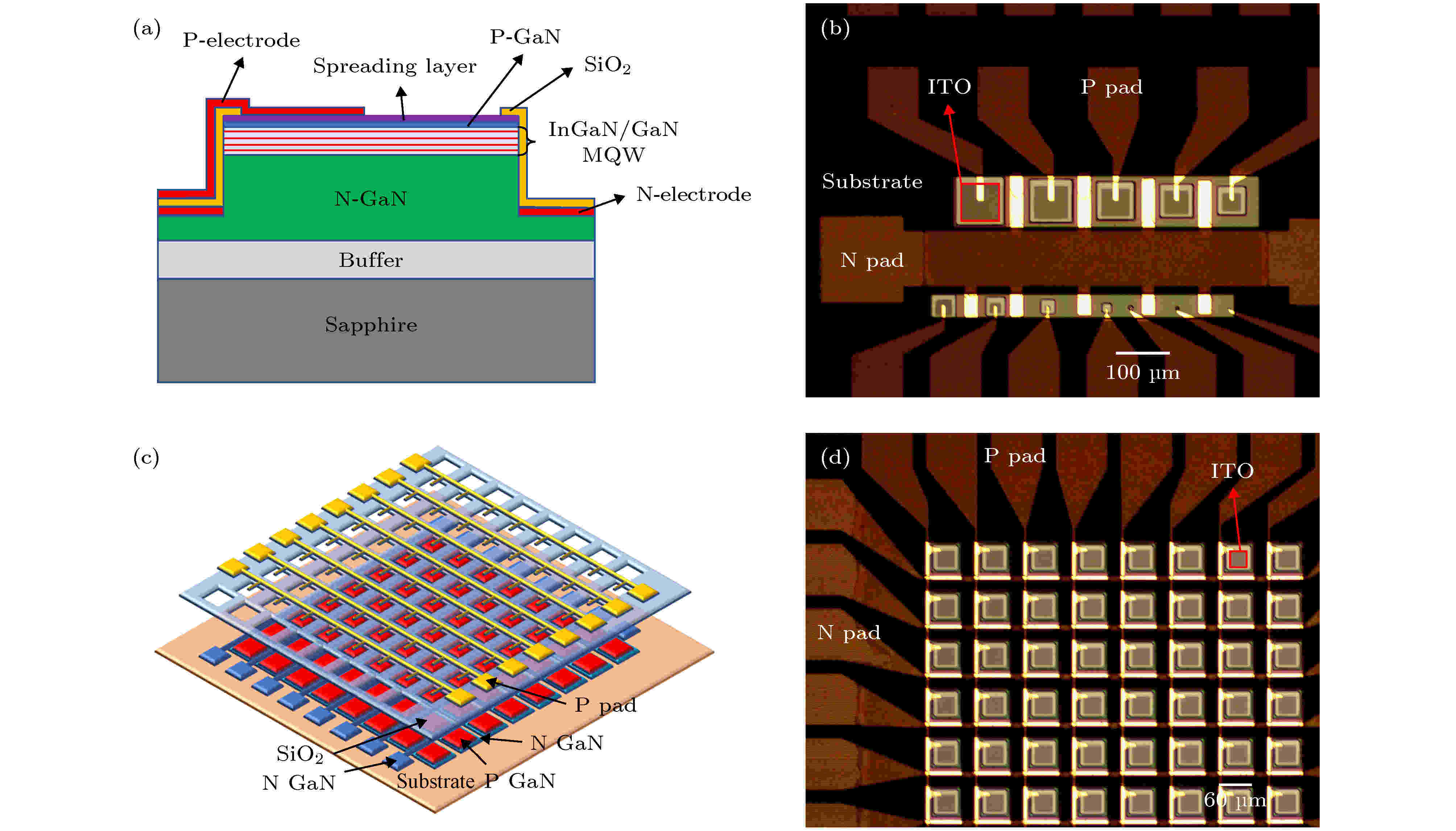
Single micro-light emitting diodes(LEDs) with different sizes and array micro-LED are designed and prepared, where the sizes of the single micro-LEDs are in a range of 40−100 μm, their electrodes are all co-N electrodes, P electrode is drawn out alone; the number of array pixels is $ 8\times8 $ , which is a passively driving structure with a pixel size of 60 μm. In the process of device preparation, N electrode and P electrode are fabricated by the sputtering & stripping method. The electrode thickness is 2.4 μm. Thick photoresist 5120 is used as a mask, and N GaN is etched to the substrate by using the ICP dry etching to form an isolation trench. The PECVD technique is used to deposit an SiO2 insulating layer with a thickness of 10000 Å. By optimizing the electrode structure and thickness, the reliability of the P electrode at the slope of the isolation trench is improved, and the SiO2 insulating layer has good encapsulation; field programmable gate array (FPGA) is used to drive and display the micro-LED passive array. The single micro-LEDs of different sizes are tested and analyzed in the aspects of electrics, photics and thermotics and the results of which show that the current density corresponding to the peak radiation flux of 80 μm micro-LED is 1869.2 A/cm2, which is 57.1% higher than that of 100 μm micro-LED, indicating that the current density corresponding to the peak radiation flux of micro-LED increases as the size decreases; compared with the ordinary blue LED, the micro-LED has a large k factor, and with the size decreases, the value of the k factor increases, indicating that the micro-LED series resistance is larger, and the thermal stability is not so good as the traditional blue LED. Finally, the field programmable gate array (FPGA) can achieve a good drive for the micro-LED passive array. The driving principle is passive scanning driving, which is carried out in a row-by-row lighting mode. The FPGA clock is 50 MHz, and 320 ns is required for the circuit to scan all rows.

INTERDISCIPLINARY PHYSICS AND RELATED AREAS OF SCIENCE AND TECHNOLOGY
2020, 69 (17): 178101.
doi: 10.7498/aps.69.20200555
Abstract +
