Vol. 69, No. 16 (2020)
2020-08-20
REVIEW

EDITOR'S SUGGESTION
2020, 69 (16): 164201.
doi: 10.7498/aps.69.20200357
Abstract +
Digital holographic microscopy (DHM) can obtain biological parameters and morphological information of cells by reconstructing holograms, which is different from traditional optical microscopy. The DHM is a three-dimensional imaging technology which is effective, non-contact and non-destructive. With the developments of the image sensor and the computing technology, it has made significant progress in the field of living cells detection, especially for red blood cell. Compared with the technologies which are widely used in the field of cell imaging such as con-focal laser scanning microscopy, scanning near-field optical microscopy and optical coherence tomography, the DHM has the advantages including wide FOV and high-resolution to achieve higher imaging and quality. This paper introduces the principle of recording and reconstruction of digital holography, and then analyzes the performance of three reconstruction algorithms using the Fresnel method, the convolution method and the angular spectrum method. The Fresnel method is suitable for the sample size larger than the image sensor. Both the convolution method and the angular spectrum method have an optimal reconstruction distance. When the reconstruction distance is different from the optimal distance, the resolution of the reconstructed image will decrease, and the angular spectrum method is better than the convolution method in overall performance. The DHM system for RBC measurements mainly adopts the convolution algorithm or the angular spectrum algorithm to implement numerical reconstruction. The systems of the in-line DHM, the off-axis DHM and the optical tweezers combining with off-axis DHM are introduced. These techniques use algorithms including Rayleigh-Sommerfeld back-propagation, the sharpness quantification, the watershed segmentation, the numerical refocusing and the thermal fluctuation to determine the focal plane position and obtain the best reconstruction distance of the RBCs, and further detect the shape change of the RBCs and extract the information of high-resolution blood vessel shape and blood flow velocity. These techniques can even achieve the dynamic tracking and measure three-dimensional volume of RBCs in real-time which is helpful for pathological studies such as diabetes, cardiovascular disease and Parkinson's disease. With its unique non-contact and non-destructive characteristics, the DHM realizes real-time and quantitative detection that is difficult to achieve with traditional three-dimensional microscopic imaging technologies.
2020, 69 (16): 167804.
doi: 10.7498/aps.69.20200591
Abstract +
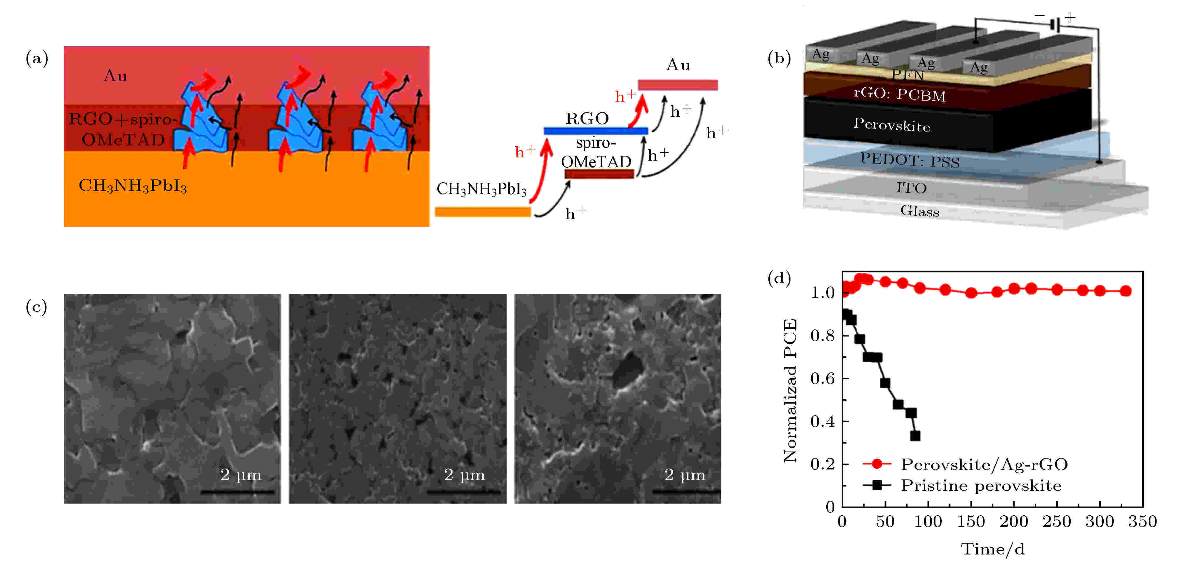
Perovskites are widely used in various kinds of optoelectronic devices, including solar cells, photodetectors, light-emitting diodes, etc., due to their excellent properties such as long carrier diffusion length, high absorption coefficient, low trap state density and so on. Functional materials such as layered two-dimensional materials (graphene, transition metal dichalcogenides, etc.),low-dimensional semiconductor nanostructures (nanoparticles, quantum dots, nanowires, nanotubes,nanorods,nanopieces,etc.), metallic nanostructures(Au,Ag, etc.) and insulating materials (insulating polymer, organic amine, inorganic insulating film, etc.) have attracted more and more attention due to their special chemical, electrical and physical properties.In order to broaden the application of perovskites in photovoltaic devices, perovskites can be combined with various functional materials to form heterostructures so as to combine the advantages of the two types of materials.The heterostructures of perovskites/functional materials can be used as the interface modification layer in halide perovskites photovoltaic devices, to improve the crystallinity of perovskite, effectively reduce the surface defects and suppress the carrier recombination loss at the interface. The heterostructures of perovskites/functional materials can be used as the charge transporting layer in halide perovskites photovoltaic devices, can match well with the perovskite energy levels, which is beneficial to the efficient extraction of holes and electrons. The heterostructures of perovskites/functional materials also can be used as encapsulation layer in halide perovskites photovoltaic devices, to reduce the contact between water and perovskite, it can effectively prevent the degradation of perovskite, to improve the device stability.In addition, the semiconductor with narrow bandgap or array structure can be used to broaden the spectral response and to improve the light absorption of the perovskite photovoltaic devices.In a word, the heterostructures of perovskites/functional materials are applied to devices is an effective way to obtain high performance and low cost photovoltaic devices.In this review, recent works on the applications of the heterostructures in halide perovskite photovoltaic devices are comprehensively presented and discussed. The progress and advantages of the heterostructures as the interface modification layer, charge transporting layers and encapsulation layer in halide perovskite photovoltaic devices are systemically reviewed. Finally, we summarize the whole paper and give a prospect for the development of heterostructures based perovskite photovoltaic devices in the future.
GENERAL

2020, 69 (16): 160201.
doi: 10.7498/aps.69.20191722
Abstract +
Attributed to facile fabrication, low production costs and outstanding photoelectric properties, dye-sensitized solar cells (DSCs) have attracted widespread attention in recent years. In order to achieve better photoelectric conversion efficiency of the DSCs, a series of TiO2 nanocomposite photoanodes co-doped with different amounts of hybrid SiO2@Au nanostructures and certain amount of graphene are prepared by a mechanical ball milling method. The influence of SiO2@Au nanostructures and graphene on the performance of the photoanodes and their DSCs were investigated. The Au nanoparticles can remarkably enhance the short-circuit current density (Jsc

2020, 69 (16): 160301.
doi: 10.7498/aps.69.20200333
Abstract +
Information security is the cornerstone and lifeblood of national security in the information society, and anonymous quantum communication is one of the important ways to protect information security. Using quantum walk randomness to effectively solve sensitive problems such as leakage of identity information. In this paper, an anonymous communication scheme based on quantum walks on the Cayley graph is proposed. First, both parties in the communication hide their identity information, and the sender Alice anonymously selects the receiver Bob through logic or operation. Secondly, the trusted third party and the communicating parties use the BB84 protocol to generate and distribute the security key. Alice encrypts the information sequence according to the security key to obtain the blind information; Bob uses the joint Bell state measurement and security key to sign and the trusted third party verifies the signature information. Third, the trusted third party calculates the position probability distribution function of Bob’s quantum walk via the Fourier transform, converts the position information corresponding to the maximum probability into a confirmation frame and sends it to Alice; Alice uses the quantum compression algorithm by decreasing dimensions to reduce the number of transmitted information bits(the length of the information bit can be reduced by up to 37.5%) and uses the security key to complete the information encryption and then transmit the information to the location indicated by the confirmation frame. Bob uses quantum walks to search the location node to obtain the transmission information and complete the anonymous quantum communication. Finally, the security analysis of the scheme is carried out, and the numerical simulation results of the Cayley graph of 200 nodes are given. At the 10-step walk, the maximal probability of the 6th node is 45.31%. According to the simulation results, the probability that Bob is eavesdropped on the specific location at his 10-step walk during the communication of this scheme is approximately 6 × 10⁻⁷%, so the receiver can avoid the identity information from the eavesdropping with a high probability, and the quantum network anonymity protocol is not broken.
2020, 69 (16): 160501.
doi: 10.7498/aps.69.20191642
Abstract +
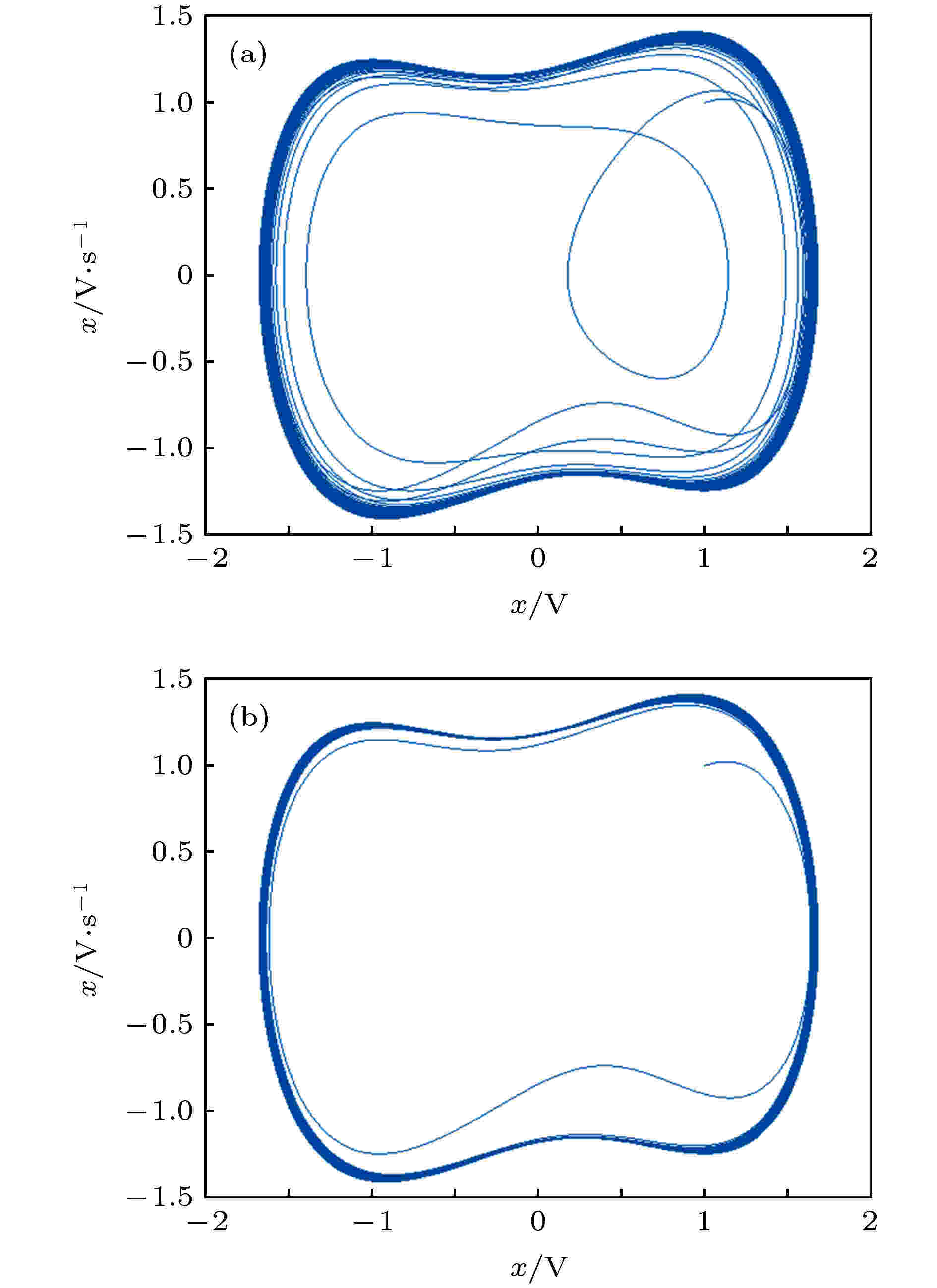
Entropy is one of the parameters describing the state of matter in thermodynamics, it can be used to measure the degree of confusion. The entropy of the signal can be used to express the complexity of the signal. The threshold for the transition of the Duffing chaotic system from the critical chaotic state to the large-scale periodic state is called the transition threshold. It is an important parameter for the analysis of chaotic systems, and its solution method is one of the problems urgently to be solved in chaos theory. If the jump threshold is smaller than the real threshold of the system, it will affect its detection signal-to-noise ratio. If the jump threshold is larger than the real threshold, it will cause incorrect detection results, so it is very important to accurately determine the jump threshold. In this study, we found that the multiscale sample entropy value of the Duffing system is significantly different when the system is in the chaotic state and the periodic state, when the system is in a chaotic state, the entropy value is larger, when the system is in a periodic state, the entropy value is smaller, and when the system enters the periodic state, the multiscale entropy value tends to be stable, this paper proposes to use this phenomenon to determine the transition threshold by analyzing the relationship between the entropy of the system and the amplitude of the driving force. When the entropy value is obviously smaller and tends to be stable, the corresponding driving force amplitude is the jump threshold. using this method, the jump threshold of the sinusoidal signal and square wave signal detection system is calculated, the results show that the method is fast, accurate and simple to calculate. However, this method may have a problem that the calculated threshold value is smaller than the real threshold value, our analysis is that the random selection of the subsequence used for calculation causes the calculation threshold value to be too small, so the method is improved in conjunction with genetic algorithm, using genetic algorithm to find the most complicated subsequence in the whole sequence, then this subsequence is used to solve the threshold, Through a large number of calculations and analysis, it can be seen that the problem of a small threshold is no longer present, and the improved method can obtain the jump threshold of the Duffing system very accurately.
NUCLEAR PHYSICS

EDITOR'S SUGGESTION
2020, 69 (16): 162101.
doi: 10.7498/aps.69.20191643
Abstract +
Based on the existing experimental data of nuclear radius, the previous formula of nuclear charge radius is verified and discussed. Comparing the formula of the single-parameter nuclear charge radius, it is proved that the formula of $Z^{1/3}$ law is better than the formula of $A^{1/3}$ law. We refitted the two-parameter formula and the three-parameter formula that have been proposed and confirmed that the two-parameter and three-parameter formula fit better than the single-parameter formula. It is shown that show that the deformation plays a key role in the nuclear charge radius. The electric quadrupole moment is an important physical quantity representing the properties of the nucleus. Its appearance indicates the deviation from spherical symmetry and also reflects the size of the nuclear deformation. The electric quadrupole moment is also one of the basic observations to understand the distribution of matter within the nucleus, to examine the nuclear model, and to observe nucleon-nuclear interactions. Taking into account the relationship between the nuclear quadrupole moment and the deformation, the electric quadrupole moment factor is added to the original three-parameter formula to obtain a new formula for the nuclear charge radius. Fitting the four-parameter formula, it is found that the theoretical value of the nuclear charge radius is in good agreement with the experimental value, the root-mean-square deviation is 0.0397 fm. Considering the relationship between the total spin and the electric quadrupole moment, the intrinsic electric quadrupole moment is obtained and brought into the formula for fitting, and the root-mean-square deviation further decreases,the root-mean-square deviation is 0.0372 fm. Finally, considering the universality of odd-even staggering, we add the $\delta$ term that can reflect the odd and even oscillation phenomenon, and the root-mean-square deviation obtained by the formula is 0.369 fm, which better reflects the relationship between the deformation and the nuclear charge radius. Compared with the formulas already proposed, the new formula can better reflect the variation trend of nuclear deformation, shell effect, odd-even staggering, etc., and the calculation accuracy is also improved, which can provide a useful reference for future experiments.

2020, 69 (16): 162901.
doi: 10.7498/aps.69.20200265
Abstract +
The experiment of neutron single event effect was carried out at China Spallation Neutron Source (CSNS) back-n on 13 kinds of commercial SRAM. The single event upset (SEU) cross section of each device was obtained, and multiple cell upsets (MCU) were extracted from the SEUs using a statistical method without layout information. The influences of the test pattern, feature size and device layout on the SEU cross section and MCU were studied. The results show that the test pattern has little influence on the SEU cross section of the devices, but has a great influence on the MCU ratio of some devices. The feature size has influence both on the SEU cross section and the MCU ratio of the devices. The influence on SEU cross section is not definite. The influence on the MCU ratio is definite. Both the ratio and the maximum size of the MCUs increase with the decrease of the feature size. The difference of layout has great influence both on the SEU cross section and the MCU ratio of the device. In addition, compared with the results of plateau irradiation, the ratio of MCU in CSNS back-n is less than that of plateau irradiation. There are two reasons for this difference. One is that the energy spectrum of CSNS back-n is softer than that of the atmospheric neutron. The other is the neutron beam at CSNS back-n is perpendicular to the device under test. Therefore, evaluating the atmospheric neutron SEE using CSNS back-n line may underestimate the MCU ratio of the device under test. The experimental data, analytical methods and results obtained in this paper are valuable for the researchers to carry out the atmospheric neutron SEE test and the evaluation of devices on atmospheric neutron SEE.
ATOMIC AND MOLECULAR PHYSICS
2020, 69 (16): 163101.
doi: 10.7498/aps.69.20200518
Abstract +
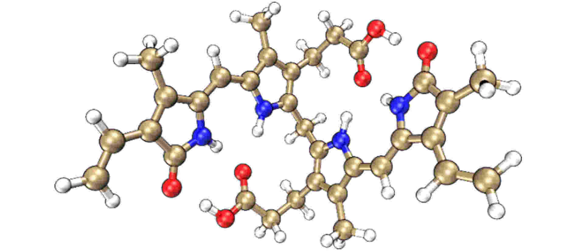
Bilirubin is the main pigment in human bile, which is closely related to human health. Bilirubin combining with fluorescent protein represents a new type of fluorescent chromophore and has important applications in the field of biological imaging and biosensor. Due to the lack of efficient and accurate electronic structure methods, the electronic structure and excited-state properties of bilirubin molecule are not characterized quantitatively and accurately. Firstly, the vertical absorption energy, oscillator strength and vertical emission energy of the lowest singlet excited state of bilirubin molecule are calculated by combining the implicit solvent model and the linear response time-dependent density functional theory (TDDFT) method. Compared to the experimental data and high-level RI-ADC(2) calculation, the prediction performance of a series of density functional methods is systematically investigated. The results show that the optimally-tuned range separated density functional method has the best overall performance and the minimum absolute and relative errors. This is obviously due to the fact that the suitable proportion of exact exchange included in density functionals can produce neither delocalized nor localized electronic structures. Based on the produced wavefunction by the optimally-tuned method, the excited-state characteristics of the S1 state of bilirubin molecule indicate a hybrid local and charge transfer excitation, based on the quantitative characterization using hole-electron analysis and interfragment charge transfer method. This work can provide a theoretical basis for the study of excited-state dynamics and spectral properties of bilirubin molecules and the optimally tuned range-separated DFT method also provide a reliable and efficient theoretical tool to study the excited-state properties of other biomolecular systems in the future.

2020, 69 (16): 163301.
doi: 10.7498/aps.69.20200601
Abstract +
Bioelectrical impedance spectroscopy is a noninvasive, label-free and quantitative detection technology, which has great advantages in the physiological and pathological analysis of biological cells and tissues. In this paper, the relationship between the electrical properties of a single cell and its structure is studied by numerical simulation. Moreover, experiments are conducted to verify the simulation results. For simulation, three single cell models are used to express its structure. Among of the three models, No Shell Model (NS) is proposed in this paper to study the influence of cell membrane on bioelectrical impedance spectroscopy. In addition, the effects of cell type, cell membrane and cell nucleus on its electrical properties are studied by simulation based on Single Shell Model (SS) and Two Shell Model (TS). The simulation results show that: 1) the electrical characteristics of cells can reflect its structure, therefore, the cell type can be accurately distinguished by its electrical characteristics; 2) the high frequency part of the Cole-Cole Plot is caused by ionic polarization of cytoplasm or extracellular fluid, and the low frequency part of the Cole-Cole Plot is caused by interface polarization between cell membrane and the extracellular fluid; 3) the influence of cell nucleus size on impedance measurement is mainly in the low frequency range, which is caused by the polarization of the interface between cell nucleus and intracellular fluid, and when the nucleocytoplasmic ratio is less than 0.25, the effect of nuclear size on impedance analysis could be ignored. Finally, an experiment was conducted on 20% yeasts suspension with different activity to verify the simulation results. It is known that the cell membranes of dead yeasts are destroyed, however, living yeasts have completed cell structures. The structure difference between living and dead yeast is distinguished by electrical impedance spectroscopy through numerical simulation. The experimental results are consistent with the simulation results, which verifies the fact that the high frequency part of the Cole-Cole Plot is caused by ionic polarization of cytoplasm or extracellular fluid, and the low frequency part of the Cole-Cole Plot is caused by interface polarization between cell membrane and the extracellular fluid.
ELECTROMAGNETISM, OPTICS, ACOUSTICS, HEAT TRANSFER, CLASSICAL MECHANICS, AND FLUID DYNAMICS

2020, 69 (16): 164101.
doi: 10.7498/aps.69.20200271
Abstract +
As a new kind of electromagnetic pulses with finite energy, the flying electromagnetic toroid (FET), also called as the flying electromagnetic doughnut, has significant potential applications, such as the excitation of anapole non-radiation mode and the acceleration of charged particles. To show the propagation characteristic of FET, the spatial distribution and spectrum characteristic of the transverse and longitudinal components of FET and its topology evolution in the propagation process are discussed in this paper. Without loss of generality, we theoretically research the longitudinal field and transverse field of the transverse magnetic (TM) FET based on the real part of FET’s propagation equations. The field distribution, topology, and spectrum when the FET propagates to different positions can be calculated by assigning corresponding values to the time variable in FET’s propagation equations, therefore, the propagation characteristics of FET can be studied accurately in theory. The magnetic field of TM FET is distributed into rings in the plane vertical to the propagation direction and the electric field of TM FET is rotated around the magnetic field, which means the FET has a hypertorus topology. All the field components of FET are rotationally symmetric in the plane vertical to the propagation direction. The FET’s center is the maximum position of the longitudinal electric field component and the null position of the transverse electric and magnetic field components. Maximum values of FET’s longitudinal field are always located on the central line of FET’s propagation path and decrease gradually in the propagation process. Different from the longitudinal field, the maximum value of FET’s transverse field gradually moves away from FET’s center. The theoretical research indicates that the FET spreads quite slowly in its early propagation state and spreads linearly after propagating a long distance, which has the slowly spreading propagation characteristic even in the so-called focused range with stable toroidal topological structure. The further spectrum analysis shows that the high-frequency components spread less than the low-frequency components and the high-frequency components play a vital role in the topology retention of FET in the focused range, which may provide a basis for the generation and application of FET. At present, the theoretical research on FET’s characteristics is increasingly improved. To apply the attractive characteristics of FET in actual systems, it is necessary to actually generate FET. Therefore, the generation method of FET should become the next research emphasis.
2020, 69 (16): 164102.
doi: 10.7498/aps.69.20200434
Abstract +
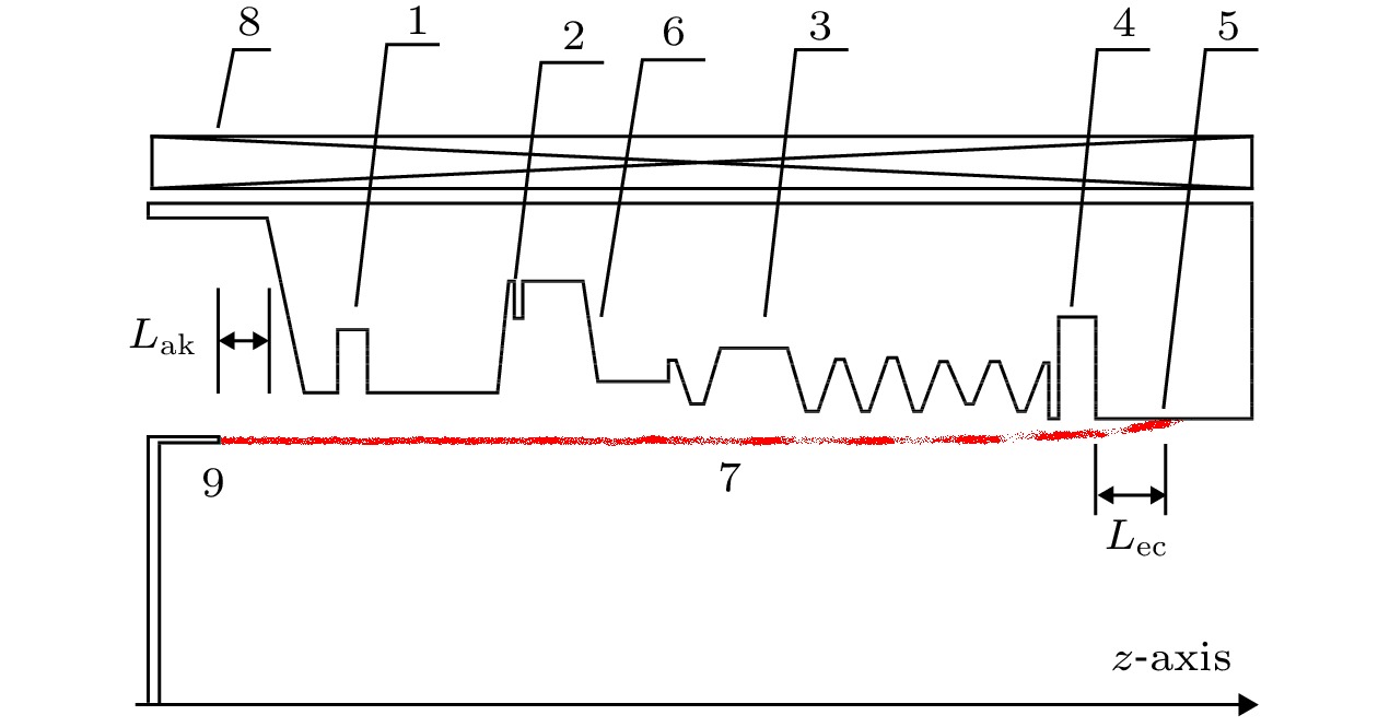
This paper investigates an X band high efficiency klystron-like relativistic backward wave oscillator (RBWO) in detail. The klystron-like RBWO consists of a pre-modulation cavity, a resonant reflector with a ridge, a sectional slow wave structure, and an extraction cavity. First, this paper gives some theoretical studies about beam modulation and energy extraction. For beam modulation, the optimized distance between the pre-modulation cavity and the resonant reflector is studied theoretically, and theoretical results agree well with simulation results. For energy extraction, an ellipse extraction cavity with high power capacity is come up with, and the electric field on the inner surface of the ellipse extraction cavity decreases by 25% in PIC simulation. Also, the paper analyzes the effect of the position of dumped electron on conversion efficiency. Interestingly, it’s found that the efficiency dramatically decreases with the increase of the distance between the extraction cavity and the position of dumped electron, which is caused by the increase of potential energy of electron and the decrease of electric field. Fortunately, we find that the use of guiding magnet with special magnetic field distribution almost eliminate this unfavorable effect. Besides, effects of the distance between the cathode and anode Lak are investigated. It’s shown that the optimized diode voltage decrease with the increase of the distance Lak, and the conversion efficiency is higher at larger Lak. The experimental studies are also given. The power capacity of ellipse extraction cavity is verified, also we find that the efficiency is enhanced by 10% and the width of microwave pulse increases by 7 ns when the roughness of RF structure surface is improved from Ra 0.4 μm to Ra 0.05 μm. Typically, the klystron-like RBWO outputs X band high power microwave with power of 2.15 GW, with pulse duration of 25 ns, and with conversion efficiency of 50%(± 5%). Experimental results agree well with theoretical and PIC simulation results.

2020, 69 (16): 164202.
doi: 10.7498/aps.69.20200245
Abstract +
We demonstrate generation of high-power and large-energy noise-like square pulses at 1612 nm in an all-fiber dumbbell-shaped mode-locked Er: Yb co-doped double-clad fiber (EYDF) laser. The custom couplers with high power handling keep the laser function well. Large-mode-area EYDF with high power handling and enough high pump power make it possible to obtain high output power in the oscillator. Compared with figure-eight structure, strictly all-fiber dumbbell-shaped structure without isolator and optimizing splicing loss could reduce intra-cavity loss and improve optical to optical efficiency, which could reduce heat accumulation and enhance the power carrying capacity of EYDF. In order to study the influence of in-band absorption on output wavelength, EYDF1 and EYDF2 with different in-band absorption coefficients are accessed to intracavity, respectively. It is directly demonstrated that regulation of in-band absorption is an effective way to control the output wavelength. Strong in-band absorption could restrain the emission of C-band and make the wavelength range above 1.6 μm obtain enough gain. Linear insertion loss is another important factor to affect the emission wavelength in EYDF fiber laser. At pump power of 8 W, maximum average output power with emission wavelength above 1.6 μm can reach 1.16 W, corresponding to a single pulse energy of 1.26 μJ. SNR of output pulse is 70 dB which indicates the high stability of mode-locking. In order to verify and evaluate influence of insertion loss on the output characteristics of mode-locked laser, a variable attenuator is inserted in experimental setup, allowing us adjust the linear loss of the cavity. By increasing pump power and adjusting PCs, mode-locked pulses could be obtained on the condition of large additional insertion loss. Even though ~ 10 dB additional insertion loss is introduced, the oscillation still could function at 1612 nm and keep stable mode-locked state. This result demonstrates our oscillation could bear strong additional loss and own strong robustness. If excessively large additional insertion loss is added, 1566 nm becomes the central emission wavelength and wavelength component at 1612 nm almost disappears. Our investigation supplies a direct guideline to design high-power fiber laser with emission wavelength above 1.6 μm.
2020, 69 (16): 164203.
doi: 10.7498/aps.69.20200418
Abstract +
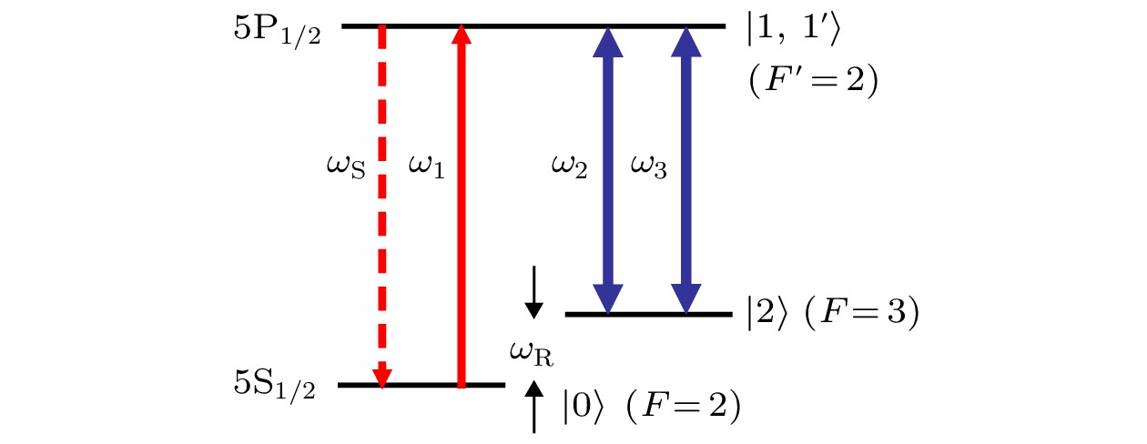
We observe experimentally huge enhanced four-wave mixing based on Raman resonance in an 85Rb atomic vapor system. With the decrease of coupling field power or the increase of experimental temperature, the signal tends to be narrowed down in linewidth, and be basically the same spectrum as the stimulated Raman spectroscopy. It is found that the macroscopic polarization interference effect plays a crucial role in determining the nonlinear spectra. Further more, in the Doppler-broadened Λ-type energy level system, there is a strong relationship among electromagnetically induced transparency, four-wave mixing and stimulated Raman spectroscopy. The sharp transparent window in electromagnetically induced transparency can be interpreted as the suppression of Raman gain on the linear absorption of the probe field. However, the four-wave mixing signal is a new field generated by the atomic vapor system, and it comes from the Raman gain which is affected and modified by the absorption and dispersion of the nonlinear optical medium. It shows that in a Λ-type Doppler-broadened system, in essence, both the electromagnetically induced transparency and enhanced four-wave mixing stem from stimulated Raman scattering based on the third-order nonlinear processes, just the spectra of which are from different ways and objects of detection.

2020, 69 (16): 164204.
doi: 10.7498/aps.69.20200396
Abstract +
An acousto-optic switch scheme based on optical tamm state (OTS) is proposed. The acousto-optic switch’s structure is one-dimensional photonic crystal heterostructure, which is composed of three materials: silicon dioxide, gallium arsenide and tellurium dioxide. All three materials are acousto-optic materials, which can ensure the acousto-optic effect when the ultrasonic wave and the light wave are incident at the same time. Due to the acousto-optic effect, the refractive index and thickness of one-dimensional photonic crystal heterostructures are changed by ultrasonic. The acousto-optic switch changes the ultrasonic amplitude to shift the intrinsic wavelength of OTS to the shorter wave direction. With the increase of ultrasonic amplitude, the intrinsic wavelength of OTS hardly changes after the amplitude exceeds 0.4 nm. This means that the ultrasonic wave with an amplitude of 0.4 nm can shift the intrinsic wavelength to 1538 nm. The acousto-optic switch realizes the on-off function within the permitted range. In this paper, the theoretical model of the acousto-optic switch is established. The propagation of ultrasonic wave in one-dimensional photonic crystal heterostructure is analyzed by theoretical model. The propagation of light in the medium after acousto-optic effect is analyzed by transmission matrix method. The simulation is carried out through COMSOL Multiphysics software. The results show OTS exists and localization can be seen in the electric field diagram. The acousto-optic switch of 1548.8–1551.7 nm can be realized by applying certain amplitude of ultrasonic or not. In this wavelength range, the extinction ratio is not lower than 12 dB and the insertion loss is not higher than 0.97 dB. The maximum extinction ratio is 13.17 dB, and the minimum insertion loss is only 0.65 dB. The acousto-optic switch of 1536.6–1543.3 nm can be realized by applying ultrasonic wave with amplitude corresponding to the length of incident light. In this wavelength range, the extinction ratio is not lower than 12 dB, and the insertion loss is not higher than 0.99 dB. The maximum extinction ratio is 13.15 dB, and the minimum insertion loss is only 0.65 dB. The response time of the acousto-optic switch is less than 13 ns. The acousto-optic switch has the characteristics of high extinction ratio and low insertion loss. It has a good application prospect and can be effectively applied in future optical communication.

2020, 69 (16): 164301.
doi: 10.7498/aps.69.20191948
Abstract +
In this paper, the modal space detector (MSD) is investigated in shallow water environment when utilizing a vertical linear array. The processing gain of the MSD is derived, and the result demonstrates that the processing gain of the MSD degrades when the number of the propagated normal modes excited by the underwater acoustic source increases, and therefore the detection performance of the MSD decreases. By exploiting the orthogonality among the modal depth functions, the MSD can be decomposed into a group of modal subspace detectors (MSSDs). The processing gains of these MSSDs are derived as well and it is found out that the processing gain of a MSSD is in direct proportion to its corresponding modal attenuation coefficients. By designing a group of weighting coefficients based on the mode attenuation law, a weighted modal subspace detector (WMSSD) is proposed to alleviate the degradation of the processing gain processing of the MSD. We analyze the influences of acoustic source locations and sound velocity profiles (SVPs) on the detection performance of the WMSSD theoretically, and verify the theoretical analyses by comparing its processing gain with the MSD in simulation experiments. The results show that the WMSSD presents various processing gains versus different acoustic source locations. In the waveguide having a negatively-gradient SVP, there exists a ‘weak detection area’ for the WMSSD, that is, the processing gain of the WMSSD is smaller than that of the MSD when the acoustic source locations are close to sea surface. The reason is because there are inversion points on the lower-order modal depth functions and the depths of the inversion points are close to sea surface. In other most areas, the processing gain of the WMSSD is larger (even remarkably larger) than that of the MSD. In the waveguide having a positively-gradient SVP, due to the phenomenon that the modal inversion points of the lower-order modal depth functions are near sea floor, there is a contrary consequence, that is, the ‘weak detection area’ is close to sea floor. And meanwhile the WMSSD outperforms the MSD in other most areas as well. There are no modal inversion points in the waveguide having a constant SVP, and therefore the WMSSD always outperforms the MSD.

2020, 69 (16): 164401.
doi: 10.7498/aps.69.20200308
Abstract +
In this work, numerical simulation of nature convection of Al2O3-H2O nanofluid in an inclined square porous enclosure is investigated to analyze the influence of different physical parameters on fluid flow and heat transfer via the lattice Boltzmann method. Due to stable chemical properties and low price in the dispersion system, Al2O3-H2O nanofluid is widely used in the field of industrial heat transfer enhancement, which is the focus of present work. When the nanofluid is transport in a porous media, the Darcy-Brinkman-Forchheimer model is usually used to describe the porous media effects on nanofluid flow. Compared with uniform thermal boundary condition, the natural convection of nanofluids with non-uniform thermal boundary condition has not received much attention. In this paper, the sinusoidal boundary condition is applied to the left side wall to analyze the heat transfer mechanism of Al2O3-H2O nanofluid in the inclined square porous enclosure. The effect of porosity (0.3 ≤ $\epsilon $ ≤ 0.9), Rayleigh number (103 ≤ Ra ≤ 106), volume fraction of nanoparticle (0 ≤ ϕ ≤ 0.04), tilt angle (0° ≤ γ ≤ 120°) on the heat transfer performance are systematically investigated. Numerical results show that the non-uniform boundary condition can affect the heat transfer performance on Al2O3-H2O nanofluid with different physical quantities, which is different from the uniform boundary condition. When γ = 0° and Ra is fixed, the Nuave number (average Nusselt number) at the heated wall increases with porosity. When γ = 40°, 80° or 120°, the Nuave reaches its maximum value at $\epsilon $ = 0.7. In addition, if $\epsilon $ and Ra are fixed, the results show that the heat transfer performance is most efficient at γ = 40° whereas it is weakened at γ = 80°. Moreover, when different inclination angles are applied to the square cavity, the Nuave increases slightly with an augmentation of ϕ. In all, compared with the uniform temperature boundary condition, the effect of volume fraction of nanoparticles on the enhanced heat transfer is not significant, therefore, to improve the heat transfer performance of nanofluids with given ϕ and Ra, it is necessary to take advantage of the improvement of effective thermal conductivity for the nanofluids in porous media and the perturbation influence of inclination angles on the system together with using appropriate porosity and square cavity tilt angle to intervene the flow.

2020, 69 (16): 164501.
doi: 10.7498/aps.69.20200223
Abstract +
Loose materials has loose structure and is the main source of geological disasters such as collapses and landslides. Its hazard range is greatly affected by factors such as stone content and slope. Traditional studies on the sliding and accumulation characteristics of loose materials were mostly macro or qualitative analysis. There is little research on the micro internal motion mechanism. In the present study, discrete element method was used to quantitatively analyze the influence of stone content and slope variation on the characteristic values of loose particles such as stroke, accumulation width, maximum thickness, accumulation area, accumulation contour shape, accumulation volume, static accumulation angle and the cumulative mass. In the meanwhile, the movement and accumulation characteristics of the loose materials during the catastrophe process were explored from the aspect of energy and contact force of the particles, so as to reveal the interaction mechanism between the particles. The results showed that: When the stone content increased in the range of 0 to 70%, the stroke, accumulation width and accumulation area increased firstly and then decreased, and in the end the cumulative mass decreased. As the slope increased from 30° to 65°, the stroke, accumulation width, accumulation area and accumulation mass increased; the maximum thickness decreased approximately linearly, while the static accumulation angle had a decrease similar to quadratic function. In addition, there was a critical distance Lc for the volume share of coarse and fine particles in the accumulation area. When the distance from the toe line was L < Lc, the fine particles were larger than the volume of the coarse particles; when L > Lc, the fine particles were smaller than the volume occupied by coarse particles.
PHYSICS OF GASES, PLASMAS, AND ELECTRIC DISCHARGES

2020, 69 (16): 165201.
doi: 10.7498/aps.69.20200517
Abstract +
Nano-scale particle stripping and inspection on silicon wafer are critical issues for Integrated Circuit(IC) manufacture industry. As more new materials are used in IC manufacture, not only particle itself but also its composition should be inspected. Particles are mainly adhered by the van der waals force. One of potential particle desorption method is laser cleaning which is environment friendly. However, the mechanism of laser cleaning is not clear and more studies should be done for laser ablation. In this paper, the kinetic process of nano particle on silicon wafer induced by nanosecond pulsed laser as well as the on-line detection method of particle composition were studied. A potential method of nano particle dynamic analysis and particle composition inspection were presented. A dual nanosecond pulse laser system both wavelengths at 532 nm is designed in which one laser pumps the particles away from wafer surface almost without damage, the other laser breakdowns the particles in air above the wafer surface to obtain the emission lines of the contaminated particles of 300 nm Cu by a spectroscopy with CCD. Particle motion trail in z direction was observed after laser cleaning by analyzing particle spectral features. The particle dynamic model after stripping was established in which the resistance of air collision and gravity were included. And the model parameters were obtained by calculation using experimental results. The initial velocity of particle at the end of laser pulse and the average acceleration during laser interaction were calculated which were 7.6 m/s and 7.6 × 10⁸ m/s2 respectively. The sensitivity of the dual laser system was evaluated which was between 2.1 × 10¹³ to 5.1 × 10¹³ atoms/cm2. As result, it is found that the gravity of the particle should not be ignored and the velocity divergence between different stripping particles is existed. The study not only provides a methodology for the study of laser-induced removal of nano particles on the wafer surface and laser induced nano particle dynamics, but also provides a potential method for the inspection of particle composition and pollution source monitoring on line in integrated circuit manufacture process. As the results were not the optimum one and further study should be done in which a better laser power density should be used.

2020, 69 (16): 165202.
doi: 10.7498/aps.69.20200095
Abstract +
Based on the principle of micro-scale discharge, the micro-nano ionization gas sensor has the characteristics of fast response, high precision and easy integration. It is expected to achieve rapid and accurate detection of gas. At present, there is a lack of systematic analysis of the inter-polar discharge process of the new sensor. This paper uses the fluid-chemical dynamics methodology to create a 2D space discharge model of the N2-O2 mixed gas at the micron gap and the nano-tip field in ambient atmosphere at normal temperature and pressure. Meanwhile, by analyzing the mutual coupling between the space electron transport process, the discharge current density, and the space electric field strength, the paper clarifies the dynamics of space discharge in the field, improves how internal discharges work in such micro-nano structured ionization gas sensors, and analyzes the pattern of influence of different polar distances on space discharges. The results show that the electric field in the space remains constant as the production and consumption of positive and negative ions reaches a dynamic equilibrium in the field. It is reflected in the field strengthening effect of positive ion groups to the cathode plate and of negative ion groups to the anode plate, as well as in the field weakening effect between positive and negative ion groups. The resulting stable and strong electric field of the cathode makes sure that space discharge is maintained, and the discharge current density stabilizes. Initially, as the polar distance decreases gradually, the electric field strength between the poles and plates increases. It plays a leading role in the accumulation of electron energy and in the increase in the number density of electrons, thus leading to the increase of the output current density up to the peak value when the polar distance D = 50 μm. As the polar distance decreases, the field strength between the poles and plates increases. Despite that, when electrons accumulate energy up to such a level that gas molecules can be ionized, the necessary movement distance and the distance required to increase the number density of electrons decreases. As a result, the degree of ionization weakens, and the field strengthening effect of positive ions decreases. In other words, the increment of the field strength caused by positive ions at the tip decreases, and in turn, the discharge current density decreases. This pattern serves as a theoretical support in the optimization of the micro-nano structured ionization gas sensors.
2020, 69 (16): 165203.
doi: 10.7498/aps.69.20200044
Abstract +
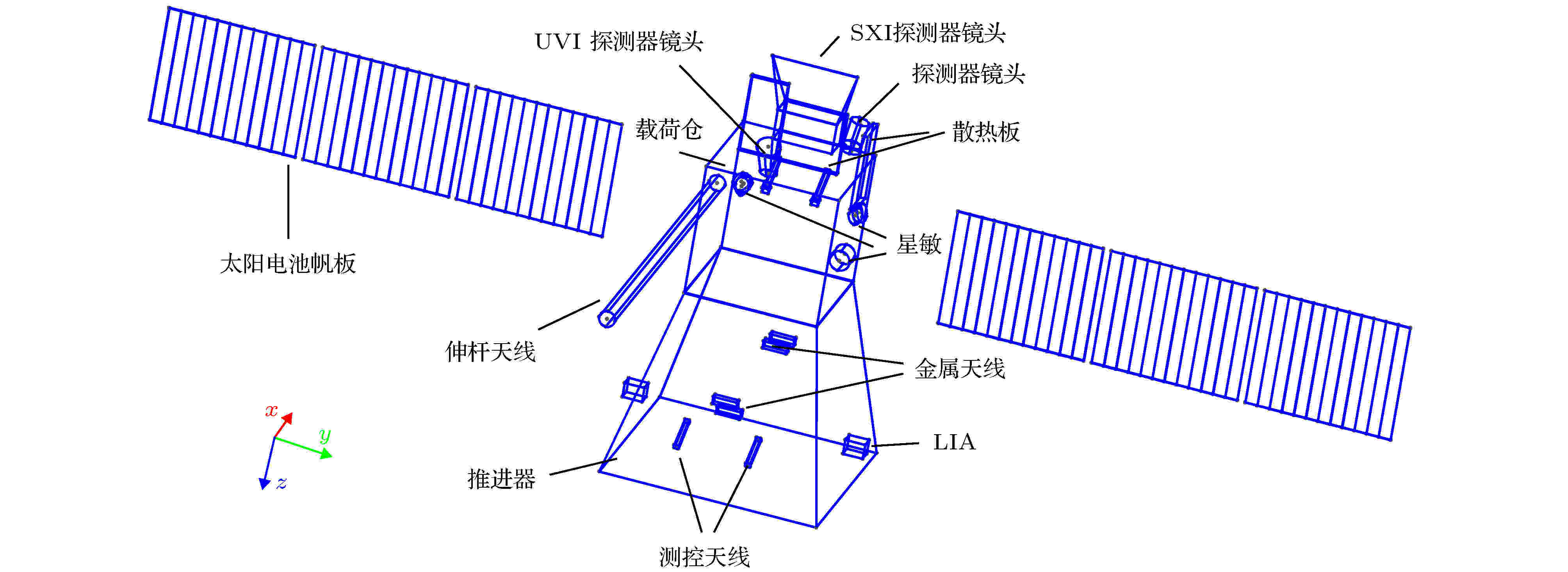
When the satellite is on orbit, the surrounding plasma environment will interact with the spacecraft surface, accumulate charges on the spacecraft surface and cause surface charging effect, which could lead to electrostatic discharge and affect the running of the spacecraft. SMILE is a satellite operating in a solar synchronous and high inclination large elliptical orbit. The on-orbit motion will encounter ionospheric plasma, magnetospheric plasma and solar wind plasma, pass through the region of the outer radiation belt enriched by high-energy electrons. These environmental factors can cause the surface charging effect on satellite and affect on-orbit security of the satellite and the acquisition of scientific data. Utilizing the software simulation of spacecraft plasma interaction system, the charging effects of SMILE satellite surface in solar wind plasma, magnetic tail plasma and extremely harsh plasma environment have been simulated, and the charging potential distribution on its surface have been obtained. The results show that the surface charging potential varies in different environments, but all comfort with the design requirements. The analysis of surface current shows that the secondary electron emission has great influence on surface charging in various plasma environments. Under sun illumination, photoelectron emission dominates surface charging. By analyzing the charge current on the surface on the eclipse, the calculated results can supply the experimental curve of the secondary electron emission coefficient of indium tin oxide materials.
CONDENSED MATTER: STRUCTURAL, MECHANICAL, AND THERMAL PROPERTIES
Study on the electronic structure and photocatalytic properties of a novel monolayer TiO2(Retracted)
2020, 69 (16): 166301.
doi: 10.7498/aps.69.20200631
Abstract +
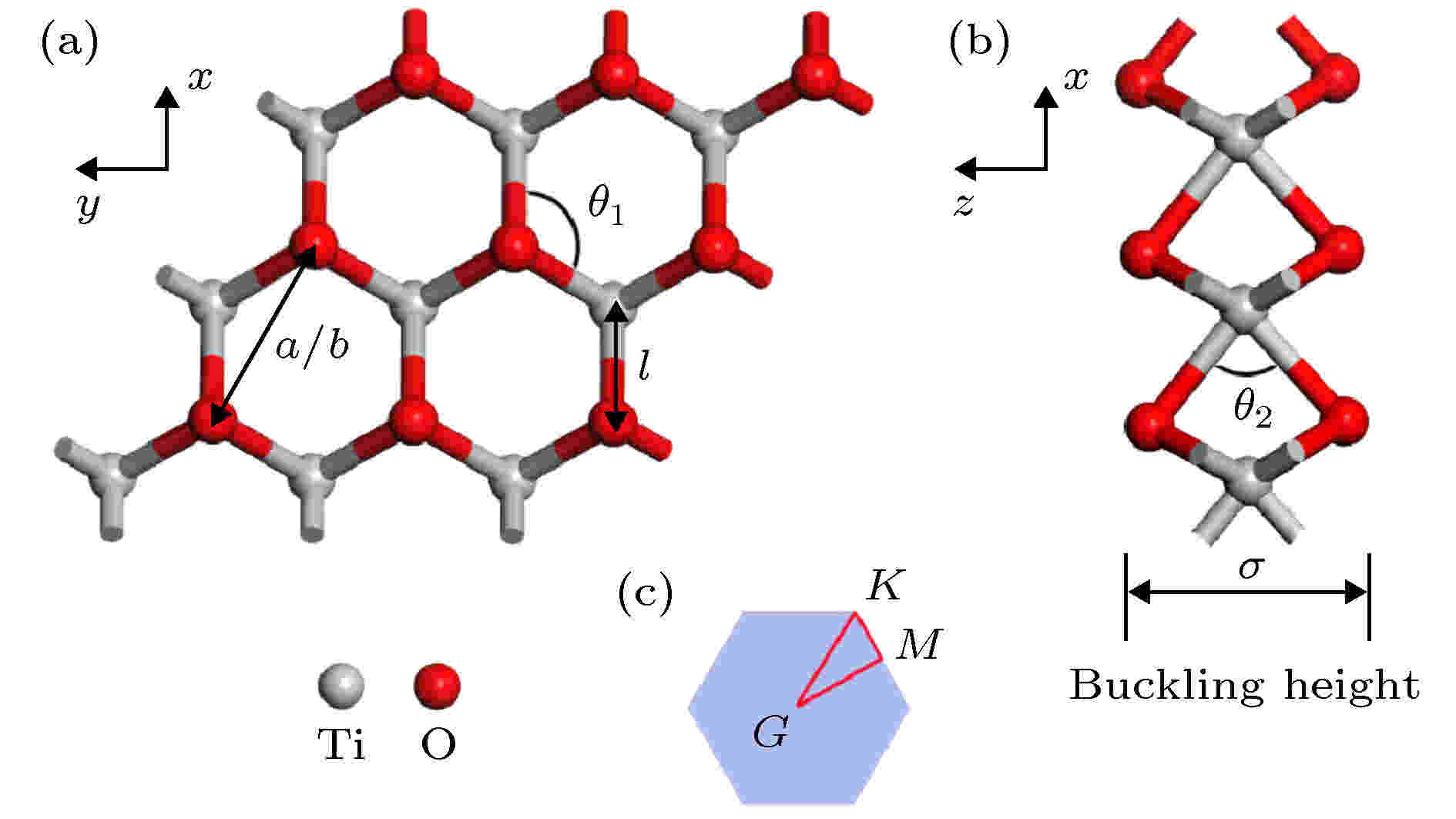
By means of state-of-the-art density functional theory (DFT) computations, We designed a new two-dimensional material TiO2. We further investigated the stability, electronic structure, carrier mobility, and optical properties of monolayer TiO2. Our results show that monolayer TiO2 has good kinetic, thermodynamic and mechanical stability and can exist stably at room temperature. The results were demonstrated using the binding energy, phonon spectrum, molecular dynamics simulation, and elastic constant calculation. The band structure indicates that the monolayer TiO2 is an indirect bandgap semiconductor with energy gaps of 1.19 eV (GGA+PBE) and 2.76 eV (HSE06), respectively. The results of state density show that the Ti-3d state electrons constitute the top of the valence band and Ti-4s state electrons constitute the bottom of the conduction band. The electron states of O atoms contribute very little near the Fermi energy level and are mainly distributed in the deep energy level. In addition, the carrier mobility of monolayer TiO2 is smaller than monolayer MoS2, and the electron and hole mobility can reach 31.09 cm2·V–1·s–1 and 36.29 cm2·V–1·s–1, respectively. Due to the anisotropy of hole mobility and electron mobility, the composite rate of electrons and holes is relatively low. This ensures longer service life and better photocatalytic activity of monolayer TiO2. Furthermore, under the condition of uniaxial strain and biaxial strain, the energy gap of monolayer TiO2 has a clear response. The energy gap is more sensitive to biaxial strain than uniaxial strain, indicating that monolayer TiO2 can be applied to various semiconductor devices. The band-edge potential and optical properties of semiconductors indicate that two-dimensional TiO2 is capable of photo-splitting water production, H2 at –5~2% single/biaxial strain, and O2, H2O2, O3, etc. at –5~5% single/biaxial strain. Moreover, the monolayer TiO2 has a high absorption coefficient for visible and ultraviolet light. In conclusion, the monolayer TiO2 has a potential application prospect in the field of optoelectronic devices and photocatalytic materials in the future.
CONDENSED MATTER: ELECTRONIC STRUCTURE, ELECTRICAL, MAGNETIC, AND OPTICAL PROPERTIES

2020, 69 (16): 167101.
doi: 10.7498/aps.69.20191930
Abstract +
OLEDs are popular as display technology nowadays, which have been widely used in commercial application. However, there are still some problems that blue light devices are not as efficient or stable as red and green light devices. Although the use of phosphorescent dyes can significantly improve the internal quantum efficiency, the high production cost and unstable performance limit the industrialization of phosphorescent OLEDs. In the development of OLEDs, the researchers found that OLEDs suffered from a decline in their efficiency at high brightness levels, a behavior known as “efficiency roll-off”. The efficiency roll-off is more pronounced in phosphorescent devices due to the longer lifetime of triplet exciton than singlet exciton, so that it has been widely investigated in recent years. Little is known, still, about fluorescent devices. Accordingly, unraveling the exciton loss mechanism in blue fluorescent OLEDs is particularly important, as it is a limiting factor for the improvement of efficiency. In this work, the efficiency roll-off in blue fluorescent OLEDs is investigated by observing the quenching of DPAVBI excitons. Firstly, the effects of electron current and hole current on photoluminescence(PL) behavior of unipolar devices are studied by steady-state and transient-state measurements, and we analyze PL spectrum and calculate the exciton quenching rate constant according to the transient PL decay curves to clarify the exciton quenching dynamics. The results show that the holes are much more efficient in quenching the excitons when the host is a hole transport material. This is different from the general understanding that exciton-polaron quenching effect with higher carrier mobility is weaker. Because the existence of bound charges produces additional charge density, and it is inferred that the exciton is mainly quenched by trapped charge rather than moving charge. We also exclude the effect of exciton–exciton annihilation and electric-field-induced dissociation on the efficiency degradation of the OLEDs. It is confirmed experimentally that exciton-polaron interaction is the dominant mechanism of the efficiency roll-off in fluorescent OLEDs. We then fabricate organic light-emitting diode devices with different doping concentrations to figure out the effect of doping concentration on exciton-polaron interaction, and obtain a blue fluorescence device with good comprehensive performance. We also summarize some feasible methods to optimize the efficiency of the OLEDs. In this paper, our findings about exciton-polaron interaction might provide a viable source for efficiency improvement by regulating charge trapping in light emitting layer.
COVER ARTICLE
2020, 69 (16): 167102.
doi: 10.7498/aps.69.20200646
Abstract +
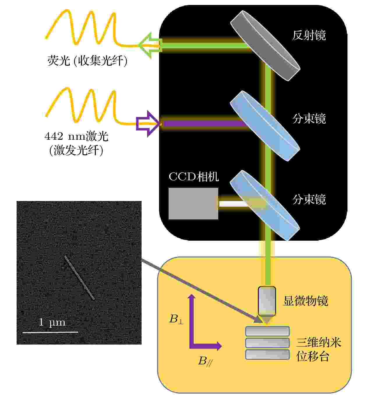
Hybrid organic-inorganic perovskites show large potential applications in solar cells, light emitting diodes and low threshold lasers because of the high tolerance of defects compared with other semiconductor materials. Normally they have been synthesized by dilution method, generating a device with high performance, but they also introduce lots of defects. So far, investigations have been done intensively on ensemble defects both in theory and experiment, but single-defect related trapped excitons are yet to be explored. In this work, we prepared high-quality CH3NH3PbBr3 perovskite nanowires with the length of about 1 μm and the width of several hundred nanometers by “reverse” ligand assisted reprecipitation method, and performed the magneto-photoluminescence measurement of different trapped excitons in single perovskite nanowires at a low temperature with a standard confocal microscopic system. The photoluminescence (PL) peak with narrow linewidth has been observed from trapped excitons with high luminescence intensity and the trapped excitons can be coupled with phonons in different ways. Both Zeeman splittings and diamagnetic effects have been observed in single trapped excitons under the magnetic field, and we found that the different trapped excitons have different Zeeman splittings and diamagnetic effects which is caused by the different defects near the trapped excitons. At the same time, we have extracted the g-factor of the trapped excitons under different magnetic field angles. The extracted exciton g-factors show anisotropic, which can be ascribed to the limitation of the lattice structure of the perovskite and the trapped exciton wave-function anisotropy under a vector magnetic field. Our results demonstrate that trapped excitons with narrow linewidth have very good luminescence properties and studying the magneto-optical properties from single trapped excitons can provide a deep understanding of trapped excitons in perovskites for applications in quantum light sources and spintronics. Furthermore, our results can also provide a possibility to control the electron spin in single-trapped-excitons-based hybrid organic-inorganic perovskites by manipulating the g-factor through an applied vector magnetic field, which promotes the application of the perovskite-based spintronics.

2020, 69 (16): 167301.
doi: 10.7498/aps.69.20200405
Abstract +
In order to enhance the working performance of existing temperature sensor and refractive index sensor of sub-wavelength waveguide, the design of ring regular octagon surface plasmon resonance sensor with sharp transmission peak, high sensitivity and high integration was proposed in this paper based on surface plasmon polaritons. The feasibility of using ethanol as a thermosensitive filler to establish a linear conversion relationship between temperature and effective refractive index was analyzed theoretically. The reason why the real part of effective refractive index changes abruptly with the change of waveguide width is also explained. The multimode interference coupled mode theory (MICMT) was used to fit and analyze the transmission peak of the sensor, and then the finite element methods (FEM) is used for simulation analysis. Results obtained by the theory of the MICMT are consistent very well with those from simulation. In order to obtain the optimal parameter setting of the ring regular octagon surface plasmon resonance sensor, various parameters of the sensor are simulated by FEM. It is found that increasing L and decreasing H will improve the sensitivity of the sensor, while decreasing parameter w can not only improve the amplitude of transmission peak, but also keep the sensitivity unchanged. This characteristic of parameter w greatly improves the robustness of the sensor. All kinds of physical phenomena in this paper are analyzed in detail. Firstly, the phenomenon of transmission peak displacement caused by parameter changes is explained through the analysis of magnetic field distribution, and then the phenomenon of inconsistent sensitivity of different transmission peaks is explained through photon energy formula. Compared with the previous structural design, the dual-purpose sensor has many advantages such as wide operating wavelength range, narrow full width at half maximum and easy to integrate. As a temperature sensor and refractive index sensor, its sensitivity was as high as 0.9 nm/℃ and 2400 nm/RIU. The study of this structure broke through the limitations of some traditional cavities, in order to provide a high- performance cavity selection for the micro-nano photon temperature and refractive index dual-purpose sensor based on the design of surface plasmon polaritons in the future.
2020, 69 (16): 167801.
doi: 10.7498/aps.69.20200457
Abstract +
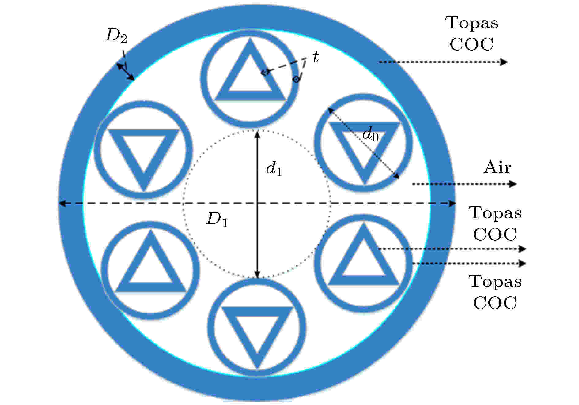
In the terahertz communication and imaging systems, terahertz fibers have aroused great interest in the past several years. Countering the terahertz wave applications ‘inefficient transmission’ calls for a rapid development in terahertz fibers that could achieve low confinement loss, chromatic dispersion and large refraction of power at the same time. In this paper, a new type of negative curvature terahertz fiber is designed, which consists of six cladding tubes evenly distributed in the cladding and nested with equilateral triangle structure. By using full vector finite element method and changing the thickness of cladding tube and triangle, the effective mode field area, core power ratio, confinement loss, dispersion and other parameters of negative curvature fiber are studied. Here, the thickness range of 70–100 μm is selected. It is found that the confinement loss of optical fiber can reach 0.005 dB/cm at 2.36 THz, the dispersion coefficient can float up and down at ±0.1 ps/(THz·cm) at the frequency range of 2.1–2.8 THz, the core power ratio can reach above 99% in the same frequency range. Compared with the known terahertz negative curvature fiber, the nested triangle negative curvature fiber has lower confinement loss and wide transmission bandwidth of 2.1–2.8 THz. After that, when the cladding tube and the triangle thickness are kept at 90 μm, the bending degree of the triangle edge is changed, and the above properties are further studied. When the triangle edge is bent in and out, the transmission performance of the fiber is analyzed. It is found that when the triangle edge is bent inward, the transmission characteristics of terahertz wave is much better than that when the triangle edge is bent outward. When the triangle edge is bent inwards, the confinement loss is obviously reduced, reaching 0.002 dB/cm at 2.36 THz. Compared with triangle straight edge, the confinement loss is reduced by 40% and still maintaining 99% core power ratio at certain frequency band. The designed terahertz fiber will have an important application value in the fields of sensing and imaging systems with low loss and wide bandwidth. This makes the Topas COC-based terahertz fiber very suitable for guiding terahertz wave over the desired frequency range.
2020, 69 (16): 167802.
doi: 10.7498/aps.69.20200269
Abstract +
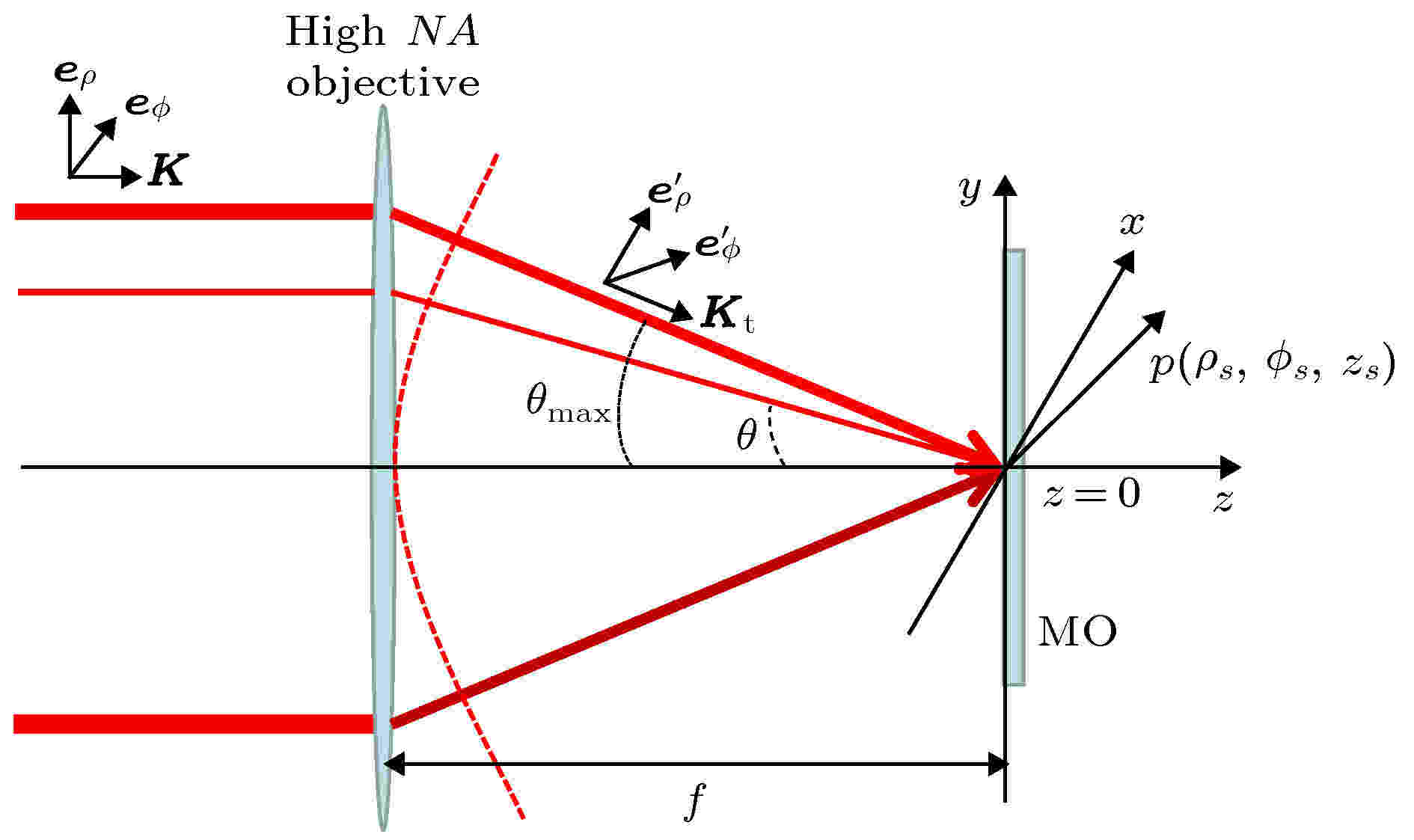
All-optical magnetic recording based on the inverse Faraday effect has become a research hotspot in recent years due to its ultra-high storage density and ultra-fast magnetization reversal rate. Existing studies have shown that by optimizing the phase modulation or performing 4π tight focusing of azimuthally polarized vortex beams, high-resolution longitudinal magnetization fields with different axisymmetric intensity patterns can be generated. In order to meet the requirements of more complex all-optical magnetic recording and asymmetric magnetic particle capture and manipulation, it is particularly important to generate an asymmetric light-induced magnetization field with adjustable center position. Studies have shown that the fractional vortex phase could lead to the asymmetric focal field distribution generation under tight focusing conditions, which means that the tightly-focused azimuthally polarized light carrying the fractional vortex phase can produce a novel asymmetric light-induced magnetization field. As a new degree of freedom for the regulation of the magnetization field, the fractional topological charge will bring more new phenomena, new effects and new applications in the field of interaction between light and matter. In this work, for the first time to our knowledge, the magnetization induced by tightly focused azimuthally polarized fractional vortex beam is studied based on the Richard-Wolf vector diffraction theory and the inverse Faraday effect. The equivalent approximation of the magnetization induced by azimuthally polarized fractional vortex beam regarded as a weighted superposition of magnetization induced and crossly induced by a finite number of azimuthally polarized adjacent integer-order vortex beams, where the number of the equivalent terms is chosen by using the histogram intersection method of the intensity distribution image of the magnetization field. The magnetization field distribution under different values of α are also numerically simulated. Studies have shown that magnetization induced by the azimuthally polarized fractional vortex beam is asymmetrically distributed. When the fractional vortex topological charge α belongs to [0.5,1.5], as the vortex topological load increases, the splitting phenomenon of the transverse distribution of magnetization field appears with the magnetization spot position shift in the direction perpendicular to the optical axis. When α equals 0.5 or 1.5, the maximum offset of the center of the magnetization spot is 0.24λ. When the fractional vortex topological charge α belongs to [2,3], the transverse distribution of magnetization field splits two hot intensity spots with gradually growing outer ring diameter. When the fractional vortex topological charge α tends to be an integer 3, the transverse distribution of magnetization field also gets round and symmetrical. In particular, when the fractional vortex topological charge α is a half-integer, especially larger than 3. The number of hot spots ($\alpha - 0.5 $ ) of the intensity of the magnetization field and the number of dark spots ($ \alpha - 1.5 $ ) surrounded by them all have a positive correlation with the number of vortex order. The research in this paper is expected to have new applications in the fields of all-optical magnetic recording and the capture and manipulation of magnetic particles.

EDITOR'S SUGGESTION
2020, 69 (16): 167803.
doi: 10.7498/aps.69.20200696
Abstract +
Black phosphorus (BP) has been attracting intense interest due to its unique anisotropic properties. The investigations on phonon dispersion and electronic band structure could expand the understanding of the properties of BP and promote its application on next generation nano-electronic devices. As the fingerprint of materials, Raman spectroscopy can provide the information of their phonon dispersion and electronic band structure. According to the Raman selection rule, Raman process involving multiple (two or more) phonons can be used to probe the phonon density of states within the whole Brillouin zone. However, the intensity of high-order Raman modes is much lower than that of the first-order Raman mode. To break through the limit of low intensity, here, we measured the resonant Raman spectroscopy of BP excited by several wavelength lasers and observed rich information about high-order Raman modes in the spectral range of 680–930 cm–1. To further investigate high-order Raman modes and avoid the birefringence effects from optical anisotropy on Raman intensity, we employ a special polarization configuration to obtain resonant Raman spectra and Raman intensity as a function of excitation wavelength. All the observed high-order Raman modes are certainly assigned, according to the phonon dispersion and symmetry analysis of related phonons. This indicates the great contribution of phonons within the Brillouin zone to the second- and third-order Raman scattering. This work proposes a general and systematical method to investigate high-order Raman modes, and paves ways for the researches of phonon dispersion and resonance Raman spectroscopy in other anisotropic materials.
2020, 69 (16): 167805.
doi: 10.7498/aps.69.20200445
Abstract +
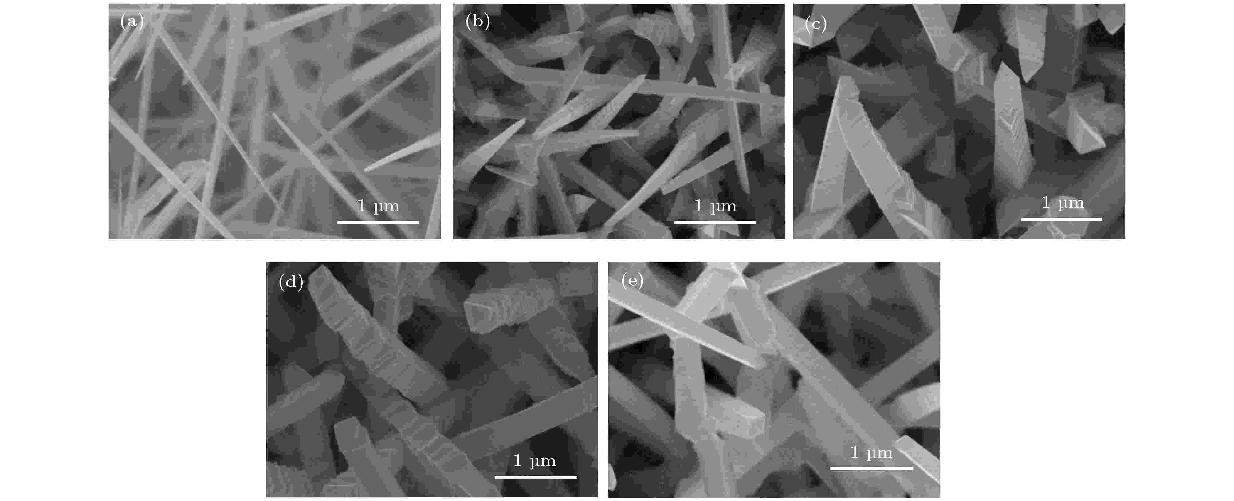
GaN nanomaterials, as one of the most important third-generation semiconductor materials, have attracted wide attention. In this study, GaN nanowires with square cross section were successfully prepared by microwave plasma chemical vapor deposition system. The diameters of nanowires are from 300 to 500 nm and the lengths from 15 to 20 μm. The results show that the cross section of nanowires could be transformed from triangle into square by adjusting the ratio of Mg to Ga in source materials. X-ray diffraction(XRD)result indicate that the structure of GaN nanowires are agree with the hexagonal wurtzite. X-ray photoelectron spectroscopy (XPS) rusult show that a certain amount of Mg and O impurities incoporated in the square-shaped GaN nanowires. Transmission electron microscopy (TEM) result suggested that square-shaped GaN nanowires had high crystallinity with a growth direction of [$0\bar 110$ ]. The ratio of source materials- and time-depented growth mechanism was also studied. It was suggested that the transformation of the cross section from triangle to square structure should be derived from the growth mechanism change from vapor-liquid-solid(VLS)process to vapor-solid(VS)process. The doped Mg increased the growth rate of the nanowires sidewalls, which led to a symmetrically growth of GaN nanowires along the twin boundaries. GaN nanowires gradually transformed to square structure by auto-catalytic growth. Moreover, the property of field emission were further investigated. The results showed that the turn-on electric field of square-shaped GaN nanowires was 5.2 V/m and a stable field emission property at high electric field. This research provides a new method for the preparation of square-shaped GaN nanowires and a prospective way for the design and fabrication of novel nano-scale devices.
INTERDISCIPLINARY PHYSICS AND RELATED AREAS OF SCIENCE AND TECHNOLOGY

EDITOR'S SUGGESTION
2020, 69 (16): 168101.
doi: 10.7498/aps.69.20200481
Abstract +

2020, 69 (16): 168201.
doi: 10.7498/aps.69.20200411
Abstract +

2020, 69 (16): 168202.
doi: 10.7498/aps.69.20200074
Abstract +
Manipulating a single DNA molecule and effectively introducing it into and exporting micro-nano-fluidic channels are prerequisites for the functional DNA biochips. And it is the key to the precise separation and screening of different DNA molecules by the micro-/nanochannel system that accurately understanding the movement characteristics and dynamic mechanism of DNA molecules moving near the channel port. In this paper, the electrodynamic characteristics of λ-DNA molecule entering into/leaving off a 50 μm channel port driven by the electric field force are systematically investigated and analyzed by the single molecule fluorescence microscopy. The experimental results indicated that there were the maximum (Emax) and minimum (Emin) thresholds of the applied electric field intensity, and only when the field intensity E meets Emin ≤ E ≤ Emax, the single λ-DNA molecule could successfully enter into the trans port and exit out of the cis port; when the electric field intensity was less than the minimum threshold, E ≤ Emin, λ-DNA molecules could not enter the trans port; when the electric field intensity was greater than the maximum threshold, Emax ≤ E, λ-DNA molecules could move into the microchannel through the trans port, but not exit out of the cis port. When λ-DNA molecule migrated toward the cis port along the channel, the movement state was changed, some new phenomena were observed, e.g. the translocation direction was reversed, reciprocated, or even rotated; moreover, the DNA molecules were easy to adhere to the channel wall. In addition, when the electric field intensity enhanced, the distance between the position where DNA molecular direction reversing and the cis port was increased. Based on the microfluidic electrodynamics, the physical mechanism of the velocities and translocation states of single λ-DNA molecule passing microchannel port was preliminarily analyzed. The results of this study have certain practical guiding significance for the development of gene chip laboratory and DNA molecular sensors based on the micro/nanochannel fluidic system.
2020, 69 (16): 168701.
doi: 10.7498/aps.69.20200397
Abstract +
Gallium nitride (GaN) is a key material in blue light-emitting devices and is recognized as one of the most important semiconductors after Si. Its outstanding thermal conductivity, high saturation velocity, and high breakdown electric field have enabled the use of GaN for high-power and high-frequency devices. Although lots of researches have been done on the optical and optoelectrical properties of GaN, the defect-related ultrafast dynamics of the photo-excitation and the relaxation mechanism are still completely unclear at present, especially when the photo-generated carrier concentration is close to the defect density in n-type GaN. The transient absorption spectroscopy has become a powerful spectroscopic method, and the advantages of this method are contact-free, highly sensitive to free carriers, and femtosecond time resolved. In this article, by employing optical pump and infrared probe spectroscopy, we investigate the ultrafast photo-generated carriers dynamics in representative high-purity n-type and Ge-doped GaN (GaN:Ge) crystal. The transient absorption response increased as probe wavelengths increased, and hole-related absorption was superior to electron-related absorption, especially at 1050 nm. The transient absorption kinetics in GaN:Ge appeared to be double exponential decay under two-photon excitation. By modelling the carrier population dynamics in energy levels, which contained both radiative and non-radiative defect states, the carrier dynamics and carrier capture coefficients in GaN: Ge can be interpreted and determined unambiguously. The faster component (30–60 ps) of absorption decay kinetics corresponded to the capturing process of holes by negatively charged acceptor CN. However, the capturing process was limited by the recombination of electron and trapped holes under higher excitation after the saturation of deep acceptors. As a result, the slower component decayed slower as the excitation fluence increased. Moreover, the experimental and theoretical results found that, the carrier lifetime in n-GaN can be modulated by controlling the defect density and carrier concentration under a moderate carrier injection, making GaN applicable in different fields such as LED and optical communication.

2020, 69 (16): 168702.
doi: 10.7498/aps.69.20200171
Abstract +
Optical microscopy has the advantages of real-time, non-invasive, tomography, three-dimensional imaging and living imaging. However, its spatial resolution cannot exceed half wavelength due to the existence of optical diffraction limit, which limits the development of optical microscopy. The primary task of super-resolution imaging is to break the diffraction limit and improve the resolution of optical microscopy for study of subcellular structure. Many kinds of super-resolution imaging technologies have been reported, among which the stimulated emission depletion (STED) microscopy is the earliest imaging technology to break the optical diffraction limit at present. STED microscopy can achieve nanometer-scale spatial resolution by breaking the optical diffraction limit with pure optical methods and a clever optical design. However, the application of STED microscopy in biomedicine, especially in live cell imaging is limited by high illumination power of STED light. In this paper, a new type of STED probe has been developed. The spectral analysis results show that the peak of the excitation and emission spectrum of this probe is as far as 122 nm away from each other, which is very suitable for the study of STED super-resolution because of its long stokes redshift. After colocalization with commercial mitochondrial dyes, it was found that the probe had a higher localization coefficient with commercial dyes and could be well positioned on mitochondrial organelles. At the same time, it was found that strong mitochondrial signal could be detected with low-power excitation light (only 1 μW in the experiment), and can get higher resolution of 62 nm under the STED light with 39.5 mW. The result of measuring the transverse resolution obtained by STED light under different power shows that the saturated light power of the probe is 3.5 mW (1.1 MW·cm–2). Through the anti-bleaching testing, the probe still has a strong fluorescence intensity after more than 300 times of high power light irradiation, which indicates that the probe has a strong anti-bleaching property. Through a series of tests, this paper present a novel STED probe which has good mitochondrial targeting, excellent photobleaching-resistance, high resolution and low saturation power, which provides a new research tool for long-term live cell mitochondrial super-resolution imaging.

2020, 69 (16): 168703.
doi: 10.7498/aps.69.20200554
Abstract +
Fluorescence lifetime imaging microscopy (FLIM) is widely used in biomedical, materials and other fields. It not only has strong specificity and high sensitivity, but also has the capability of quantitative measurement because the fluorescence lifetime is not affected by the intensity of excitation, the concentration of fluorophores and photobleaching, and consequently is able to monitor the changes of microenvironment and reflecting the interaction between molecules. However, its application is limited to some extent by the complexity of data analysis. In order to make FLIM technology more suitable for fast analysis of high-throughput data, a variety of new algorithms for fluorescence lifetime analysis have emerged in recent years, such as phasor analysis, maximum likelihood estimation, first-order moment, Bayesian analysis, and compressed sensing. Among them, the phasor analysis (PA) method obtains the fluorescence lifetime by converting the fitting in the time domain to the direct calculation in the frequency domain. Compared with traditional least-square fitting method, it is not only simpler and faster, but also more suitable for the case of low photon counts. In addition, in the PA approach to FLIM, the fluorescence decay is directly converted into a phasor diagram by simple mathematics, where the phasor points originating from different pixels in the image are represented by the positions in the phasor plot, and thus the graphical representation obtained by PA method is convenient for data visualization and cluster analysis. Therefore, it has become a simple and powerful analysis method for FLIM, and is increasingly favored by researchers. In this paper, the basic principle of PA method and how we can use it are described in detail. And on this basis, the latest application research progress of the method in cell metabolism state measurement, protein interaction study, cell microenvironment measurement, auxiliary pathological diagnosis, and resolution improvement in super-resolution imaging are introduced and summarized. The advantages of PA method in these FLIM applications are focused on, providing useful reference for the research in related fields. Finally, the phasor analysis method for FLIM data analysis and the development trend of its application are prospected.

2020, 69 (16): 168901.
doi: 10.7498/aps.69.20191162
Abstract +
Link prediction is an important issue in network analysis tasks, which aims at detecting missing, spurious or evolving links in a network, based on the topology information of the network and/or the attributes of the nodes. It has been applied to many real-world applications, such as information integration, social network analysis, recommendation systems, and bioinformatics. Existing link prediction methods focus on static networks and ignore the transmission of dynamic information in the network. However, many graphs in practical applications are dynamic and evolve constantly over time. How to capture time information in a dynamic network and improve the accuracy of link prediction remains a conspicuous challenge. To tackle these challenges, we propose a dynamic network representation based link prediction model, named DNRLP. DNRLP can be mainly divided into two modules: a representation learning module on dynamic network and a link prediction module, where the representation learning module is composed of a node information dynamic update unit and a node neighborhood update unit. Node information dynamic update unit leverages the benefits of the long short-term memory (LSTM) in capturing time information and uses a Time Interval based Filter Unit (TIFU) to introduce time interval information between two links, while for the node neighborhood update unit we present a random walk algorithm based on connection strength to simulate the diffusion of dynamic information. Through the above two parts, the model can obtain the node representation at the new moment, then link prediction is performed by the link prediction module by measuring the similarity between the node representations. The experiment uses MRR and Recall@k indicators to evaluate performance of model on four public dynamic network datasets. The experiments demonstrate the effectiveness and the credibility of the proposed model in link prediction tasks as compared with the comparison models, the MNR index of the DNRLP is increased by 30.8%. The model proposed in this paper not only learns the dynamic information in the network, but also considers its influence on neighbors and the impact of time interval on information update. Therefore, the model has learned more abundant dynamic information and has obvious advantages for link prediction tasks.
GEOPHYSICS, ASTRONOMY, AND ASTROPHYSICS

2020, 69 (16): 169601.
doi: 10.7498/aps.69.20200041
Abstract +
In this paper, we investigated 82 type-II radio burst events detected by some ground stations Learmonth, YNAO, and BIRS and spacecraft Wind/WAVES, STEREO/WAVES from January 2007 to December 2015. And we identified 39 events associated with radio enhancement and 43 events without enhancement. We found that: 1) The CME velocity, mass, kinetic energy and flare class with respect to type II radio enhancement events were generally higher than that of no enhancement events, and these properties in the solar energetic particle (SEP) events were significantly higher than that no SEP event, regardless of whether radio enhancement or not. 2) As shown in the characteristic time analysis, the initial release time of SEPs is generally earlier than the start time of radio enhancement, so we can the radio enhancement is only as a signature of the shock enhancement rather than the direct generator of SEP events. 3) Whether radio enhancement or not, the onset height of type IIs associated with SEP event is slightly lower than that of event without SEP. For the absence height, the SEP events are significantly higher than the no-SEP events, and that the absence height of enhancement events are also distinctly higher than that non-enhancement events, which reveals that the enhanced CME shock characterized by enhanced radio burst can keep propagating to more higher or further space. 4) When one fast and wide CME fully sweeps over another slow and narrow preceding CME, CME interaction can more easily generate radio enhancement, but no distinctive difference between SEP events and non-SEP events. So the results of this paper reveal that radio enhancement can be regarded as a manifestation of CME shock becoming strong during interacting with other CME, and the enhanced shock can accelerate the particle to generate large SEP events more easily. However, the type II radio enhancement is not the direct producer or causer that generate large SEP event.


