


-
Amorphous indium gallium zinc oxide (IGZO) thin film transistors (TFT) are widely used in active-matrix displays because of their excellent stability, low off-current, high field-effect mobility, and good process compatibility. Among IGZO TFT device structures, back channel etching (BCE) is favorable due to low production cost, short channel length and small SD-to-gate capacitance. In this work, prepared are the BCE IGZO TFTs each with the passivation layer of silicon dioxide (SiO2), polyimide (PI) or SiO2-PI stacked structure to study their difference in back channel hydrogen impurity and diffusion behavior. Comparing with the conventional SiO2 passivation BCE TFT, the performance of PI passivation TFT is improved greatly, specifically, the saturation field effect mobility increases from 4.7 to 22.4 cm2/(V·s), subthreshold swing decreases from 1.6 to 0.28 V/decade, and the an on-off current ratio rises dramatically from 1.1×10⁷ to 1.5×10¹⁰. After the SiO2 passivation layer is substituted with PI, the I off decreases from 10–11 A to 10–14 A, which indicates that there exist less shallow-level donor states of hydrogen impurities, which might be explained by the following three mechanisms: first, in the film formation process of PI, the direct incorporation of hydrogen-related radicals from SiH4 precursor into the back channel is avoided; second, the hydrogen content in the PI film is lower and harder to diffuse into the back channel; third, the hydrogen impurity of back channel that is introduced by the H2O2-based etchant in the SD etching process could diffuse more easily toward the PI layer. The TFTs with PI passivation layer also shows the less electrical degradation after the annealing treatment at 380 ℃ and better output performance, which confirms less defects and higher quality of the back channel. The bias stabilities of PI devices are improved comprehensively, especially negative bias illumination stability with the threshold voltage shifting from –4.8 V to –0.7 V, which might be attributed to the disappearance of hydrogen interstitial sites and hydrogen vacancies that are charged positively in the back channel. The PI passivation layer is effective to avoid back channel hydrogen impurities of BCE TFT and promises to have broad applications in the display industry.
[1] 朱乐永, 高娅娜, 张建华, 李喜峰 2015 物理学报 64 108501
 Google Scholar
Zhu L Y, Gao Y N, Zhang J H, Li X F J 2015 Acta Phys. Sin. 64 108501
Google Scholar
[2] He P, Hong R, Li G, Zou X, Hu W, Lan L, Iñíguez B, Liao L, Liu X J 2022 IEEE Trans. Electron Devices 43 1894
Google Scholar
[3] Kwon J Y, Lee D J, Kim K B 2011 Electron. Mater. Lett. 7 1
Google Scholar
[4] Kang D H, Kang I, Ryu S H, Jang J 2011 IEEE Electron Device Lett. 32 1385
Google Scholar
[5] Bonneville D B, Miller J W, Smyth C, Mascher P, Bradley J D 2021 Appl. Sci. 11 2110
Google Scholar
[6] Chowdhury M D H, Mativenga M, Um J G, Mruthyunjaya R K, Heiler G N, Tredwell T J, Jang J 2015 IEEE Trans. Electron Devices 62 869
Google Scholar
[7] Jeong S G, Jeong H J, Choi W H, Kim K, Park J S 2020 IEEE Trans. Electron Devices 67 4250
Google Scholar
[8] LI G, YANG B-R, LIU C, Lee C Y, Tseng C Y, Lo C C, Xu N 2015 J. Phys. D. 48 475107
Google Scholar
[9] 郭海泉, 杨正华, 高连勋 2021 应用化学 38 1119
Google Scholar
Guo H Q, Yang Z H, Gao L X 2021 Chinese J. Appl. Chem. 38 1119
Google Scholar
[10] Sezer H A, Celik B A 2021 SN Appl. Sci. 1 22
Google Scholar
[11] Nakata M, Ochi M, Tsuji H, Takei T, Miyakawa M, Yamamoto T, Fujisaki Y 2019 J. Appl. Phys. 58 090602
Google Scholar
[12] Xu H, Lan L, Xu M, Zou J, Wang L, Wang D, Peng J High 2011 Appl. Phys. Lett. 99 253501
Google Scholar
[13] Ide K, Nomura K, Hosono H, Kamiya T 2019 Phys. Status Solidi 216 1800372
Google Scholar
[14] Hanyu Y, Domen K, Nomura K, Hiramatsu H, Kumomi H, Hosono H, Kamiya T 2013 Appl. Phys. Lett. 103 202114
Google Scholar
[15] Li M, Huang D, Li M, Zhang W, Xu H, Zou J, Xu M 2019 IEEE Trans. Electron Devices 66 3854
Google Scholar
[16] Han K L, Cho H S, Ok K C, Oh S, Park J S 2018 Electron. Mater. Lett. 14 749
Google Scholar
[17] Flack W W, Flores G E, Christensen L D H, Newman G 1996 Optical Microlithography IX. SPIE (Santa Clara CA)p169
[18] 邵龑, 丁士进 2018 物理学报 67 098502
Google Scholar
Shao Y, Ding S J 2018 Acta Phys. Sin. 67 098502
Google Scholar
[19] Kang Y, Ahn B D, Song J H, Mo Y G, Nahm H H, Han S, Jeong J K 2015 Adv. Electron. Mater. 1 1400006
Google Scholar
[20] Noh H K, Park J S, Chang K J 2013 J. Appl. Phys. 113 063712
Google Scholar
[21] Choi S H, Jang J H, Kim J J, Han M K 2012 IEEE Electron Device Lett. 33 381
Google Scholar
[22] Nomura K, Kamiya T, Hosono H 2012 ECS J. Solid State Sci. Technol. 2 5
Google Scholar
-
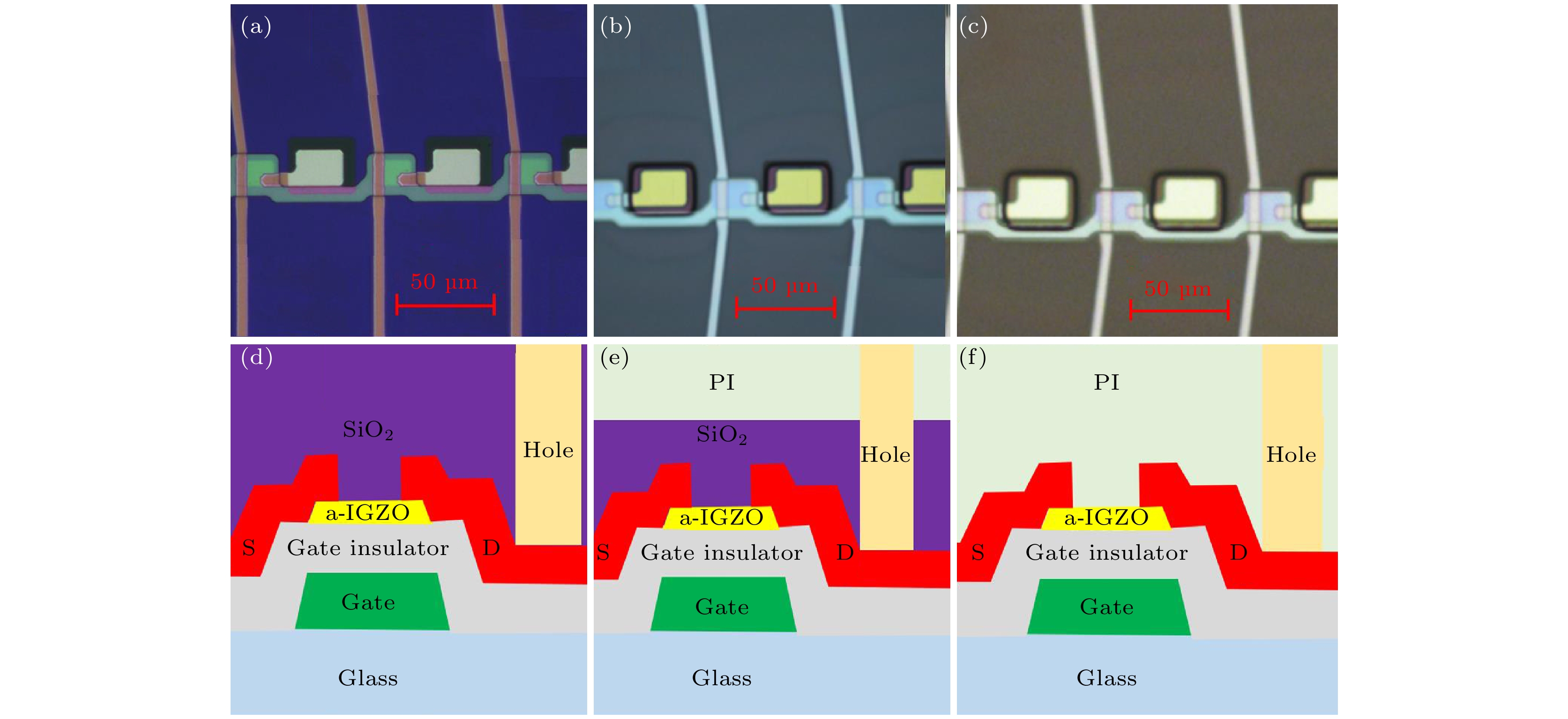
图 1 SiO2钝化层(a)、SiO2-PI钝化层(b)、PI钝化层(c)BCE TFT的阵列的光学显微镜俯视图; SiO2钝化层(d)、SiO2-PI钝化层(e)、PI钝化层(f)BCE TFT的器件结构示意图
Fig. 1. Top view of the array of BCE TFT with the passivation layer of SiO2 (a), SiO2-PI (b) and PI (c) taken by optical microscopy; schematic diagram of the BCE TFT with the passivation layer of SiO2 (d), SiO2-PI (e) and PI (f).

图 2 SiO2钝化层(a)、SiO2-PI钝化层(c)、PI钝化层(e)BCE TFT制备后的与380 ℃退火后的转移特性; SiO2钝化层(b)、SiO2-PI钝化层(d)、PI钝化层(f)BCE TFT在5.0 V, 7.5 V和10.0 V栅压下的输出特性
Fig. 2. Transfer characteristics of as-fabricated and 380 ℃-annealed BCE TFT with the passivation layer of SiO2 (a), SiO2-PI (c) and PI (e); output characteristics under the Vg of 5.0 V, 7.5 V or 10.0 V of BCE TFT with the passivation layer of SiO2 (b), SiO2-PI (d) and PI (f).

图 3 背沟道的X射线光子能谱(XPS)O 1s分峰图像(a); SiO2钝化层(b)、SiO2-PI钝化层(c)、PI钝化层(d)BCE TFT的背沟道化学动力学过程示意图
Fig. 3. Deconvoluted O 1s spectra of back channel (a); schematic diagrams of the chemical dynamic process of the back channel of BCE TFT with the passivation layer of SiO2 (b), SiO2-PI (c) and PI (d).
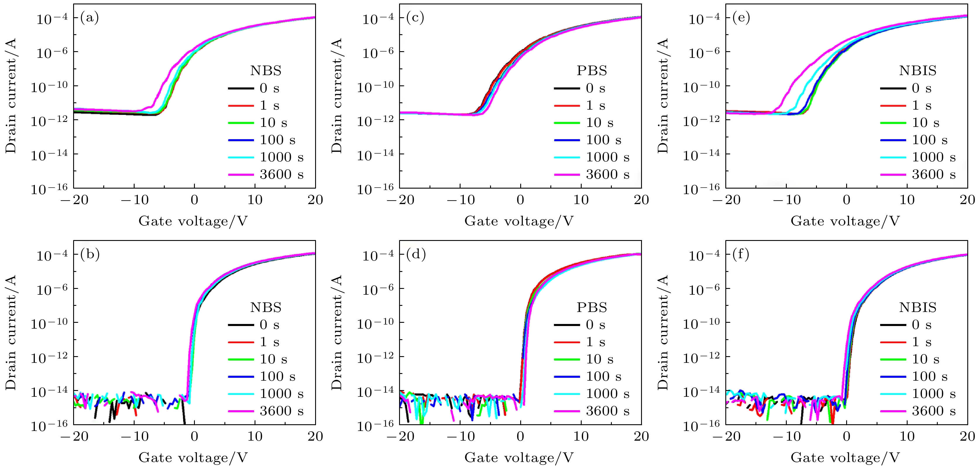
图 4 偏压稳定性, Vg = ±20 V, Vd = 0.1 V SiO2钝化层(a)或PI钝化层(b) BCE TFT的负偏压稳定性(NBS); SiO2钝化层(c)或PI钝化层(d) BCE TFT的正偏压稳定性(PBS); SiO2钝化层(e)或PI钝化层(f) BCE TFT的负偏压光照稳定性(NBIS)
Fig. 4. Bias stability, Vg = ±20 V, Vd = 0.1 V: NBS of BCE TFT with the passivation layer of SiO2 (a) and PI (b); PBS of BCE TFT with the passivation layer of SiO2 (c) and PI (d); NBIS of BCE TFT with the passivation layer of SiO2 (e) and PI (f).
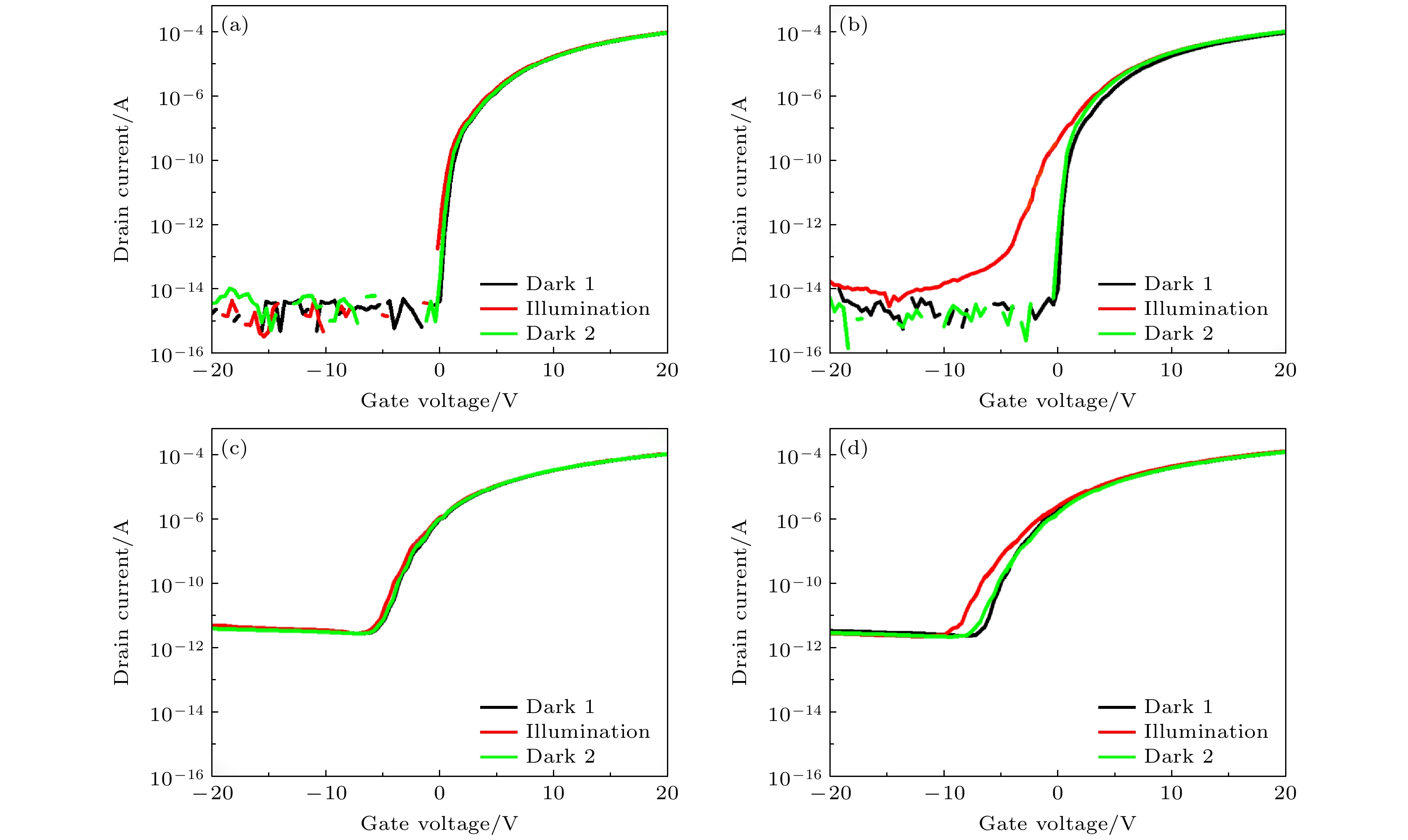
图 5 PI钝化层BCE TFT在底部光照(a)或顶部光照(b)下的转移特性退化; SiO2钝化层BCE TFT在底部光照(c)或顶部光照(d)下的转移特性退化
Fig. 5. Bottom illumination (a) and top illumination (b) induced degradation of transfer characteristics of BCE TFT with the passivation layer of PI; bottom illumination (c) and top illumination (d) induced degradation of transfer characteristics of BCE TFT with the passivation layer of SiO2.
-
[1] 朱乐永, 高娅娜, 张建华, 李喜峰 2015 物理学报 64 108501
Google Scholar
Zhu L Y, Gao Y N, Zhang J H, Li X F J 2015 Acta Phys. Sin. 64 108501
Google Scholar
[2] He P, Hong R, Li G, Zou X, Hu W, Lan L, Iñíguez B, Liao L, Liu X J 2022 IEEE Trans. Electron Devices 43 1894
Google Scholar
[3] Kwon J Y, Lee D J, Kim K B 2011 Electron. Mater. Lett. 7 1
Google Scholar
[4] Kang D H, Kang I, Ryu S H, Jang J 2011 IEEE Electron Device Lett. 32 1385
Google Scholar
[5] Bonneville D B, Miller J W, Smyth C, Mascher P, Bradley J D 2021 Appl. Sci. 11 2110
Google Scholar
[6] Chowdhury M D H, Mativenga M, Um J G, Mruthyunjaya R K, Heiler G N, Tredwell T J, Jang J 2015 IEEE Trans. Electron Devices 62 869
Google Scholar
[7] Jeong S G, Jeong H J, Choi W H, Kim K, Park J S 2020 IEEE Trans. Electron Devices 67 4250
Google Scholar
[8] LI G, YANG B-R, LIU C, Lee C Y, Tseng C Y, Lo C C, Xu N 2015 J. Phys. D. 48 475107
Google Scholar
[9] 郭海泉, 杨正华, 高连勋 2021 应用化学 38 1119
Google Scholar
Guo H Q, Yang Z H, Gao L X 2021 Chinese J. Appl. Chem. 38 1119
Google Scholar
[10] Sezer H A, Celik B A 2021 SN Appl. Sci. 1 22
Google Scholar
[11] Nakata M, Ochi M, Tsuji H, Takei T, Miyakawa M, Yamamoto T, Fujisaki Y 2019 J. Appl. Phys. 58 090602
Google Scholar
[12] Xu H, Lan L, Xu M, Zou J, Wang L, Wang D, Peng J High 2011 Appl. Phys. Lett. 99 253501
Google Scholar
[13] Ide K, Nomura K, Hosono H, Kamiya T 2019 Phys. Status Solidi 216 1800372
Google Scholar
[14] Hanyu Y, Domen K, Nomura K, Hiramatsu H, Kumomi H, Hosono H, Kamiya T 2013 Appl. Phys. Lett. 103 202114
Google Scholar
[15] Li M, Huang D, Li M, Zhang W, Xu H, Zou J, Xu M 2019 IEEE Trans. Electron Devices 66 3854
Google Scholar
[16] Han K L, Cho H S, Ok K C, Oh S, Park J S 2018 Electron. Mater. Lett. 14 749
Google Scholar
[17] Flack W W, Flores G E, Christensen L D H, Newman G 1996 Optical Microlithography IX. SPIE (Santa Clara CA)p169
[18] 邵龑, 丁士进 2018 物理学报 67 098502
Google Scholar
Shao Y, Ding S J 2018 Acta Phys. Sin. 67 098502
Google Scholar
[19] Kang Y, Ahn B D, Song J H, Mo Y G, Nahm H H, Han S, Jeong J K 2015 Adv. Electron. Mater. 1 1400006
Google Scholar
[20] Noh H K, Park J S, Chang K J 2013 J. Appl. Phys. 113 063712
Google Scholar
[21] Choi S H, Jang J H, Kim J J, Han M K 2012 IEEE Electron Device Lett. 33 381
Google Scholar
[22] Nomura K, Kamiya T, Hosono H 2012 ECS J. Solid State Sci. Technol. 2 5
Google Scholar

 下载:
下载:
计量
- 文章访问数: 5998
- PDF下载量: 133
- 被引次数: 0
