


-
BiFeO3作为一种具有体光伏效应的室温多铁材料, 是近年来多功能材料领域的研究热点. 其中磁、光、电等多种性能之间耦合作用的共存带来了丰富而复杂的物理内涵. 利用脉冲激光沉积在导电玻璃(SnO2:F, FTO)衬底上沉积了BiFeO3薄膜, 实验结果表明, 该薄膜具有良好的铁磁和铁电性能, 并通过磁场实现了对薄膜光电性能的调控. 在标准太阳光照的同时施加1.3 kOe (1 Oe = 103/(4π) A/m)磁场下, 磁-光电流变化率达到232.7%. BiFeO3薄膜中的磁-光电流效应来自于光磁电阻效应, 即光生电子在磁场作用下成为自旋光电子, 在材料导带运动过程中受到自旋相关散射而具有光磁电阻效应; 此外, 磁场作用使这些自旋光电子受到的畴壁散射减弱也进一步增强了磁光电流效应. 本文为磁场、光场调控多铁性薄膜的磁、光、电等物理特性提供了参考, 为多功能光电材料领域的器件研究与应用提供了基础.BiFeO3 (BFO) is a kind of room temperature multiferroic material with bulk photovoltaic effect, and it has been a research hotspot in the field of multifunctional materials in recent years. The coexistence of the coupling among magnetic, optical, electrical properties brings rich and complex physical connotations. In this work, BiFeO3 thin film is deposited on FTO substrate by pulsed laser deposition, and the solar cell structure with BiFeO3 film used as light absorption layer and Au film serving as electrode is constructed. X-ray diffraction and Raman spectra indicate that the BFO film grown on FTO substrate has a pure phase structure. The experimental results of physical properties indicate that the BFO film possesses good ferromagnetic and ferroelectric properties and obvious photoelectric effect. According to the hysteresis loop, the remanence (Mr) of the sample is 0.8 emu/cm3, and the coercivity (Hc) is 200 Oe at 300 K. In terms of ferroelectricity, the saturation polarization intensity of the sample can reach 0.997 μC/cm2, the residual polarization intensity is 0.337 μC/cm2, and the coercive electric field is 12.45 kV/cm. The above results show that the BFO film has good multiferroic properties. Under solar illumination conditions, the photocurrent density up to 208 mA/cm2 is obtained when a bias voltage 1 V is applied. More importantly, magneto-photocurrent (MPC) effect is found in the BFO film. No matter whether the magnetic field starts to increase from the positive direction or the negative direction, the MPC usually changes with the magnitude of magnetization. When a 1.3 kOe magnetic field is applied, the magneto-photocurrent change rate up to 232.7% is observed under standard solar illumination condition. The results show that the photocurrent of BFO films is greatly improved by a positive magnetic field and negative magnetic field. This magneto-photocurrent effect in BFO thin film comes from the photo-magnetoresistance effect, that is, the photogenerated electrons become spin photoelectrons under the action of an external magnetic field and receive spin-dependent scattering during moving in the conductive band of the material, thus producing the photo-magnetoresistance effect. In addition, the magneto-photocurrent effect is further enhanced by weakening the domain wall scattering of the spin electrons by the magnetic field. This work provides a reference for the modulation effect of magnetic field and light field on the magnetic, optical and electrical properties in multiferroics, and presents a foundation for the research and application of devices in the field of multifunctional optoelectronic materials.
-
Keywords:
- bismuth ferrate /
- photovoltaic effect /
- magnetic field /
- spintronic
[1] Guo R, You L, Zhou Y, Shiuh L Z, Zou X, Chen L, Ramesh R, Wang J L 2013 Nat. Commun. 4 1990
 Google Scholar
[2] Wei M C, Liu M F, Yang L, Xie B, Li X, Wang X Z, Cheng X Y, Zhu Y D, Li Z J, Su Y L, Li M Y, Hu Z Q, Liu J M 2020 Ceram. Int. 46 5126
Google Scholar
[3] Thakoor S 1992 Appl. Phys. Lett. 60 3319
Google Scholar
[4] 张亚菊, 谢忠帅, 郑海务, 袁国亮 2020 物理学报 69 127709
Google Scholar
Zhang Y J, Xie Z S, Zheng H W, Yuan G L 2020 Acta Phys. Sin. 69 127709
Google Scholar
[5] Wang J, Ma J, Yang Y B, Chen M F, Zhang J X, Ma J, Nan C W 2019 ACS Appl. Electron. Mater. 1 862
Google Scholar
[6] Li J K, Ge C, Jin K J, Du J Y, Yang J T, Lu H B, Yang G Z 2017 Appl. Phys. Lett. 110 142901
Google Scholar
[7] Wang X D, Wang P, Wang J L, Hu W D, Zhou X H, Guo N, Huang H, Sun S, Shen H, Lin T, Tang M H, Liao L, Jiang A Q, Sun J L, Meng X J, Chen X S, Lu W, Chu J H 2015 Adv. Mater. 27 6575
Google Scholar
[8] Wang P, Wang Y, Ye L, Wu M Z, Xie R Z, Wang X D, Chen X S, Fan Z Y, Wang J L, Hu W D 2018 Small 14 e1800492
Google Scholar
[9] Zhao Q L, He G P, Di J J, Song W L, Hou Z L, Tan P P, Wang D W, Cao M S 2017 ACS Appl. Mater. Interfaces 9 24696
Google Scholar
[10] Sujoy K G, Jinyoung K, Minsoo P K, Sangyun N, Jeonghoon C, Jae J K, Hyunhyub K 2022 ACS Nano 16 11415
Google Scholar
[11] Huangfu G, Xiao H, Guan L, Zhong H, Hu C, Shi Z, Guo Y 2020 ACS Appl. Mater. Interfaces 12 33950
Google Scholar
[12] Tan Z W, Hong L Q, Fan Z, Tian J J, Zhang L Y, Jiang Y, Hou Z P, Chen D Y, Qin M H, Zeng M, Gao J W, Lu X B, Zhou G F, Gao X S, Liu J M 2019 NPG Asia Mater. 11 20
Google Scholar
[13] Nechache R, Harnagea C, Li S, Cardenas L, Huang W, Chakrabartty J, Rosei F 2015 Nat. Photonics 9 61
Google Scholar
[14] Grinberg I, West D V, Torres M, Gou G Y, Stein D M, Wu L Y, Chen G N, Gallo E M, Akbashev A R, Davies P K, Spanier J E, Rappe A M 2013 Nature 503 509
Google Scholar
[15] Chakrabartty J, Harnagea C, Celikin M, Rosei F, Nechache R 2018 Nat. Photonics 12 271
Google Scholar
[16] Liu C C, Sun H Y, Ma C, Chen Z W, Luo Z, Su T S, Yin Y W, Li X G 2020 IEEE Electron Device Lett. 41 42
Google Scholar
[17] Liu Y, Yao Y, Dong S, Yang S, Li X 2012 Phys. Rev. B 86 075113
Google Scholar
[18] Fan Z, Yao K, Wang J 2014 Appl. Phys. Lett. 105 162903
Google Scholar
[19] Basu S R, Martin L W, Chu Y H, Gajek M, Ramesh R, Rai R C, Xu X, Musfeldt J L 2008 Appl. Phys. Lett. 92 091905
Google Scholar
[20] Ema K, Umeda K, Toda M, Yajima C, Arai Y, Kunugita H, Wolverson D, Davies J J 2006 Phys. Rev. B 73 241310
Google Scholar
[21] Hsiao Y C, Wu T, Li M, Hu B 2015 Adv. Mater. 27 2899
Google Scholar
[22] Pavliuk M V, Fernandes D L A, El-Zohry A M, Abdellah M, Nedelcu G, Kovalenko M V, Sa J 2016 Adv. Opt. Mater. 4 2004
Google Scholar
[23] Zhang C, Sun D, Sheng C X, Zhai Y X, Mielczarek K, Zakhidov A, Vardeny Z V 2015 Nat. Phys. 11 427
Google Scholar
[24] Even J, Pedesseau L, Jancu J M, Katan C 2014 Phys. Status Solidi-Rapid Res. Lett. 8 31
Google Scholar
[25] Pan R, Wang K, Li Y, Yu H, Li J, Xu L 2021 Adv. Electron. Mater. 7 2100026
Google Scholar
[26] Andy E 2019 Nature 570 429
Google Scholar
[27] Tomas L, Kevin A B, Rohit P, Michael D M 2018 Nat. Energy 3 828
Google Scholar
[28] Kevin A B, Axel F P, Zhengshan J Y, Mathieu B, Rongrong C, Jonathan P M, David P M, Robert L Z H, Colin D B, Tomas L, Ian M P, Maxmillian C M, Nicholas R, Rohit P, Sarah S, Duncan H, Wen M, Farhad M, Henry J S, Tonio B, Zachary C H, Stacey F B, Michael D M 2017 Nat. Energy 2 17009
Google Scholar
[29] Florent S, Jérémie W, Brett A K, Matthias B, Raphaël M, Bertrand P S, Loris B, Laura D, Juan J D L, Davide S, Gianluca C, Matthieu D, Mathieu B, Sylvain N, Quentin J, Bjoern N, Christophe B 2018 Nat. Mater. 17 820
Google Scholar
[30] Chen B, Yu Z S, Liu K, et al. 2019 Joule 3 177
Google Scholar
[31] Martin A G, Stephen P B 2017 Nat. Mater. 16 23
Google Scholar
[32] Pabitra K N, Suhas M, Henry J S, David C 2019 Nat. Rev. Mater. 4 269
Google Scholar
[33] Yuan Y B, Xiao Z G, Yang B, Huang J S 2014 J. Mater. Chem. A 2 6027
Google Scholar
[34] 蔡田怡, 雎胜 2018 物理学报 67 157801
Google Scholar
Cai T Y, Ju S 2018 Acta Phys. Sin. 67 157801
Google Scholar
[35] Yang S Y, Seidel J, Byrnes S J, Shafer P, Yang C H, Rossell M D, Yu P, Chu Y H, Scott J F, Ager III J W, Martin L W, Ramesh R 2010 Nat. Nanotechnol. 5 143
Google Scholar
[36] Guo R, You L, Lin W N, et al. 2020 Nat. Commun. 11 2571
Google Scholar
[37] Jhonata R V, Gislayne R A S, Márcio R M 2022 Int J Appl Ceram Technol. 19 1779
Google Scholar
[38] Ma G, Jiang W, Sun W, Yan Z, Sun B, Li S, Zhang M, Wang X, Gao A, Dai J, Liu Z, Li P, Tang W 2021 Phys. Scr. 96 125823
Google Scholar
[39] Pal S, Sarath N V, Priya K S, Murugavel P 2022 J. Phys. D Appl. Phys. 55 283001
Google Scholar
[40] Seung M L, Ahra C, Yong S C 2016 RSC Adv. 6 16602
Google Scholar
[41] Jin C, Li X W, Han W Q, et al. 2021 ACS Appl. Mater. Interfaces 13 41315
Google Scholar
[42] Guo D, Liu H, Li P, Wu Z, Wang S, Cui C, Li C, Tang W 2017 ACS Appl. Mater. Interfaces 9 1619
Google Scholar
[43] Xu H, Lin Y, Harumoto T, Shi J, Nan C 2017 ACS Appl. Mater. Interfaces 9 30127
Google Scholar
[44] Lu W, Fan Z, Yang Y, Ma J, Lai J, Song X, Zhuo X, Xu Z, Liu J, Hu X, Zhuo S, Xiu F, Cheng J, Sun D 2022 Nat. Commun. 13 1623
Google Scholar
[45] Yao Q, Liu W, Zhang R, Ma Y, Wang Y, Hu R, Mao W, Pu Y, Li X 2019 ACS Sustainable Chem. Eng. 7 12439
Google Scholar
[46] Sun D, Ehrenfreund E, Vardeny Z V 2014 Chem. Commun. 50 1781
Google Scholar
[47] Sagar R U R, Zhang X, Wang J, Xiong C 2014 J. Appl. Phys. 115 123708
Google Scholar
[48] Gautam B R, Nguyen T D, Ehrenfreund E, Vardeny Z V 2012 Phys. Rev. B 85 205207
Google Scholar
[49] Wang J, Chepelianskii A, Gao F, Greenham N C 2012 Nat. Commun. 3 1191
Google Scholar
[50] Hu B, Yan L, Shao M 2009 Adv. Mater. 21 1500
Google Scholar
[51] Devir-Wolfman A H, Khachatryan B, Gautam B R, Tzabary L, Keren A, Tessler N, Vardeny Z V, Ehrenfreund E 2014 Nat. Commun. 5 4529
Google Scholar
[52] Muneeswaran M, Giridharan N V 2014 J. Appl. Phys. 115 214109
Google Scholar
[53] Sharma G N, Dutta S, Singh S K, Chatterjee R 2016 Mater. Res. Express 3 106202
Google Scholar
[54] Wang J J, Hu J M, Yang T N, Feng M, Zhang J X, Chen L Q, Nan C W 2014 Sci. Rep. 4 4553
Google Scholar
[55] Wei S, Wenxuan W, Dong C, Zhenxiang C, Tingting J, Yuanxu W 2019 J. Phys. Chem. C 123 16393
Google Scholar
[56] Tan K H, Chen Y W, Van Nguyen C, et al. 2019 ACS Appl. Mater. Interfaces 11 1655
Google Scholar
[57] Lu Y, Fan Z, Liang F, Yang Z, Liang Z T, Zeyu Z, Guohong M, Daniel S, Andrivo R, Le W, Lei C, Andrew M R, Junling W 2018 Sci. Adv. 4 eaat3438
Google Scholar
[58] 翟宏如, 都有为, 韩秀峰, 刘俊明, 王克锋, 赵建华, 邓加军, 郑厚植, 邢定钰, 夏钶, 周仕明, 苏刚, 蔡建旺 2013 自旋电子学 (北京: 科学出版社) 第459, 460页
Zhai H R, Du Y Y, Han X F, Liu J M, Wang K F, Zhao J H, Deng J J, Zheng H Z, Xing D Y, Xia K, Zhou S M, Su G, Cai J W 2013 Spintronics (Beijing: Science Press) pp459, 460 (in Chinese)
-

图 1 BFO薄膜在300 K温度下的(a) XRD图谱和(b)拉曼光谱
Fig. 1. The XRD pattern (a) and Raman spectrum (b) of the BFO thin film at 300 K.

图 2 BFO薄膜在300 K温度下的(a)磁滞回线图和(b)电滞回线图
Fig. 2. The M-H hysteresis loop (a) and the P-E hysteresis loops (b) of the BFO film at 300 K.
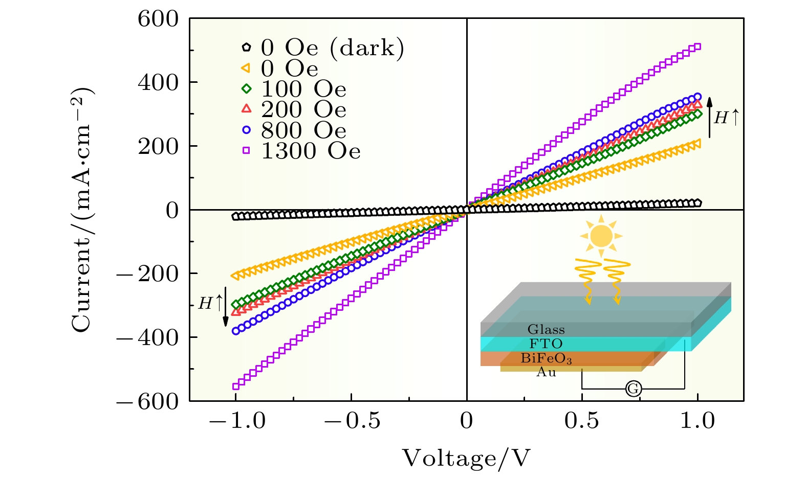
图 3 室温下样品J-V曲线在无磁场黑暗条件下及光照下随外磁场增强的响应情况
Fig. 3. The J-V curves of the sample at room temperature under dark conditions without magnetic field and under light with the increase of external magnetic field.
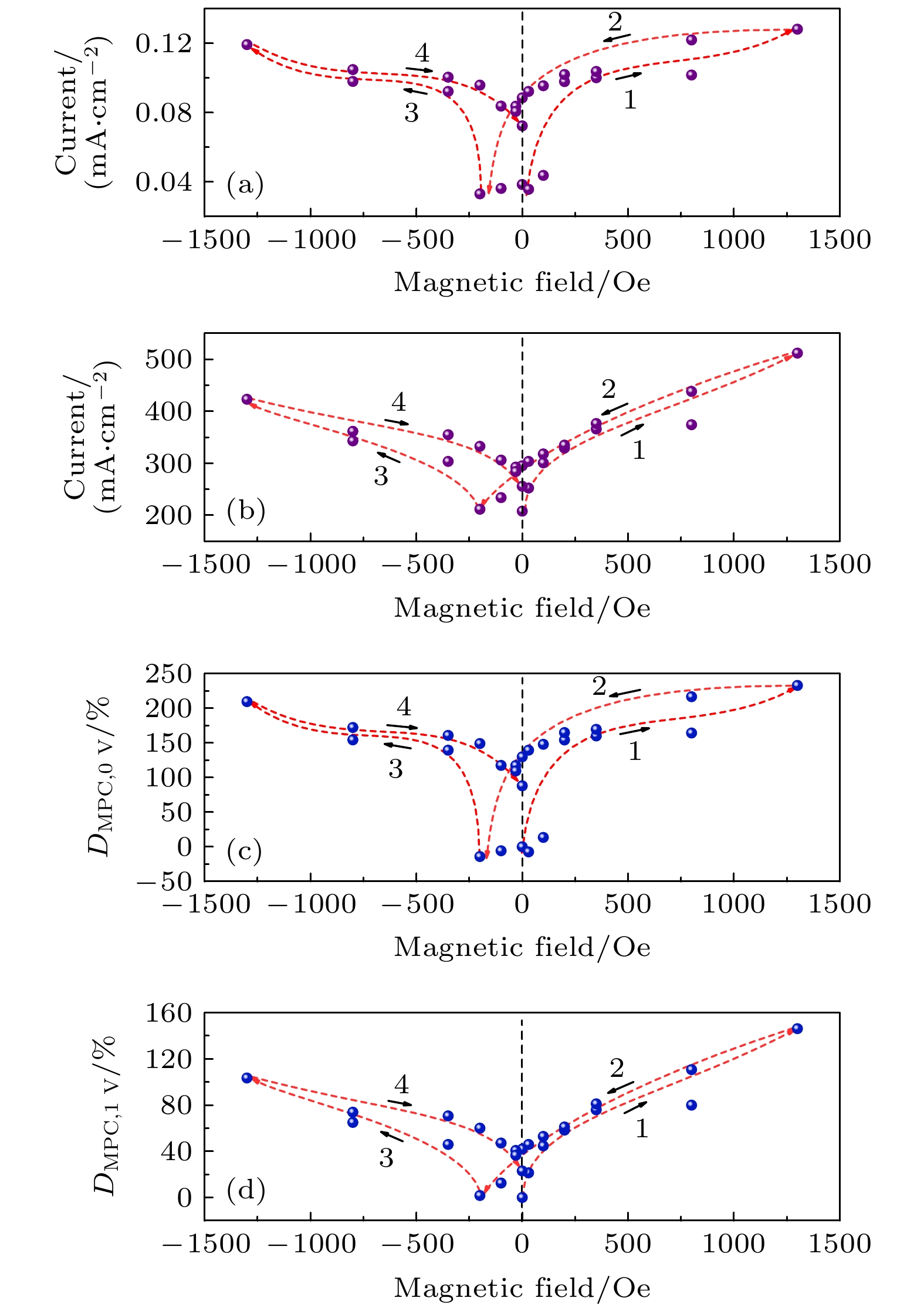
图 4 在偏压分别为(a), (c) 0 V和(b), (d) 1 V时, 室温下样品的(a), (b)光电流随磁场变化曲线以及(c), (d)
$ {D}_{{\rm{M}}{\rm{P}}{\rm{C}},{\rm{V}}} $ 值随磁场变化的响应曲线Fig. 4. Change curves of photocurrent (a), (b) and
$ {D}_{{\rm{M}}{\rm{P}}{\rm{C}},{\rm{V}}} $ (c), (d) with the alteration of magnetic field for the sample at room temperature with the bias of (a), (c) 0 V and (b), (d) 1 V. -
[1] Guo R, You L, Zhou Y, Shiuh L Z, Zou X, Chen L, Ramesh R, Wang J L 2013 Nat. Commun. 4 1990
Google Scholar
[2] Wei M C, Liu M F, Yang L, Xie B, Li X, Wang X Z, Cheng X Y, Zhu Y D, Li Z J, Su Y L, Li M Y, Hu Z Q, Liu J M 2020 Ceram. Int. 46 5126
Google Scholar
[3] Thakoor S 1992 Appl. Phys. Lett. 60 3319
Google Scholar
[4] 张亚菊, 谢忠帅, 郑海务, 袁国亮 2020 物理学报 69 127709
Google Scholar
Zhang Y J, Xie Z S, Zheng H W, Yuan G L 2020 Acta Phys. Sin. 69 127709
Google Scholar
[5] Wang J, Ma J, Yang Y B, Chen M F, Zhang J X, Ma J, Nan C W 2019 ACS Appl. Electron. Mater. 1 862
Google Scholar
[6] Li J K, Ge C, Jin K J, Du J Y, Yang J T, Lu H B, Yang G Z 2017 Appl. Phys. Lett. 110 142901
Google Scholar
[7] Wang X D, Wang P, Wang J L, Hu W D, Zhou X H, Guo N, Huang H, Sun S, Shen H, Lin T, Tang M H, Liao L, Jiang A Q, Sun J L, Meng X J, Chen X S, Lu W, Chu J H 2015 Adv. Mater. 27 6575
Google Scholar
[8] Wang P, Wang Y, Ye L, Wu M Z, Xie R Z, Wang X D, Chen X S, Fan Z Y, Wang J L, Hu W D 2018 Small 14 e1800492
Google Scholar
[9] Zhao Q L, He G P, Di J J, Song W L, Hou Z L, Tan P P, Wang D W, Cao M S 2017 ACS Appl. Mater. Interfaces 9 24696
Google Scholar
[10] Sujoy K G, Jinyoung K, Minsoo P K, Sangyun N, Jeonghoon C, Jae J K, Hyunhyub K 2022 ACS Nano 16 11415
Google Scholar
[11] Huangfu G, Xiao H, Guan L, Zhong H, Hu C, Shi Z, Guo Y 2020 ACS Appl. Mater. Interfaces 12 33950
Google Scholar
[12] Tan Z W, Hong L Q, Fan Z, Tian J J, Zhang L Y, Jiang Y, Hou Z P, Chen D Y, Qin M H, Zeng M, Gao J W, Lu X B, Zhou G F, Gao X S, Liu J M 2019 NPG Asia Mater. 11 20
Google Scholar
[13] Nechache R, Harnagea C, Li S, Cardenas L, Huang W, Chakrabartty J, Rosei F 2015 Nat. Photonics 9 61
Google Scholar
[14] Grinberg I, West D V, Torres M, Gou G Y, Stein D M, Wu L Y, Chen G N, Gallo E M, Akbashev A R, Davies P K, Spanier J E, Rappe A M 2013 Nature 503 509
Google Scholar
[15] Chakrabartty J, Harnagea C, Celikin M, Rosei F, Nechache R 2018 Nat. Photonics 12 271
Google Scholar
[16] Liu C C, Sun H Y, Ma C, Chen Z W, Luo Z, Su T S, Yin Y W, Li X G 2020 IEEE Electron Device Lett. 41 42
Google Scholar
[17] Liu Y, Yao Y, Dong S, Yang S, Li X 2012 Phys. Rev. B 86 075113
Google Scholar
[18] Fan Z, Yao K, Wang J 2014 Appl. Phys. Lett. 105 162903
Google Scholar
[19] Basu S R, Martin L W, Chu Y H, Gajek M, Ramesh R, Rai R C, Xu X, Musfeldt J L 2008 Appl. Phys. Lett. 92 091905
Google Scholar
[20] Ema K, Umeda K, Toda M, Yajima C, Arai Y, Kunugita H, Wolverson D, Davies J J 2006 Phys. Rev. B 73 241310
Google Scholar
[21] Hsiao Y C, Wu T, Li M, Hu B 2015 Adv. Mater. 27 2899
Google Scholar
[22] Pavliuk M V, Fernandes D L A, El-Zohry A M, Abdellah M, Nedelcu G, Kovalenko M V, Sa J 2016 Adv. Opt. Mater. 4 2004
Google Scholar
[23] Zhang C, Sun D, Sheng C X, Zhai Y X, Mielczarek K, Zakhidov A, Vardeny Z V 2015 Nat. Phys. 11 427
Google Scholar
[24] Even J, Pedesseau L, Jancu J M, Katan C 2014 Phys. Status Solidi-Rapid Res. Lett. 8 31
Google Scholar
[25] Pan R, Wang K, Li Y, Yu H, Li J, Xu L 2021 Adv. Electron. Mater. 7 2100026
Google Scholar
[26] Andy E 2019 Nature 570 429
Google Scholar
[27] Tomas L, Kevin A B, Rohit P, Michael D M 2018 Nat. Energy 3 828
Google Scholar
[28] Kevin A B, Axel F P, Zhengshan J Y, Mathieu B, Rongrong C, Jonathan P M, David P M, Robert L Z H, Colin D B, Tomas L, Ian M P, Maxmillian C M, Nicholas R, Rohit P, Sarah S, Duncan H, Wen M, Farhad M, Henry J S, Tonio B, Zachary C H, Stacey F B, Michael D M 2017 Nat. Energy 2 17009
Google Scholar
[29] Florent S, Jérémie W, Brett A K, Matthias B, Raphaël M, Bertrand P S, Loris B, Laura D, Juan J D L, Davide S, Gianluca C, Matthieu D, Mathieu B, Sylvain N, Quentin J, Bjoern N, Christophe B 2018 Nat. Mater. 17 820
Google Scholar
[30] Chen B, Yu Z S, Liu K, et al. 2019 Joule 3 177
Google Scholar
[31] Martin A G, Stephen P B 2017 Nat. Mater. 16 23
Google Scholar
[32] Pabitra K N, Suhas M, Henry J S, David C 2019 Nat. Rev. Mater. 4 269
Google Scholar
[33] Yuan Y B, Xiao Z G, Yang B, Huang J S 2014 J. Mater. Chem. A 2 6027
Google Scholar
[34] 蔡田怡, 雎胜 2018 物理学报 67 157801
Google Scholar
Cai T Y, Ju S 2018 Acta Phys. Sin. 67 157801
Google Scholar
[35] Yang S Y, Seidel J, Byrnes S J, Shafer P, Yang C H, Rossell M D, Yu P, Chu Y H, Scott J F, Ager III J W, Martin L W, Ramesh R 2010 Nat. Nanotechnol. 5 143
Google Scholar
[36] Guo R, You L, Lin W N, et al. 2020 Nat. Commun. 11 2571
Google Scholar
[37] Jhonata R V, Gislayne R A S, Márcio R M 2022 Int J Appl Ceram Technol. 19 1779
Google Scholar
[38] Ma G, Jiang W, Sun W, Yan Z, Sun B, Li S, Zhang M, Wang X, Gao A, Dai J, Liu Z, Li P, Tang W 2021 Phys. Scr. 96 125823
Google Scholar
[39] Pal S, Sarath N V, Priya K S, Murugavel P 2022 J. Phys. D Appl. Phys. 55 283001
Google Scholar
[40] Seung M L, Ahra C, Yong S C 2016 RSC Adv. 6 16602
Google Scholar
[41] Jin C, Li X W, Han W Q, et al. 2021 ACS Appl. Mater. Interfaces 13 41315
Google Scholar
[42] Guo D, Liu H, Li P, Wu Z, Wang S, Cui C, Li C, Tang W 2017 ACS Appl. Mater. Interfaces 9 1619
Google Scholar
[43] Xu H, Lin Y, Harumoto T, Shi J, Nan C 2017 ACS Appl. Mater. Interfaces 9 30127
Google Scholar
[44] Lu W, Fan Z, Yang Y, Ma J, Lai J, Song X, Zhuo X, Xu Z, Liu J, Hu X, Zhuo S, Xiu F, Cheng J, Sun D 2022 Nat. Commun. 13 1623
Google Scholar
[45] Yao Q, Liu W, Zhang R, Ma Y, Wang Y, Hu R, Mao W, Pu Y, Li X 2019 ACS Sustainable Chem. Eng. 7 12439
Google Scholar
[46] Sun D, Ehrenfreund E, Vardeny Z V 2014 Chem. Commun. 50 1781
Google Scholar
[47] Sagar R U R, Zhang X, Wang J, Xiong C 2014 J. Appl. Phys. 115 123708
Google Scholar
[48] Gautam B R, Nguyen T D, Ehrenfreund E, Vardeny Z V 2012 Phys. Rev. B 85 205207
Google Scholar
[49] Wang J, Chepelianskii A, Gao F, Greenham N C 2012 Nat. Commun. 3 1191
Google Scholar
[50] Hu B, Yan L, Shao M 2009 Adv. Mater. 21 1500
Google Scholar
[51] Devir-Wolfman A H, Khachatryan B, Gautam B R, Tzabary L, Keren A, Tessler N, Vardeny Z V, Ehrenfreund E 2014 Nat. Commun. 5 4529
Google Scholar
[52] Muneeswaran M, Giridharan N V 2014 J. Appl. Phys. 115 214109
Google Scholar
[53] Sharma G N, Dutta S, Singh S K, Chatterjee R 2016 Mater. Res. Express 3 106202
Google Scholar
[54] Wang J J, Hu J M, Yang T N, Feng M, Zhang J X, Chen L Q, Nan C W 2014 Sci. Rep. 4 4553
Google Scholar
[55] Wei S, Wenxuan W, Dong C, Zhenxiang C, Tingting J, Yuanxu W 2019 J. Phys. Chem. C 123 16393
Google Scholar
[56] Tan K H, Chen Y W, Van Nguyen C, et al. 2019 ACS Appl. Mater. Interfaces 11 1655
Google Scholar
[57] Lu Y, Fan Z, Liang F, Yang Z, Liang Z T, Zeyu Z, Guohong M, Daniel S, Andrivo R, Le W, Lei C, Andrew M R, Junling W 2018 Sci. Adv. 4 eaat3438
Google Scholar
[58] 翟宏如, 都有为, 韩秀峰, 刘俊明, 王克锋, 赵建华, 邓加军, 郑厚植, 邢定钰, 夏钶, 周仕明, 苏刚, 蔡建旺 2013 自旋电子学 (北京: 科学出版社) 第459, 460页
Zhai H R, Du Y Y, Han X F, Liu J M, Wang K F, Zhao J H, Deng J J, Zheng H Z, Xing D Y, Xia K, Zhou S M, Su G, Cai J W 2013 Spintronics (Beijing: Science Press) pp459, 460 (in Chinese)

 下载:
下载:


计量
- 文章访问数: 9942
- PDF下载量: 191
- 被引次数: 0
