


-
In recent years, due to their unique physical, chemical and electronic properties, two-dimensional materials have received more and more researchers’ attention. In particular, the excellent optoelectronic properties and transport properties of two-dimensional materials such as graphene, black phosphorous and transition metal sulfide materials make them have broad application prospects in the field of next-generation optoelectronic devices. In this article, we will mainly introduce the advantages of two-dimensional materials in the field of photodetection, outline the basic principles and parameters of photodetectors, focus on the difference between the grating effect and the traditional photoconductive effect, and the reasons and characteristics of improving optical gain and optical responsivity. Then we review the latest developments and applications of grating local control in photodetectors, and finally summarize the problems faced by the photodetectors of this kind and their prospects for the future.
-
Keywords:
- two-dimensional material /
- photoelectric detection /
- photogating effect /
- heterojunction /
- built-in electric field
[1] Novoselov K S, Mishchenko A, Carvalho A, Castro Neto A H 2016 Science 355 aac9439
[2] Novoselov K S, Geim A K, Morozov S V, Jiang D, Katsnelson M I, Grigorieva I V, Dubonos S V, Firsov A A 2005 Nature 438 197
 Google Scholar
[3] Novoselov K S, Jiang Z, Zhang Y, Morozov S V, Stormer H L, Zeitler U, Maan J C, Boebinger G S, Kim P, Geim A K 2007 Science 315 1379
Google Scholar
[4] Butler S Z, Hollen S M, Cao L, Cui Y, Gupta J A, Gutierrez H R, Heinz T F, Hong S S, Huang J, Ismach A F, Johnston Halperin E, Kuno M, Plashnitsa V V, Robinson R D, Ruoff R S, Salahuddin S, Shan J, Shi L, Spencer M G, Terrones M, Windl W, Goldberger J E 2013 ACS Nano 7 2898
Google Scholar
[5] Geim A K 2009 Science 324 1530
Google Scholar
[6] Liu C H, Chang Y C, Norris T B, Zhong Z 2014 Nat. Nanotechnol. 9 273
Google Scholar
[7] Koppens F H, Mueller T, Avouris P, Ferrari A C, Vitiello M S, Polini M 2014 Nat. Nanotechnol. 9 780
Google Scholar
[8] Wang Q H, Kalantar Zadeh K, Kis A, Coleman J N, Strano M S 2012 Nat. Nanotechnol. 7 699
Google Scholar
[9] Choi W, Choudhary N, Han G H, Park J, Akinwande D, Lee Y H 2017 Mater. Today 20 116
Google Scholar
[10] Chen P, Li N, Chen X, Ong W J, Zhao X 2017 2D Materials 5 014002
[11] Guo Z, Chen S, Wang Z, Yang Z, Liu F, Xu Y, Wang J, Yi Y, Zhang H, Liao L, Chu P K, Yu X F 2017 Adv. Mater. 29 1703811
Google Scholar
[12] Brar V W, Jang M S, Sherrott M, Kim S, Lopez J J, Kim L B, Choi M, Atwater H 2014 Nano Lett. 14 3876
Google Scholar
[13] Liu L, Feng Y P, Shen Z X 2003 Phys. Rev. B 68 104102
Google Scholar
[14] Wang J, Fang H, Wang X, Chen X, Lu W, Hu W 2017 Small 13 1700894
Google Scholar
[15] Zhang H 2015 ACS Nano 9 9451
Google Scholar
[16] Ren Y X, Dai T J, He B, Liu X Z 2019 Ieee Electron Device Lett. 40 48
Google Scholar
[17] Guo Q S, Pospischil A, Bhuiyan M, Jiang H, Tian H, Farmer D, Deng B C, Li C, Han S J, Wang H, Xia Q F, Ma T P, Mueller T, Xia F N 2016 Nano Lett. 16 4648
Google Scholar
[18] Li L, Wang W K, Chai Y, Li H Q, Tian M L, Zhai T Y 2017 Adv. Funct. Mater. 27 1701011
Google Scholar
[19] Li J, Niu L, Zheng Z, Yan F 2014 Adv. Mater. 26 5239
Google Scholar
[20] Park H S, Ha T J, Hong Y, Lee J H, Lee B J, You B H, Kim N D, Han M K 2008 JSID 16 1165
Google Scholar
[21] Aiello A, Hoque A K M H, Baten M Z, Bhattacharya P 2019 ACS Photonics 6 1289
Google Scholar
[22] Son D I, Kim T W, Shim J H, Jung J H, Lee D U, Lee J M, Park W I, Choi W K 2010 Nano Lett. 10 2441
Google Scholar
[23] Gwon H, Kim H S, Lee K U, Seo D H, Park Y C, Lee Y S, Ahn B T, Kang K 2011 Energy Environ. Sci. 4 1277
Google Scholar
[24] Long M, Wang P, Fang H, Hu W 2018 Adv. Funct. Mater. 29 1803807
[25] Colace L, Masini G, Galluzzi F, Assanto G, Capellini G, Di Gaspare L, Palange E, Evangelisti F 1998 Appl. Phys. Lett. 72 3175
Google Scholar
[26] Petritz R L 1956 APS 104 1508
[27] Jie J S, Zhang W J, Jiang Y, Meng X M, Li Y Q, Lee S T 2006 Nano Lett. 6 1887
Google Scholar
[28] Huang H, Wang J, Hu W, Liao L, Wang P, Wang X, Gong F, Chen Y, Wu G, Luo W, Shen H, Lin T, Sun J, Meng X, Chen X, Chu J 2016 Nanotechnology 27 445201
Google Scholar
[29] Rubinelli F A 2016 Thin Solid Films 619 102
Google Scholar
[30] Kondo T, Hayafuji J J, Munekata H 2006 Jpn. J. Appl. Phys. 45 L663
Google Scholar
[31] Ellsworth D, Lu L, Lan J, Chang H, Li P, Wang Z, Hu J, Johnson B, Bian Y, Xiao J, Wu R, Wu M 2016 Nature Phys. 12 861
Google Scholar
[32] Xu X, Gabor N M, Alden J S, Van Der Zande A M, McEuen P L 2010 Nano Lett. 10 562
Google Scholar
[33] Buscema M, Barkelid M, Zwiller V, Van Der Zant H S J, Steele G A, Castellanos Gomez A 2013 Nano Lett. 13 358
Google Scholar
[34] Huang M, Wang M, Chen C, Ma Z, Li X, Han J, Wu Y 2016 Adv. Mater. 28 3481
Google Scholar
[35] Island J O, Blanter S I, Buscema M, van der Zant H S J, Castellanos Gomez A 2015 Nano Lett. 15 7853
Google Scholar
[36] Murali K, Abraham N, Das S, Kallatt S, Majumdar K 2019 ACS Appl. Mater. Interfaces 11 30010
Google Scholar
[37] Zhou X, Hu X, Zhou S, Song H, Zhang Q, Pi L, Li L, Li H, Lu J, Zhai T 2018 Adv. Mater. 30 1703286
Google Scholar
[38] Kim J, Park V, Jang H, et al. 2017 ACS Photonics 4 482
Google Scholar
[39] Wang F, Zhang Y, Gao Y, Luo P, Su J, Han W, Liu K, Li H, Zhai T 2019 Small 15 e1901347
Google Scholar
[40] Furchi M M, Polyushkin D K, Pospischil A, Mueller T 2014 Nano Lett. 14 6165
Google Scholar
[41] Zhu J L, Zhang G, Wei J, Sun J L 2012 Appl. Phys. Lett. 101 123117
Google Scholar
[42] Lui C H, Frenzel A J, Pilon D V, Lee Y H, Ling X, Akselrod G M, Kong J, Gedik N 2014 Phys. Rev. Lett. 113 166801
Google Scholar
[43] Nakanishi H, Bishop K J, Kowalczyk B, Nitzan A, Weiss E A, Tretiakov K V, Apodaca M M, Klajn R, Stoddart J F, Grzybowski B A 2009 Nature 460 371
Google Scholar
[44] Fang H H, Hu W D 2017 Adv. Sci. 4 1700323
Google Scholar
[45] Wang L, Zou X, Lin J, Jiang J, Liu Y, Liu X, Zhao X, Liu Y F, Ho J C, Liao L 2019 ACS Nano 13 4804
Google Scholar
[46] Deng Y, Luo Z, Conrad N J, Liu H, Gong Y, Najmaei S, Ajayan P M, Lou J, Xu X, Ye P D 2014 ACS Nano 8 8292
Google Scholar
[47] Zhu W, Yogeesh M N, Yang S, Aldave S H, Kim J S, Sonde S, Tao L, Lu N, Akinwande D 2015 Nano Lett. 15 1883
Google Scholar
[48] Schütz M, Maschio L, Karttunen A J, Usvyat D 2017 J. Phys. Chem. Lett. 8 1290
Google Scholar
[49] Sun L, Lin Z, Peng J, Weng J, Huang Y, Luo Z 2015 Sci. Rep. 4 4794
Google Scholar
[50] Hanlon D, Backes C, Doherty E, et al. 2015 Nat. Commun. 6 8563
Google Scholar
[51] Smith J B, Hagaman D, Ji H F 2016 Nanotechnology 27 215602
Google Scholar
[52] Reina A, Jia X, Ho J, Nezich D, Son H, Bulovic V, Dresselhaus M S, Kong J 2009 Nano Lett. 9 30
Google Scholar
[53] Liu C H, Dissanayake N M, Lee S, Lee K, Zhong Z 2012 ACS Nano 6 7172
Google Scholar
[54] Gabor N M, Song J C W, Ma Q, Nair N L, Taychatanapat T, Watanabe K, Taniguchi T, Levitov L S, Jarillo Herrero P 2011 Science 334 648
Google Scholar
[55] Guo X, Wang W, Nan H, Yu Y, Jiang J, Zhao W, Li J, Zafar Z, Xiang N, Ni Z, Hu W, You Y, Ni Z 2016 Optica 3 1066
Google Scholar
[56] Howell S W, Ruiz I, Davids P S, Harrison R K, Smith S W, Goldflam M D, Martin J B, Martinez N J, Beechem T E 2017 Sci. Rep. 7 14651
Google Scholar
[57] Yu X, Dong Z, Liu Y, Liu T, Tao J, Zeng Y, Yang J K W, Wang Q J 2016 Nanoscale 8 327
Google Scholar
[58] Zhang K, Peng M, Yu A, Fan Y, Zhai J, Wang Z L 2019 Mater. Horizons 6 826
Google Scholar
[59] Fukushima S, Shimatani M, Okuda S, Ogawa S 2018 Appl. Phys. Lett. 113 061102
Google Scholar
[60] Cao G, Wang F, Peng M, Shao X, Yang B, Hu W, Li X, Chen J, Shan Y, Wu P, Hu L, Liu R, Gong H, Cong C, Qiu Z J 2020 Adv. Electron. Mater. 6 1901007
Google Scholar
[61] Zhang W, Huang J K, Chen C H, Chang Y H, Cheng Y J, Li L J 2013 Adv. Mater. 25 3456
Google Scholar
[62] Miller B, Parzinger E, Vernickel A, Holleitner A W, Wurstbauer U 2015 Appl. Phys. Lett. 106 122103
Google Scholar
[63] Kufer D, Konstantatos G 2015 Nano Lett. 15 7307
Google Scholar
[64] Han P, Adler E R, Liu Y J, St Marie L, El Fatimy A, Melis S, Van Keuren E, Barbara P 2019 Nanotechnology 30 284004
Google Scholar
[65] Deng J N, Zong L Y, Zhu M S, Liao F Y, Xie Y Y, Guo Z X, Liu J, Lu B R, Wang J L, Hu W D, Zhou P, Bao W Z, Wan J 2019 Adv. Funct. Mater. 19 06242
[66] Tu L, Cao R, Wang X, Chen Y, Wu S, Wang F, Wang Z, Shen H, Lin T, Zhou P, Meng X, Hu W, Liu Q, Wang J, Liu M, Chu J 2020 Nat. Commun. 11 101
Google Scholar
[67] Thakar K, Mukherjee B, Grover S, Kaushik N, Deshmukh M, Lodha S 2018 ACS Appl. Mater. Interfaces 10 36512
Google Scholar
[68] Velický M, Bradley D F, Cooper A J, Hill E W, Kinloch I A, Mishchenko A, Novoselov K S, Patten H V, Toth P S, Valota A T, Worrall S D, Dryfe R A W 2014 ACS Nano 8 10089
Google Scholar
[69] Zhang B Y, Liu T, Meng B, Li X, Liang G, Hu X, Wang Q J 2013 Nat. Commun. 4 1811
Google Scholar
[70] Freitag M, Low T, Zhu W, Yan H, Xia F, Avouris P 2013 Nat. Commun. 4 1951
Google Scholar
[71] Echtermeyer T J, Britnell L, Jasnos P K, Lombardo A, Gorbachev R V, Grigorenko A N, Geim A K, Ferrari A C, Novoselov K S 2011 Nat. Commun. 2 458
Google Scholar
[72] Low T, Avouris P 2014 ACS Nano 8 1086
Google Scholar
[73] Novoselov K S, Jiang D, Schedin F, Booth T J, Khotkevich V V, Morozov S V, Geim A K 2005 PNAS 102 10451
Google Scholar
[74] Xia F, Mueller T, Golizadeh Mojarad R, Freitag M, Lin Y M, Tsang J, Perebeinos V, Avouris P 2009 Nano Lett. 9 1039
Google Scholar
[75] Liu Y, Cheng R, Liao L, Zhou H, Bai J, Liu G, Liu L, Huang Y, Duan X 2011 Nat. Commun. 2 579
Google Scholar
[76] Furchi M, Urich A, Pospischil A, Lilley G, Unterrainer K, Detz H, Klang P, Andrews A M, Schrenk W, Strasser G, Mueller T 2012 Nano Lett. 12 2773
Google Scholar
[77] Roy K, Padmanabhan M, Goswami S, Sai T P, Ramalingam G, Raghavan S, Ghosh A 2013 Nature Nanotech. 8 826
Google Scholar
[78] Qiao H, Yuan J, Xu Z, Chen C, Lin S, Wang Y, Song J, Liu Y, Khan Q, Hoh H Y, Pan C X, Li S, Bao Q 2015 ACS Nano 9 1886
Google Scholar
[79] Wang N, West D, Duan W, Zhang S B 2019 Nanoscale Adv. 1 470
Google Scholar
[80] Liu Y, Weinert M, Li L 2012 APS 108 115501
[81] Xu J, Song Y J, Park J H, Lee S 2018 Solid State Electron. 144 86
Google Scholar
[82] Liu Y, Shivananju B N, Wang Y, Zhang Y, Yu W, Xiao S, Sun T, Ma W, Mu H, Lin S, Zhang H, Lu Y, Qiu C W, Li S, Bao Q 2017 ACS Appl. Mater. Interfaces 9 36137
Google Scholar
[83] Liu B Y, You C Y, Zhao C, Shen G L, Liu Y W, Li Y F, Yan H, Zhang Y Z 2019 Chin. Opt. Lett. 17 020002
Google Scholar
[84] Lan C, Li C, Wang S, He T, Zhou Z, Wei D, Guo H, Yang H, Liu Y 2017 J. Mater. Chem. C 5 1494
Google Scholar
[85] Kang B, Kim Y, Yoo W J, Lee C 2018 Small 14 1802593
Google Scholar
[86] Yu W, Li S, Zhang Y, Ma W, Sun T, Yuan J, Fu K, Bao Q 2017 Small 13 1700268
Google Scholar
[87] Zhang W, Chuu C P, Huang J K, Chen C H, Tsai M L, Chang Y H, Liang C T, Chen Y Z, Chueh Y L, He J H, Chou M Y, Li L J 2014 Sci. Rep. 4 3826
[88] Chang P H, Li C S, Fu F Y, Huang K Y, Chou A S, Wu C I 2018 Adv. Funct. Mater. 28 1800179
Google Scholar
[89] Qi Z Y, Yang T F, Li D, Li H L, Wang X, Zhang X H, Li F, Zheng W H, Fan P, Zhuang X J, Pan A L 2019 Mater. Horizons 6 1474
Google Scholar
[90] Yang T, Zheng B, Wang Z, Xu T, Pan C, Zou J, Zhang X, Qi Z, Liu H, Feng Y, Hu W, Miao F, Sun L, Duan X, Pan A 2017 Nat. Commun. 8 1906
Google Scholar
[91] Krause M, Dent E W, Bear J E, Loureiro J J, Gertler F B 2003 Annu. Rev. Cell. Dev. Biol. 19 541
Google Scholar
[92] Shim J, Kang D H, Kim Y, Kum H, Kong W, Bae S H, Almansouri I, Lee K, Park J H, Kim J 2018 Carbon 133 78
Google Scholar
[93] Ye L, Wang P, Luo W J, Gong F, Liao L, Liu T D, Tong L, Zang J F, Xu J B, Hu W D 2017 Nano Energy 37 53
Google Scholar
[94] Guo N, Xiao L, Gong F, Luo M, Wang F, Jia Y, Chang H, Liu J, Li Q, Wu Y, Wang Y, Shan C, Xu Y, Zhou P, Hu W 2020 Adv. Science 7 1901637
Google Scholar
-

图 1 光栅效应特性 (a) 光栅效应示意图[39]; (b) 光照后, 转移特性曲线
${I}_{\mathrm{d}\mathrm{s}}\text-{V}_{\mathrm{g}}$ , 其中, 黑线、红线和蓝线分别代表暗电流、光栅效应下的光电流以及光栅效应和光电导效应的叠加的光电流; (c)光栅效应器件中的能带排布示意图[44].Fig. 1. The characteristics of the photogating effect: (a) Schematic diagram of the photogating effect[39]; (b) the
${I}_{\mathrm{d}\mathrm{s}}\text-{V}_{\mathrm{g}}$ transfer chara-cteristic curve after illumination. The black line, red line and blue line represent dark current, photocurrent of photogating effect, the superimposed photocurrent of photogating effect and photoconductive effect, respectively; (c) schematic diagram of band arrangement in photogating effect devices[44].
图 2 单一二维材料光电探测器 (a) 双层石墨烯异质结中的光激发热载流子隧穿[6]; (b) p型轻掺杂Si/SiO2衬底上的石墨烯光电探测器的示意图[55]; (c) p型InSb衬底上石墨烯场效应晶体管的示意图[59]; (d) 电荷陷阱模型和简化的能带图[40]; (e) 光响应度与顶栅Vtg的关系[65]; (f) 不同衬底下的光响应度[58]; (g) 在不同入射功率下, 在最大跨导附近实现最大光电流[35]; (h) 光电流与时间的关系[67].
Fig. 2. Single two-dimensional material photodetector: (a) Photoexcited hot carrier tunnelling in graphene double-layer heterostructures[6]; (b) schematic diagram of the graphene photodetector on lightly p-doped silicon/SiO2 substrate[55]; (c) schematic diagram of the InSb-based graphene field effect transistor (FET)[59]; (d) charge trapping model and simplified energy band diagram[40]; (e) the relationship between photoresponsivity and Vtg[65]; (f) photoresponsivity under different substrates[58]; (g) the maximum photocurrent is realized near the maximum transconductance at different incident power[35]; (h) the relationship between photocurrent and time[67].
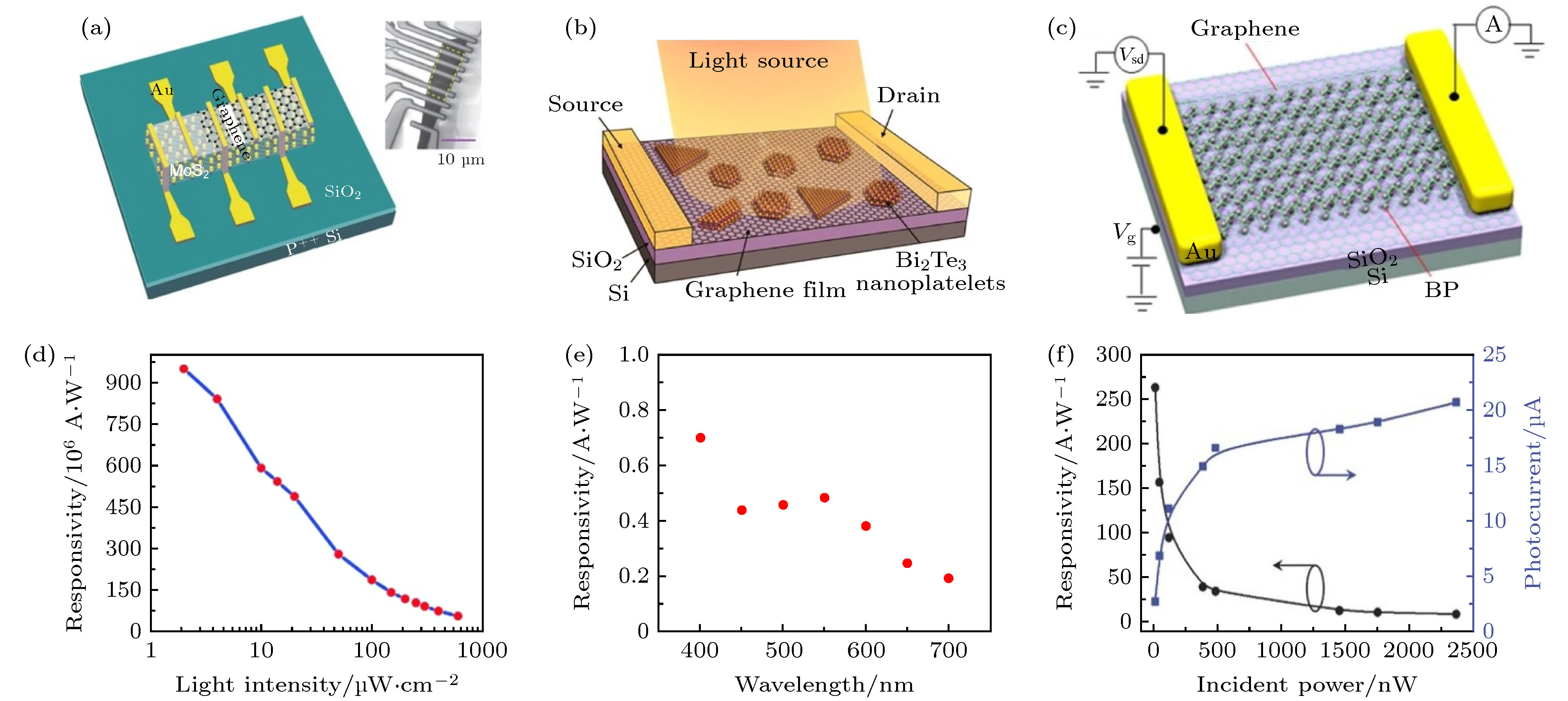
图 3 石墨烯异质结光电探测器: (a) 石墨烯/ MoS2异质结光电探测器的示意图; (b) 石墨烯/Bi2Te3异质结光电探测器的示意图; (c) 石墨烯/BP异质结光电探测器的示意图; (d)光响应度与光照强度的关系; (e)光响应度与波长的关系(VD = –3 V, VG = –30 V); (f)在波长为980 nm, 光电流和光响应随入射光强的关系 (VDS = 1 V, VG = 0 V).
Fig. 3. The photodetectors based on graphene heterostructures: (a) Schematic of device architecture graphene/MoS2 photodetector[77]; (b) schematic of the heterostructure phototransistor device[78]; (c) graphene/BP heterostructure photodetector[82]; (d) the relationship between photoresponsivity and light intensity[89]; (e) responsivity as a function of the wavelength (VD = –3 V, VG = –30 V)[85]; (f) photocurrent and photoresponsivity versus incident light power at 980 nm. (VDS = 1 V, VG = 0 V)[86].

图 4 基于光栅效应的PN异质结光电探测器 (a) PbI2/WS2异质结构光电探测器; (b) PbI2/WS2光电探测器的光响应时间[89]; (c) WSe2 /SnS2多电极异质结构背栅器件的示意图; (d) WSe2/SnS2异质结的能带结构和光激发、层间弛豫过程的示意图[90]; (e)基于光栅效应的WSe2/BP光电探测器示意图; (f) 在1 mW/cm2的入射功率密度和0.5 V偏置下, 光增益G和探测率D对不同波长照明的依赖关系[93]; (g) 在637 nm光照下器件的示意图; (h)顶栅电极侧面和重叠区域之间形成导电通道Vtg; (i)一个调制周期: 上升时间为10 µs、下降时间为10 µs的快速分量和20 µs的慢速分量组成[94].
Fig. 4. PN heterojunction photodetector based on photogating effect: (a) Schematic device structure of PbI2/WS2 photodetector fabricated on SiO2/Si substrate; (b) time-resolved photoresponse of PbI2/WS2 phototransistors[89]; (c) schematic diagram of the multi-electrode WSe2/SnS2 vdW heterostructure backgate device; (d) schematic diagram of WSe2/SnS2 heterostructure band structure and photoexcitation, interlayer relaxation process in WSe2/SnS2 heterojunction[90]; (e) schematic illustration of the BP on WSe2 photodetector with photogate structure; (f) the dependence of the photogain
$ G $ and detectivity$ {D}^{*} $ on the different wavelength illumination at 1 mW/cm2 incident illumination power density and 0.5 V bias[93]; (g) schematic illustration of the device in the dark under 637 nm illumination; (h) a conductive path for Vtg is formed between side top-gate electrode and overlapped region; (i) a single modulation cycle The rise time is ≈10 µs The fall time consists of a fast component of ≈10 µs and a slow component of ≈ 20 µs[94].
图 5 基于光栅效应的光电探测器新结构 (a)器件结构示意图; (b)器件结构能带图
Fig. 5. New structure of photodetector based on photogating effect: (a) Schematic diagram of device structure; (b) sche-matic diagram of energy band structure
表 1 基于石墨烯异质结(Gr)的光栅局域调控光电探测器
Table 1. Graphene(Gr)-based photodetectors with grating photogating.
Material Responsivity/(A·W–1) Gain Response time/ms Detection range/nm Ref. Gr/MoSe2 1.3 × 10⁴ — 22000.0 550 [83] Gr/MoTe2 970.82 4.69 × 10⁸ 78.0 1064 [86] Gr/ReS2 7 × 10⁵ — 30.0 550 nm [85] Gr/WS2 950 — — 340–680 nm [84] Gr/MoS2 107 108 — 650 [87] Gr/BP 55.75 — 36.0 655 [82] Gr/BiI3 6 × 10⁶ — 8.0 532 [88] Gr/PbSe 6613 7824 25.0 — [16] Gr/Bi2Te3 35 83 8.7 532—1550 [78] Gr/MoS2 5 × 10⁸ — — 635 [77] Gr/Bi2Se3 8.18 — — near-IR 750—2500 [38]  下载: 导出CSV
-
[1] Novoselov K S, Mishchenko A, Carvalho A, Castro Neto A H 2016 Science 355 aac9439
[2] Novoselov K S, Geim A K, Morozov S V, Jiang D, Katsnelson M I, Grigorieva I V, Dubonos S V, Firsov A A 2005 Nature 438 197
Google Scholar
[3] Novoselov K S, Jiang Z, Zhang Y, Morozov S V, Stormer H L, Zeitler U, Maan J C, Boebinger G S, Kim P, Geim A K 2007 Science 315 1379
Google Scholar
[4] Butler S Z, Hollen S M, Cao L, Cui Y, Gupta J A, Gutierrez H R, Heinz T F, Hong S S, Huang J, Ismach A F, Johnston Halperin E, Kuno M, Plashnitsa V V, Robinson R D, Ruoff R S, Salahuddin S, Shan J, Shi L, Spencer M G, Terrones M, Windl W, Goldberger J E 2013 ACS Nano 7 2898
Google Scholar
[5] Geim A K 2009 Science 324 1530
Google Scholar
[6] Liu C H, Chang Y C, Norris T B, Zhong Z 2014 Nat. Nanotechnol. 9 273
Google Scholar
[7] Koppens F H, Mueller T, Avouris P, Ferrari A C, Vitiello M S, Polini M 2014 Nat. Nanotechnol. 9 780
Google Scholar
[8] Wang Q H, Kalantar Zadeh K, Kis A, Coleman J N, Strano M S 2012 Nat. Nanotechnol. 7 699
Google Scholar
[9] Choi W, Choudhary N, Han G H, Park J, Akinwande D, Lee Y H 2017 Mater. Today 20 116
Google Scholar
[10] Chen P, Li N, Chen X, Ong W J, Zhao X 2017 2D Materials 5 014002
[11] Guo Z, Chen S, Wang Z, Yang Z, Liu F, Xu Y, Wang J, Yi Y, Zhang H, Liao L, Chu P K, Yu X F 2017 Adv. Mater. 29 1703811
Google Scholar
[12] Brar V W, Jang M S, Sherrott M, Kim S, Lopez J J, Kim L B, Choi M, Atwater H 2014 Nano Lett. 14 3876
Google Scholar
[13] Liu L, Feng Y P, Shen Z X 2003 Phys. Rev. B 68 104102
Google Scholar
[14] Wang J, Fang H, Wang X, Chen X, Lu W, Hu W 2017 Small 13 1700894
Google Scholar
[15] Zhang H 2015 ACS Nano 9 9451
Google Scholar
[16] Ren Y X, Dai T J, He B, Liu X Z 2019 Ieee Electron Device Lett. 40 48
Google Scholar
[17] Guo Q S, Pospischil A, Bhuiyan M, Jiang H, Tian H, Farmer D, Deng B C, Li C, Han S J, Wang H, Xia Q F, Ma T P, Mueller T, Xia F N 2016 Nano Lett. 16 4648
Google Scholar
[18] Li L, Wang W K, Chai Y, Li H Q, Tian M L, Zhai T Y 2017 Adv. Funct. Mater. 27 1701011
Google Scholar
[19] Li J, Niu L, Zheng Z, Yan F 2014 Adv. Mater. 26 5239
Google Scholar
[20] Park H S, Ha T J, Hong Y, Lee J H, Lee B J, You B H, Kim N D, Han M K 2008 JSID 16 1165
Google Scholar
[21] Aiello A, Hoque A K M H, Baten M Z, Bhattacharya P 2019 ACS Photonics 6 1289
Google Scholar
[22] Son D I, Kim T W, Shim J H, Jung J H, Lee D U, Lee J M, Park W I, Choi W K 2010 Nano Lett. 10 2441
Google Scholar
[23] Gwon H, Kim H S, Lee K U, Seo D H, Park Y C, Lee Y S, Ahn B T, Kang K 2011 Energy Environ. Sci. 4 1277
Google Scholar
[24] Long M, Wang P, Fang H, Hu W 2018 Adv. Funct. Mater. 29 1803807
[25] Colace L, Masini G, Galluzzi F, Assanto G, Capellini G, Di Gaspare L, Palange E, Evangelisti F 1998 Appl. Phys. Lett. 72 3175
Google Scholar
[26] Petritz R L 1956 APS 104 1508
[27] Jie J S, Zhang W J, Jiang Y, Meng X M, Li Y Q, Lee S T 2006 Nano Lett. 6 1887
Google Scholar
[28] Huang H, Wang J, Hu W, Liao L, Wang P, Wang X, Gong F, Chen Y, Wu G, Luo W, Shen H, Lin T, Sun J, Meng X, Chen X, Chu J 2016 Nanotechnology 27 445201
Google Scholar
[29] Rubinelli F A 2016 Thin Solid Films 619 102
Google Scholar
[30] Kondo T, Hayafuji J J, Munekata H 2006 Jpn. J. Appl. Phys. 45 L663
Google Scholar
[31] Ellsworth D, Lu L, Lan J, Chang H, Li P, Wang Z, Hu J, Johnson B, Bian Y, Xiao J, Wu R, Wu M 2016 Nature Phys. 12 861
Google Scholar
[32] Xu X, Gabor N M, Alden J S, Van Der Zande A M, McEuen P L 2010 Nano Lett. 10 562
Google Scholar
[33] Buscema M, Barkelid M, Zwiller V, Van Der Zant H S J, Steele G A, Castellanos Gomez A 2013 Nano Lett. 13 358
Google Scholar
[34] Huang M, Wang M, Chen C, Ma Z, Li X, Han J, Wu Y 2016 Adv. Mater. 28 3481
Google Scholar
[35] Island J O, Blanter S I, Buscema M, van der Zant H S J, Castellanos Gomez A 2015 Nano Lett. 15 7853
Google Scholar
[36] Murali K, Abraham N, Das S, Kallatt S, Majumdar K 2019 ACS Appl. Mater. Interfaces 11 30010
Google Scholar
[37] Zhou X, Hu X, Zhou S, Song H, Zhang Q, Pi L, Li L, Li H, Lu J, Zhai T 2018 Adv. Mater. 30 1703286
Google Scholar
[38] Kim J, Park V, Jang H, et al. 2017 ACS Photonics 4 482
Google Scholar
[39] Wang F, Zhang Y, Gao Y, Luo P, Su J, Han W, Liu K, Li H, Zhai T 2019 Small 15 e1901347
Google Scholar
[40] Furchi M M, Polyushkin D K, Pospischil A, Mueller T 2014 Nano Lett. 14 6165
Google Scholar
[41] Zhu J L, Zhang G, Wei J, Sun J L 2012 Appl. Phys. Lett. 101 123117
Google Scholar
[42] Lui C H, Frenzel A J, Pilon D V, Lee Y H, Ling X, Akselrod G M, Kong J, Gedik N 2014 Phys. Rev. Lett. 113 166801
Google Scholar
[43] Nakanishi H, Bishop K J, Kowalczyk B, Nitzan A, Weiss E A, Tretiakov K V, Apodaca M M, Klajn R, Stoddart J F, Grzybowski B A 2009 Nature 460 371
Google Scholar
[44] Fang H H, Hu W D 2017 Adv. Sci. 4 1700323
Google Scholar
[45] Wang L, Zou X, Lin J, Jiang J, Liu Y, Liu X, Zhao X, Liu Y F, Ho J C, Liao L 2019 ACS Nano 13 4804
Google Scholar
[46] Deng Y, Luo Z, Conrad N J, Liu H, Gong Y, Najmaei S, Ajayan P M, Lou J, Xu X, Ye P D 2014 ACS Nano 8 8292
Google Scholar
[47] Zhu W, Yogeesh M N, Yang S, Aldave S H, Kim J S, Sonde S, Tao L, Lu N, Akinwande D 2015 Nano Lett. 15 1883
Google Scholar
[48] Schütz M, Maschio L, Karttunen A J, Usvyat D 2017 J. Phys. Chem. Lett. 8 1290
Google Scholar
[49] Sun L, Lin Z, Peng J, Weng J, Huang Y, Luo Z 2015 Sci. Rep. 4 4794
Google Scholar
[50] Hanlon D, Backes C, Doherty E, et al. 2015 Nat. Commun. 6 8563
Google Scholar
[51] Smith J B, Hagaman D, Ji H F 2016 Nanotechnology 27 215602
Google Scholar
[52] Reina A, Jia X, Ho J, Nezich D, Son H, Bulovic V, Dresselhaus M S, Kong J 2009 Nano Lett. 9 30
Google Scholar
[53] Liu C H, Dissanayake N M, Lee S, Lee K, Zhong Z 2012 ACS Nano 6 7172
Google Scholar
[54] Gabor N M, Song J C W, Ma Q, Nair N L, Taychatanapat T, Watanabe K, Taniguchi T, Levitov L S, Jarillo Herrero P 2011 Science 334 648
Google Scholar
[55] Guo X, Wang W, Nan H, Yu Y, Jiang J, Zhao W, Li J, Zafar Z, Xiang N, Ni Z, Hu W, You Y, Ni Z 2016 Optica 3 1066
Google Scholar
[56] Howell S W, Ruiz I, Davids P S, Harrison R K, Smith S W, Goldflam M D, Martin J B, Martinez N J, Beechem T E 2017 Sci. Rep. 7 14651
Google Scholar
[57] Yu X, Dong Z, Liu Y, Liu T, Tao J, Zeng Y, Yang J K W, Wang Q J 2016 Nanoscale 8 327
Google Scholar
[58] Zhang K, Peng M, Yu A, Fan Y, Zhai J, Wang Z L 2019 Mater. Horizons 6 826
Google Scholar
[59] Fukushima S, Shimatani M, Okuda S, Ogawa S 2018 Appl. Phys. Lett. 113 061102
Google Scholar
[60] Cao G, Wang F, Peng M, Shao X, Yang B, Hu W, Li X, Chen J, Shan Y, Wu P, Hu L, Liu R, Gong H, Cong C, Qiu Z J 2020 Adv. Electron. Mater. 6 1901007
Google Scholar
[61] Zhang W, Huang J K, Chen C H, Chang Y H, Cheng Y J, Li L J 2013 Adv. Mater. 25 3456
Google Scholar
[62] Miller B, Parzinger E, Vernickel A, Holleitner A W, Wurstbauer U 2015 Appl. Phys. Lett. 106 122103
Google Scholar
[63] Kufer D, Konstantatos G 2015 Nano Lett. 15 7307
Google Scholar
[64] Han P, Adler E R, Liu Y J, St Marie L, El Fatimy A, Melis S, Van Keuren E, Barbara P 2019 Nanotechnology 30 284004
Google Scholar
[65] Deng J N, Zong L Y, Zhu M S, Liao F Y, Xie Y Y, Guo Z X, Liu J, Lu B R, Wang J L, Hu W D, Zhou P, Bao W Z, Wan J 2019 Adv. Funct. Mater. 19 06242
[66] Tu L, Cao R, Wang X, Chen Y, Wu S, Wang F, Wang Z, Shen H, Lin T, Zhou P, Meng X, Hu W, Liu Q, Wang J, Liu M, Chu J 2020 Nat. Commun. 11 101
Google Scholar
[67] Thakar K, Mukherjee B, Grover S, Kaushik N, Deshmukh M, Lodha S 2018 ACS Appl. Mater. Interfaces 10 36512
Google Scholar
[68] Velický M, Bradley D F, Cooper A J, Hill E W, Kinloch I A, Mishchenko A, Novoselov K S, Patten H V, Toth P S, Valota A T, Worrall S D, Dryfe R A W 2014 ACS Nano 8 10089
Google Scholar
[69] Zhang B Y, Liu T, Meng B, Li X, Liang G, Hu X, Wang Q J 2013 Nat. Commun. 4 1811
Google Scholar
[70] Freitag M, Low T, Zhu W, Yan H, Xia F, Avouris P 2013 Nat. Commun. 4 1951
Google Scholar
[71] Echtermeyer T J, Britnell L, Jasnos P K, Lombardo A, Gorbachev R V, Grigorenko A N, Geim A K, Ferrari A C, Novoselov K S 2011 Nat. Commun. 2 458
Google Scholar
[72] Low T, Avouris P 2014 ACS Nano 8 1086
Google Scholar
[73] Novoselov K S, Jiang D, Schedin F, Booth T J, Khotkevich V V, Morozov S V, Geim A K 2005 PNAS 102 10451
Google Scholar
[74] Xia F, Mueller T, Golizadeh Mojarad R, Freitag M, Lin Y M, Tsang J, Perebeinos V, Avouris P 2009 Nano Lett. 9 1039
Google Scholar
[75] Liu Y, Cheng R, Liao L, Zhou H, Bai J, Liu G, Liu L, Huang Y, Duan X 2011 Nat. Commun. 2 579
Google Scholar
[76] Furchi M, Urich A, Pospischil A, Lilley G, Unterrainer K, Detz H, Klang P, Andrews A M, Schrenk W, Strasser G, Mueller T 2012 Nano Lett. 12 2773
Google Scholar
[77] Roy K, Padmanabhan M, Goswami S, Sai T P, Ramalingam G, Raghavan S, Ghosh A 2013 Nature Nanotech. 8 826
Google Scholar
[78] Qiao H, Yuan J, Xu Z, Chen C, Lin S, Wang Y, Song J, Liu Y, Khan Q, Hoh H Y, Pan C X, Li S, Bao Q 2015 ACS Nano 9 1886
Google Scholar
[79] Wang N, West D, Duan W, Zhang S B 2019 Nanoscale Adv. 1 470
Google Scholar
[80] Liu Y, Weinert M, Li L 2012 APS 108 115501
[81] Xu J, Song Y J, Park J H, Lee S 2018 Solid State Electron. 144 86
Google Scholar
[82] Liu Y, Shivananju B N, Wang Y, Zhang Y, Yu W, Xiao S, Sun T, Ma W, Mu H, Lin S, Zhang H, Lu Y, Qiu C W, Li S, Bao Q 2017 ACS Appl. Mater. Interfaces 9 36137
Google Scholar
[83] Liu B Y, You C Y, Zhao C, Shen G L, Liu Y W, Li Y F, Yan H, Zhang Y Z 2019 Chin. Opt. Lett. 17 020002
Google Scholar
[84] Lan C, Li C, Wang S, He T, Zhou Z, Wei D, Guo H, Yang H, Liu Y 2017 J. Mater. Chem. C 5 1494
Google Scholar
[85] Kang B, Kim Y, Yoo W J, Lee C 2018 Small 14 1802593
Google Scholar
[86] Yu W, Li S, Zhang Y, Ma W, Sun T, Yuan J, Fu K, Bao Q 2017 Small 13 1700268
Google Scholar
[87] Zhang W, Chuu C P, Huang J K, Chen C H, Tsai M L, Chang Y H, Liang C T, Chen Y Z, Chueh Y L, He J H, Chou M Y, Li L J 2014 Sci. Rep. 4 3826
[88] Chang P H, Li C S, Fu F Y, Huang K Y, Chou A S, Wu C I 2018 Adv. Funct. Mater. 28 1800179
Google Scholar
[89] Qi Z Y, Yang T F, Li D, Li H L, Wang X, Zhang X H, Li F, Zheng W H, Fan P, Zhuang X J, Pan A L 2019 Mater. Horizons 6 1474
Google Scholar
[90] Yang T, Zheng B, Wang Z, Xu T, Pan C, Zou J, Zhang X, Qi Z, Liu H, Feng Y, Hu W, Miao F, Sun L, Duan X, Pan A 2017 Nat. Commun. 8 1906
Google Scholar
[91] Krause M, Dent E W, Bear J E, Loureiro J J, Gertler F B 2003 Annu. Rev. Cell. Dev. Biol. 19 541
Google Scholar
[92] Shim J, Kang D H, Kim Y, Kum H, Kong W, Bae S H, Almansouri I, Lee K, Park J H, Kim J 2018 Carbon 133 78
Google Scholar
[93] Ye L, Wang P, Luo W J, Gong F, Liao L, Liu T D, Tong L, Zang J F, Xu J B, Hu W D 2017 Nano Energy 37 53
Google Scholar
[94] Guo N, Xiao L, Gong F, Luo M, Wang F, Jia Y, Chang H, Liu J, Li Q, Wu Y, Wang Y, Shan C, Xu Y, Zhou P, Hu W 2020 Adv. Science 7 1901637
Google Scholar


 下载:
下载:


计量
- 文章访问数: 19748
- PDF下载量: 682
- 被引次数: 0
