


-
采用基于密度泛函理论的第一性原理计算方法, 通过模拟MoO3/Si界面反应, 研究了MoOx薄膜沉积中原子、分子的吸附、扩散和成核过程, 从原子尺度阐明了缓冲层钼掺杂非晶氧化硅(a-SiOx(Mo))物质的形成和机理. 结果表明, 在1500 K温度下, MoO3/Si界面区由Mo, O, Si三种原子混合, 可形成新的稳定的物相. 热蒸发沉积初始时, MoO3中的两个O原子和Si成键更加稳定, 同时伴随着电子从Si到O的转移, 钝化了硅表面的悬挂键. MoO3中氧空位的形成能小于SiO2中氧空位的形成能, 使得O原子容易从MoO3中迁移至Si衬底一侧, 从而形成氧化硅层; 替位缺陷中, Si替位MoO3中的Mo的形成能远远大于Mo替位SiO2中的Si的形成能, 使得Mo容易掺杂进入氧化硅中. 因此, 在晶硅(100)面上沉积MoO3薄膜时, MoO3中的O原子先与Si成键, 形成氧化硅层, 随后部分Mo原子替位氧化硅中的Si原子, 最终形成含有钼掺杂的非晶氧化硅层.
-
关键词:
- 第一性原理 /
- MoO3/Si界面反应 /
- 钼掺杂非晶氧化硅 /
- 形成能
An amorphous mixing layer (3.5–4.0 nm in thickness) containing silicon (Si), oxygen (O), molybdenum (Mo) atoms, named α-SiOx(Mo), is usually formed by evaporating molybdenum trioxide (MoO3) powder on an n-type Si substrate. In order to investigate the process of adsorption, diffusion and nucleation of MoO3 in the evaporation process and ascertain the formation mechanism of α-SiOx(Mo) on a atomic scale, the first principle calculation is used and all the results are obtained by using the Vienna ab initio simulation package. The possible adsorption model of MoO3 on the Si (100) and the defect formation energy for substitutional defects and vacancy defects in α-SiO2 and α-MoO3 are calculated by the density functional theory. The results show that an amorphous layer is formed between MoO3 film and Si (100) substrate according to ab initio molecular dynamics at 1500 K, which are in good agreement with experimental observations. The O and Mo atoms diffuse into Si substrate and form the bonds of Si—O or Si—O—Mo, and finally, form an α-SiOx(Mo) layer. The adsorption site of MoO3 on the reconstructed Si (100) surface, where the two oxygen atoms of MoO3 bond with two silicon atoms of Si (100) surface, is the most stable and the adsorption energy is -5.36 eV, accompanied by the electrons transport from Si to O. After the adsorption of MoO3 on the Si substrate, the structure of MoO3 is changed. Two Mo—O bond lengths of MoO3 are 1.95 Å and 1.94 Å, respectively, elongated by 0.22 Å and 0.21 Å compared with the those before the adsorption of MoO3 on Si substrate, while the last bond length of MoO3 is little changed. The defect formation energy value of neutral oxygen vacancy in α-SiO2 is 5.11 eV and the defect formation energy values of neutral oxygen vacancy in α-MoO3 are 0.96 eV, 1.96 eV and 3.19 eV, respectively. So it is easier to form oxygen vacancy in MoO3 than in SiO2, which implies that the oxygen atoms will migrate from MoO3 to SiO2 and forms a 3.5–4.0-nm-thick α-SiOx(Mo) layer. As for the substitutional defects in MoO3 and SiO2, Mo substitutional defects are most likely to form in SiO2 in a large range of Mo chemical potential. So based on our obtained results, the forming process of the amorphous mixing layer may be as follows: the O atoms from MoO3 bond with Si atoms first and form the SiOx. Then, part of Mo atoms are likely to replace Si atoms in SiOx. Finally, the ultra-thin buffer layer containing Si, O, Mo atoms is formed at the interface of MoO3/Si. This work simulates the reaction of MoO3/Si interface and makes clear the interfacial geometry. It is good for us to further understand the process of adsorption and diffusion of atoms during evaporating, and it also provides a theoretical explanation for the experimental phenomenon and conduces to obtaining better interface passivation and high conversion efficiency of solar cell.-
Keywords:
- first principle /
- MoO3/Si interface reaction /
- molybdenum-doped amorphous silica /
- defect formation energy
[1] Gerling L G, Mahato S, Morales-Vilches A, Masmitja G, Ortega P, Voz C, Alcubilla R, Puigdollers J 2016 Sol. Energy Mater. Sol. Cells 145 109
 Google Scholar
[2] Bullock J, Cuevas A, Allen T, Battaglia C 2014 Appl. Phys. Lett. 105 232109
Google Scholar
[3] Battaglia C, Yin X T, Zheng M, Sharp I D, Chen T, McDonnell S, Azcatl A, Carraro C, Ma B W, Maboudian R, Wallace R M, Javey A 2014 Nano Lett. 14 967
Google Scholar
[4] Battaglia C, Nicolás S M D, Wolf S D, Yin X T, Zhang M, Ballif C, Javey A 2014 Appl. Phys. Lett. 104 113902
Google Scholar
[5] Geissbühler J, Werner J, Nicolas S M D, Barraud L, Hessler-Wyser A, Despeisse M, Nicolay S, Tomasi A, Niesen B, Wolf S D, Ballif C 2015 Appl. Phys. Lett. 107 081601
Google Scholar
[6] Gerling L G, Voz C, Alcubilla R, Puigdollers J 2016 J. Mater. Res. 32 260
[7] Gao M, Chen D Y, Han B C, Song W L, Zhou M, Song X M, Xu F, Zhao L, Li Y H, Ma Z Q 2018 ACS Appl. Mater. Interfaces 10 27454
Google Scholar
[8] Chen D Y, Gao M, Wan Y Z, Li Y H, Guo H B, Ma Z Q 2019 Appl. Surf. Sci. 473 20
Google Scholar
[9] Kresse K, Furthmüller J 1996 Phys. Rev. B 54 11169
Google Scholar
[10] Perdew J P, Burke K, Ernzerhof M 1996 Phys. Rev. Lett. 77 3865
Google Scholar
[11] Blöchl P E 1994 Phys. Rev. B 50 17953
Google Scholar
[12] Lambert D S, Murphy S T, Lennon A, Burr P A 2017 RSC Adv. 7 53810
Google Scholar
[13] Nosé S 1984 J. Chem. Phys. 81 511
[14] Fialko E F, Kikhtenko A V, Goncharov V B, Zamaraev K I 1997 J. Phys. Chem. A 101 8607
[15] Oliveira J A, Almeida W B D, Duarte H A 2003 Chem. Phys. Lett. 372 650
Google Scholar
[16] Anez R, Sierraalta A, Díaz L, Bastardo A, Coll D 2015 Appl. Surf. Sci. 335 160
Google Scholar
[17] Lu S Q, Wang C, Jin Y X, Bu Q Q, Yang Y 2012 J. Synthetic Crystals 41 1037
[18] Pavlova T V, Zhidomirov G M, Eltsov K N 2018 J. Phys. Chem. C 122 1741
[19] Wan Y Z, Gao M, Li Y, Du H W, Li Y H, Guo H B, Ma Z Q 2017 Appl. Phys. Lett. 110 213902
Google Scholar
[20] 陶鹏程, 黄燕, 周孝好, 陈效双, 陆卫 2017 物理学报 66 118201
Google Scholar
Tao P C, Huang Y, Zhou X H, Chen X S, Lu W 2017 Acta Phys. Sin. 66 118201
Google Scholar
[21] Coquet R, Willock D J 2005 Phys. Chem. Chem. Phys. 7 3819
Google Scholar
[22] Scopel W L, Silva A J R D, Orellana W, Fazzio A 2004 Appl. Phys. Lett. 84 1492
Google Scholar
[23] Liu H F, Yang R B, Yang W F, Jin Y J, Lee C J J 2018 Appl. Surf. Sci. 439 583
Google Scholar
-
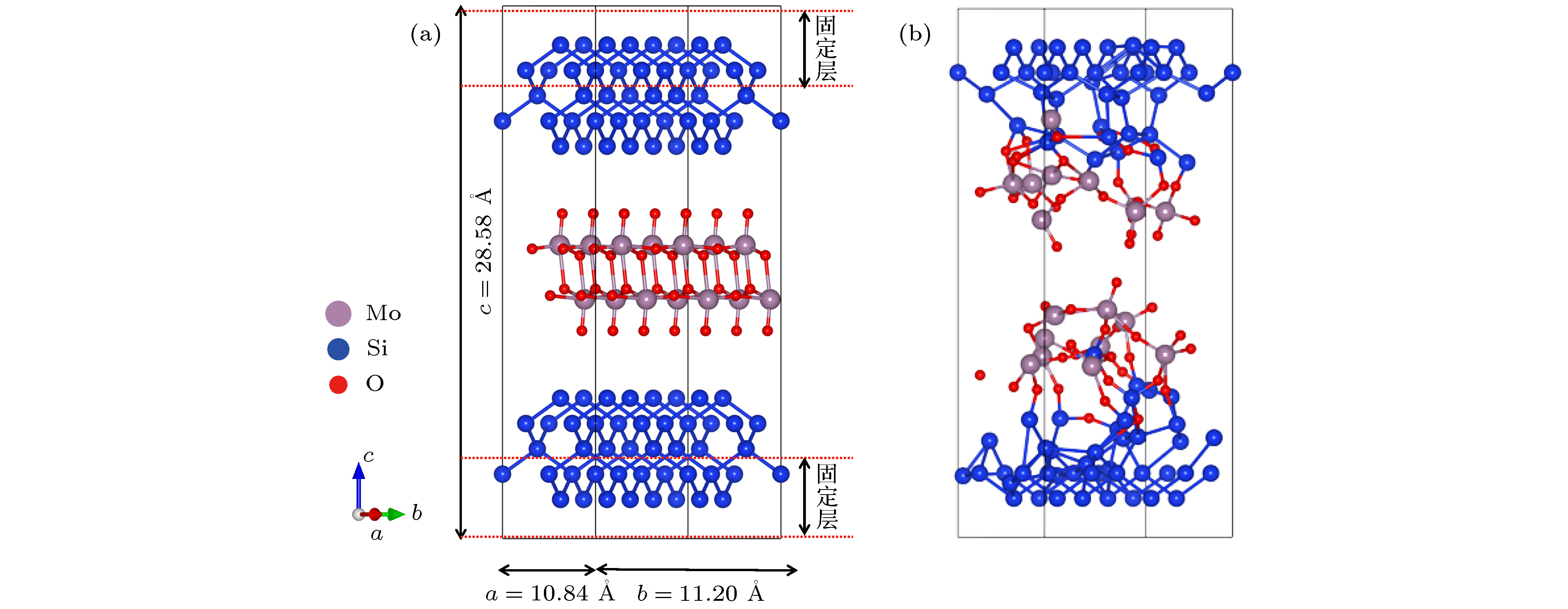
图 1 MoO3(010)/Si(100)分子动力学模型 (a)扩散反应前; (b)扩散反应后; 灰色球、蓝色球、红色球分别代表钼原子、硅原子和氧原子
Fig. 1. The structure model of MoO3(010)/Si(100) interface: (a) Before the ab initio molecular dynamics; (b) after the ab initio molecular dynamics. The grey, blue and red balls stand for Mo atoms, Si atoms, and O atoms, respectively
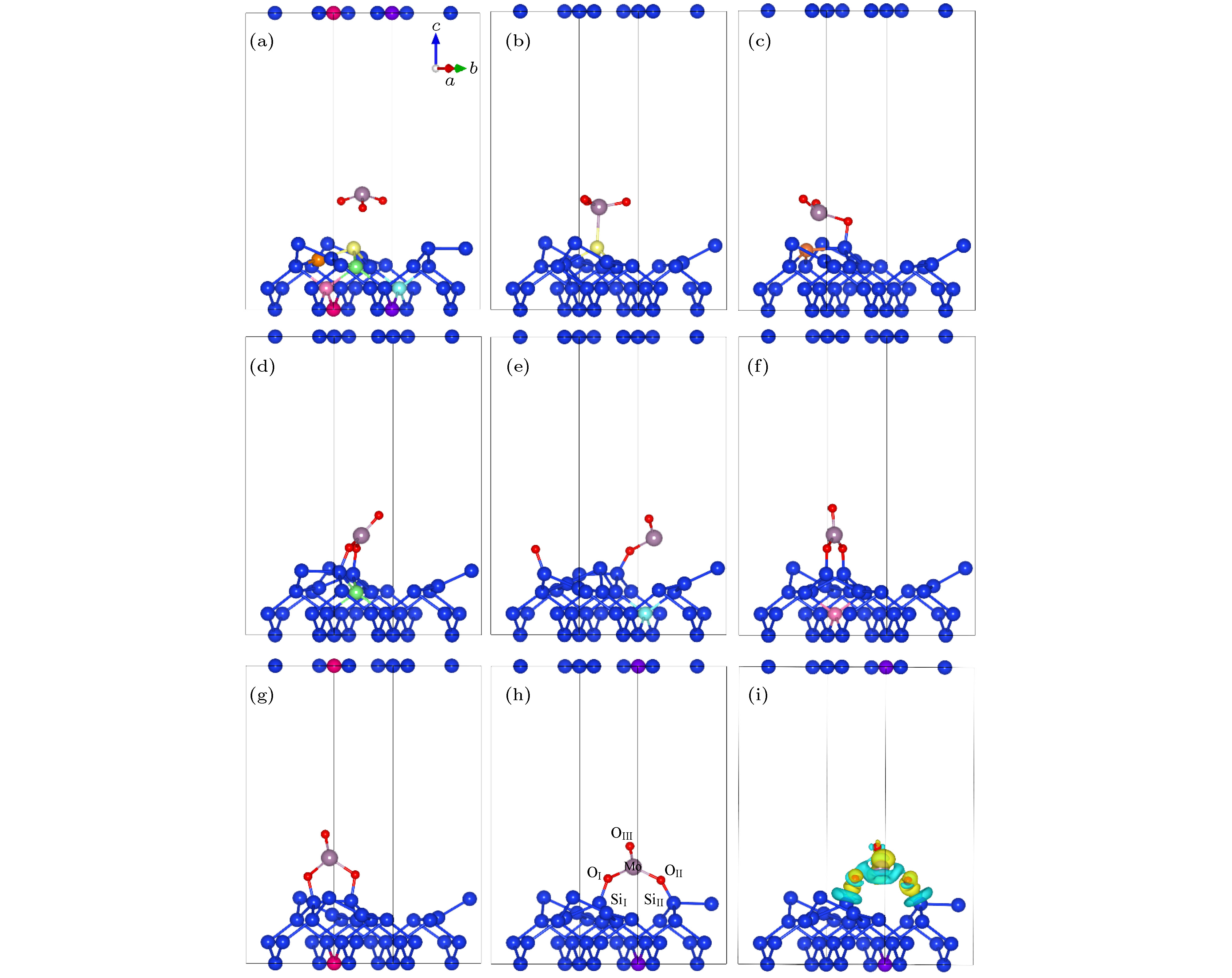
图 2 MoO3在Si(100)不同吸附位点的结构示意图 (a) MoO3分子结构及重构后Si(100)表面形貌; (b)−(h) MoO3在吸附位点1−7时优化后的吸附模型; (i)最佳吸附位点7的差分电荷密度(黄色和绿色表示得失电子)
Fig. 2. Adsorption configurations of MoO3 on Si (100) surface: (a) The optimized geometries of MoO3 molecule and reconstructed Si (100); (b)−(h) the adsorption configurations of MoO3 adsorbed on the different adsorption sites of Si (100) surface; (i) the difference charge density of MoO3 on the best adsorption site 7 of Si (100)

图 4 不同生长条件下替位杂质形成能 (a) Si替位Mo; (b) Mo替位Si; 黑线表示晶体硅的化学势, 红线表示富氧条件下硅的化学势
Fig. 4. The formation energy for the two substitutional defects: (a) Si in place of a Mo in MoO3; (b) Mo in place of a Si in SiO2. The black curves stand for the bulk Si chemical potential and the red curves stand for the chemical potential for Si in the SiO2 under an oxygen-rich environment
表 1 MoO3在Si(100)不同吸附位点的吸附能
Table 1. The adsorption energy of MoO3 on Si (100)
吸附位点 1 2 3 4 5 6 7 吸附能Eab/eV –2.36 –4.21 –5.35 –5.35 –5.19 –5.06 –5.36  下载: 导出CSV
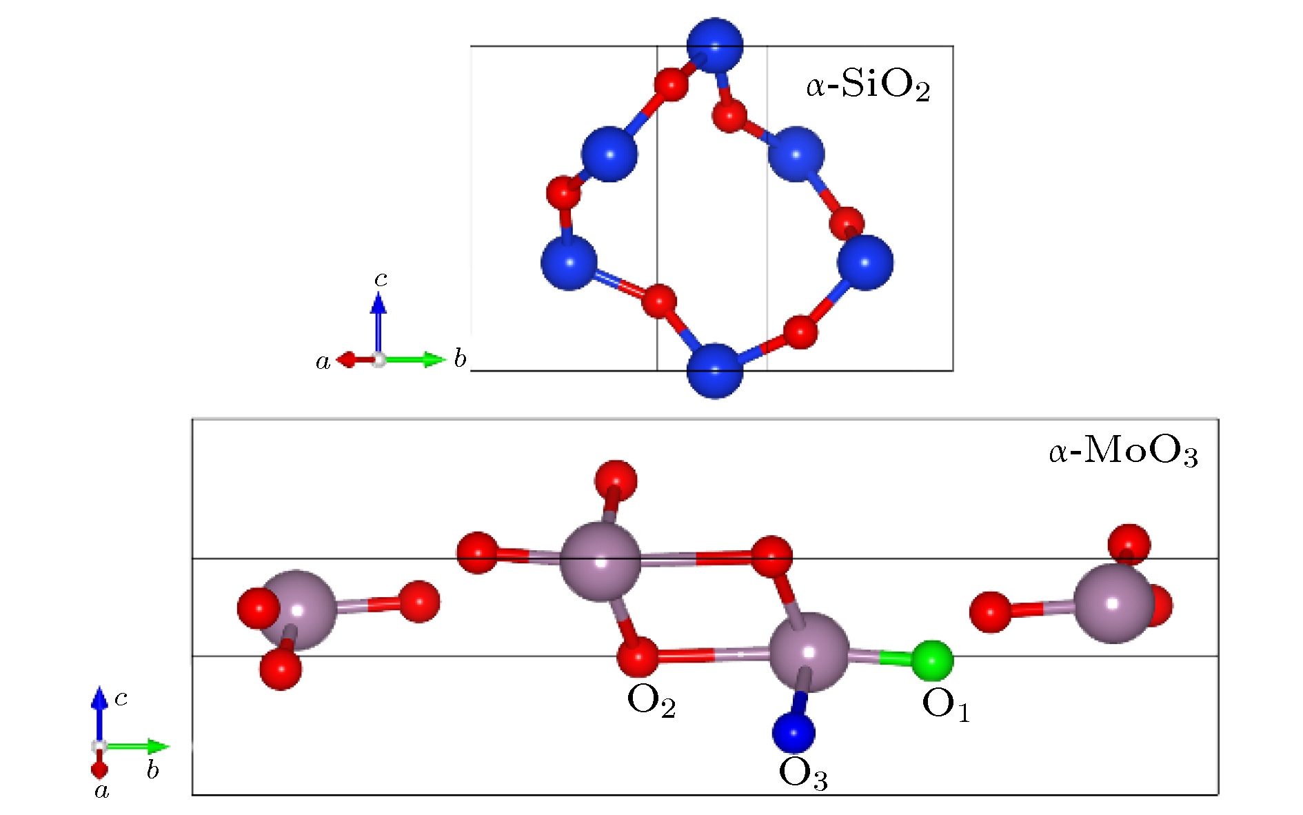
表 2 吸附前后体系7结构参数变化及Bader电荷
Table 2. The structure parameters and Bader charge of MoO3 adsorbed on the adsorption site 7 of Si (100) surface
结构参数 键长/Å 键角/(°) Mo—OI Mo—OΠ Mo—OШ OI —Mo— OΠ OΠ—Mo—OШ OШ—Mo—OI 吸附前 1.73 1.73 1.73 107.73 107.74 107.77 吸附后 1.95 1.94 1.71 125.62 116.92 116.11 Bader电荷/e SiI SiΠ Mo OI OΠ OШ 吸附前 3.88 3.98 3.91 6.72 6.67 6.71 吸附后 3.07 3.21 4.14 7.36 7.35 6.72
下载: 导出CSV
-
[1] Gerling L G, Mahato S, Morales-Vilches A, Masmitja G, Ortega P, Voz C, Alcubilla R, Puigdollers J 2016 Sol. Energy Mater. Sol. Cells 145 109
Google Scholar
[2] Bullock J, Cuevas A, Allen T, Battaglia C 2014 Appl. Phys. Lett. 105 232109
Google Scholar
[3] Battaglia C, Yin X T, Zheng M, Sharp I D, Chen T, McDonnell S, Azcatl A, Carraro C, Ma B W, Maboudian R, Wallace R M, Javey A 2014 Nano Lett. 14 967
Google Scholar
[4] Battaglia C, Nicolás S M D, Wolf S D, Yin X T, Zhang M, Ballif C, Javey A 2014 Appl. Phys. Lett. 104 113902
Google Scholar
[5] Geissbühler J, Werner J, Nicolas S M D, Barraud L, Hessler-Wyser A, Despeisse M, Nicolay S, Tomasi A, Niesen B, Wolf S D, Ballif C 2015 Appl. Phys. Lett. 107 081601
Google Scholar
[6] Gerling L G, Voz C, Alcubilla R, Puigdollers J 2016 J. Mater. Res. 32 260
[7] Gao M, Chen D Y, Han B C, Song W L, Zhou M, Song X M, Xu F, Zhao L, Li Y H, Ma Z Q 2018 ACS Appl. Mater. Interfaces 10 27454
Google Scholar
[8] Chen D Y, Gao M, Wan Y Z, Li Y H, Guo H B, Ma Z Q 2019 Appl. Surf. Sci. 473 20
Google Scholar
[9] Kresse K, Furthmüller J 1996 Phys. Rev. B 54 11169
Google Scholar
[10] Perdew J P, Burke K, Ernzerhof M 1996 Phys. Rev. Lett. 77 3865
Google Scholar
[11] Blöchl P E 1994 Phys. Rev. B 50 17953
Google Scholar
[12] Lambert D S, Murphy S T, Lennon A, Burr P A 2017 RSC Adv. 7 53810
Google Scholar
[13] Nosé S 1984 J. Chem. Phys. 81 511
[14] Fialko E F, Kikhtenko A V, Goncharov V B, Zamaraev K I 1997 J. Phys. Chem. A 101 8607
[15] Oliveira J A, Almeida W B D, Duarte H A 2003 Chem. Phys. Lett. 372 650
Google Scholar
[16] Anez R, Sierraalta A, Díaz L, Bastardo A, Coll D 2015 Appl. Surf. Sci. 335 160
Google Scholar
[17] Lu S Q, Wang C, Jin Y X, Bu Q Q, Yang Y 2012 J. Synthetic Crystals 41 1037
[18] Pavlova T V, Zhidomirov G M, Eltsov K N 2018 J. Phys. Chem. C 122 1741
[19] Wan Y Z, Gao M, Li Y, Du H W, Li Y H, Guo H B, Ma Z Q 2017 Appl. Phys. Lett. 110 213902
Google Scholar
[20] 陶鹏程, 黄燕, 周孝好, 陈效双, 陆卫 2017 物理学报 66 118201
Google Scholar
Tao P C, Huang Y, Zhou X H, Chen X S, Lu W 2017 Acta Phys. Sin. 66 118201
Google Scholar
[21] Coquet R, Willock D J 2005 Phys. Chem. Chem. Phys. 7 3819
Google Scholar
[22] Scopel W L, Silva A J R D, Orellana W, Fazzio A 2004 Appl. Phys. Lett. 84 1492
Google Scholar
[23] Liu H F, Yang R B, Yang W F, Jin Y J, Lee C J J 2018 Appl. Surf. Sci. 439 583
Google Scholar

 下载:
下载:
计量
- 文章访问数: 14592
- PDF下载量: 172
- 被引次数: 0
