


-
红外探测器具有把物体辐射的光子信息转换为电信号的能力, 拓宽了人们观察自然环境与人类活动的边界. 当前, 长波及甚长波红外探测器已在大气监测、夜间侦查、深空探测等领域有诸多应用. 随着各国对高端红外探测器要求的快速提升, 传统红外探测器难以兼顾高响应率、高响应速度以及多维探测等性能指标的瓶颈日益凸显. 基于微纳光学理论设计的人工微纳结构, 可实现其与红外光子的高效耦合, 综合调控红外光场的振幅、偏振、相位及波长等自由度. 为拓展红外探测器额外的调控自由度, 进而在实现高量子效率的同时, 兼顾较高的响应速率与优异的偏振或波长选择性, 集成红外探测器与人工微纳结构的研究思路近年来被广泛应用. 本文讨论了人工微纳结构在长波及甚长波红外探测领域的应用进展, 详述了表面等离激元、局域等离激元、谐振腔结构、陷光结构、超透镜、赝表面等离激元、间隙等离激元和声子极化激元等机制的应用现状及各机制固有的优劣势, 进而指出了人工微纳结构在长波及甚长波红外探测应用的发展前景与方向.The infrared detectors own the ability to convert information carried by photons radiated by objects into electrical signals, which broadens the horizons of human beings observing the natural environment and human activities. At present, long and very long-wavelength infrared detections have many applications in atmospheric monitoring, biological spectroscopy, night vision, etc. As the demand for high-performance infrared detectors grows rapidly, it is difficult for traditional infrared detectors to arrive at performance indicators such as high response rate, high response speed, and multi-dimensional detection. The artificial structure designed based on micro- and nano-optics can be coupled with infrared photons efficiently, and control the degrees of freedom of infrared light fields such as amplitude, polarization, phase, and wavelength comprehensively. The systems integrated by infrared detectors and artificial micro- and nano-photonic structures provide additional controllable degrees of freedom for infrared detectors. And they are expected to achieve high quantum efficiency and other merits such as high response rate, excellent polarization, and wavelength selectivity. In this review paper, the research progress of the application of artificial micro- and nano-structure in the long and very long-wavelength infrared bands is presented; the advantages, disadvantages, and the application status of different mechanisms are described in detail, which include surface plasmon polaritons, localized surface plasmon, resonant cavity structure, photon-trapping structure, metalens, spoof surface plasmon, gap plasmon, and phonon polariton. In addition, the development prospect and direction of artificial micro- and nano-structure in long-wave and very long-wave infrared devices are further pointed out.
-
Keywords:
- infrared detector /
- artificial micro- and nano-structure /
- long- and very-long-wavelength /
- plasmons
通信作者: 谢润章, xierunzhang@mail.sitp.ac.cn ; 王鹏, w_peng@mail.sitp.ac.cn ; 胡伟达, wdhu@mail.sitp.ac.cn
作者简介:


[1] Ycas G, Giorgetta F R, Baumann E, Coddington I, Herman D, Diddams S A, Newbury N R 2018 Nat. Photonics 12 202
 Google Scholar
[2] Norton P 2006 Opto-Electron. Rev. 14 1
Google Scholar
[3] Wu P, Ye L, Tong L, Wang P, Wang Y, Wang H, Ge H, Wang Z, Gu Y, Zhang K, Yu Y, Peng M, Wang F, Huang M, Zhou P, Hu W 2022 Light-Sci. Appl. 11 6
Google Scholar
[4] Rao G A, Mahulikar S P 2005 Aerosp. Sci. Technol. 9 701
Google Scholar
[5] For the James Webb Space Telescope (https://www.jwst.nasa.gov)
[6] Xin L 2022 The Innovation 3 100198
Google Scholar
[7] 胡伟达, 李庆, 陈效双, 陆卫 2019 物理学报 68 120701
Google Scholar
Hu W D, Li Q, Chen X S, Lu W 2019 Acta Physica Sinica 68 120701
Google Scholar
[8] Rogalski A, Antoszewski J, Faraone L 2009 J. Appl. Phys. 105 091101
Google Scholar
[9] Hu W D, Chen X S, Ye Z H, Feng A L, Yin F, Zhang B, Liao L, Lu W 2013 IEEE J. Sel. Top. Quantum Electron. 19 4100107
Google Scholar
[10] Jin Z, Janoschka D, Deng J, Ge L, Dreher P, Frank B, Hu G, Ni J, Yang Y, Li J, Yu C, Lei D, Li G, Xiao S, Mei S, Giessen H, zu Heringdorf F M, Qiu C W 2021 eLight 1 5
Google Scholar
[11] Xiong J, Wu S T 2021 eLight 1 3
Google Scholar
[12] Xie R, Wang P, Wang F, Chen X S, Lu W, Hu W D 2021 Opt. Lett. 46 1361
Google Scholar
[13] Li S Q, Xu X, Veetil R M, Valuckas V, Paniagua-Domínguez R, Kuznetsov A I 2019 Science 364 1087
Google Scholar
[14] Lin K T, Lin H, Jia B 2020 Nanophotonics 9 3135
Google Scholar
[15] Barnes W L, Dereux A, Ebbesen T W 2003 Nature 424 824
Google Scholar
[16] Hutter E, Fendler J H 2004 Adv. Mater. 16 1685
Google Scholar
[17] Farag A, Ubl M, Konzelmann A, Hentschel M, Giessen H 2019 Opt. Express 27 25012
Google Scholar
[18] Ge H, Xie R, Chen Y, Wang P, Li Q, Gu Y, Guo J, He J, Wang F, Hu W 2021 Opt. Express 29 22823
Google Scholar
[19] Schuster J, Bellotti E 2013 Opt. Express 21 14712
Google Scholar
[20] Chen W T, Zhu A Y, Sanjeev V, Khorasaninejad M, Shi Z, Lee E, Capasso F 2018 Nat. Nanotechnol. 13 220
Google Scholar
[21] Garcia-Vidal F J, Martín-Moreno L, Pendry J B 2005 J. Opt. A:Pure Appl. Opt. 7 S97
Google Scholar
[22] Bozhevolnyi S I, Jung J 2008 Opt. Express 16 2676
Google Scholar
[23] Huber A, Ocelic N, Kazantsev D, Hillenbrand R 2005 Appl. Phys. Lett. 87 081103
Google Scholar
[24] Nie X, Zhen H, Huang G, Yin Y, Li S, Chen P, Zhou X, Mei Y, Lu W 2020 Appl. Phys. Lett. 116 161107
Google Scholar
[25] 郭家祥, 谢润章, 王鹏, 张涛, 张坤, 王海露, 贺婷, 李庆, 王芳, 陈效双, 陆卫, 胡伟达 2022 红外与毫米波学报 41 40
Google Scholar
Guo J X, Xie R Z, Wang P, He T, Li Q, Wang F, Chen X S, Lu W, Hu W D 2022 J Infrared Millmeter Waves 41 40
Google Scholar
[26] Hu W, Ye Z, Liao L, Chen H, Chen L, Ding R, He L, Chen X, Lu W 2014 Opt. Lett. 39 5184
Google Scholar
[27] Wood R W 1902 Philos. Mag. 4 396
Google Scholar
[28] Fano U 1941 J. Opt. Soc. Am. 31 213
Google Scholar
[29] Maier S A 2007 Plasmonics: Fundamentals and Applications (New York: Springer) pp21–27, pp66–69
[30] Bhat R D R, Panoiu N C, Brueck S R J, Osgood R M 2008 Opt. Express 16 4588
Google Scholar
[31] Sefidmooye Azar N, Shrestha V R, Crozier K B 2019 Appl. Phys. Lett. 114 091108
Google Scholar
[32] Zhang Y, Meng D, Li X, Yu H, Lai J, Fan Z, Chen C 2018 Opt. Express 26 30862
Google Scholar
[33] Nordin L, Petluru P, Kamboj A, Muhowski A J, Wasserman D 2021 Optica 8 1545
Google Scholar
[34] Lee S C, Krishna S, Brueck S R J 2011 IEEE Photonics Technol. Lett. 23 935
Google Scholar
[35] Vaillancourt J, Mojaverian N, Lu X 2014 IEEE Photonics Technol. Lett. 26 745
Google Scholar
[36] Li X, Ye X, Li G, Yu F, Chen J, Zhao Z, Li Z, Chen X 2021 Opt. Mater. Express 11 1167
Google Scholar
[37] Zhou Y, Qin Z, Liang Z, Meng D, Xu H, Smith D R, Liu Y 2021 Light-Sci. Appl. 10 138
Google Scholar
[38] Zhan P, Wang Z L, Dong H, Sun J, Wu J, Wang H T, Zhu S N, Ming N B, Zi J 2006 Adv. Mater. 18 1612
Google Scholar
[39] Chu Y, Schonbrun E, Yang T, Crozier K B 2008 Appl. Phys. Lett. 93 181108
Google Scholar
[40] Miao J, Hu W, Jing Y, Luo W, Liao L, Pan A, Wu S, Cheng J, Chen X, Lu W 2015 Small 11 2392
Google Scholar
[41] Stewart J W, Vella J H, Li W, Fan S, Mikkelsen M H 2020 Nat. Mater. 19 158
Google Scholar
[42] Fang Z, Wang Y, Schlather A E, Liu Z, Ajayan P M, García de Abajo F J, Nordlander P, Zhu X, Halas N J 2014 Nano Lett. 14 299
Google Scholar
[43] Tang X, Wu G f, Lai K W C 2017 J. Mater. Chem. C 5 362
Google Scholar
[44] Safaei A, Chandra S, Leuenberger M N, Chanda D 2019 ACS Nano 13 421
Google Scholar
[45] Guo Q, Yu R, Li C, Yuan S, Deng B, García de Abajo F J, Xia F 2018 Nat. Mater. 17 986
Google Scholar
[46] Suen J Y, Fan K, Montoya J, Bingham C, Stenger V, Sriram S, Padilla W J 2017 Optica 4 276
Google Scholar
[47] Shabbir M W, Chandra S, Leuenberger M N 2021 arXiv: 2103.10311
[48] Rogalski A 2012 Opto-Electron. Rev. 20 279
Google Scholar
[49] Levine B F 1993 J. Appl. Phys. 74 R1
Google Scholar
[50] Schneider H, Liu H C 2007 Quantum Well Infrared Photodetectors (New York: Springer) pp13–36
[51] Li Q, Li Z, Li N, Chen X, Chen P, Shen X, Lu W 2014 Sci. Rep. 4 6332
Google Scholar
[52] Cakmakyapan S, Lu P K, Navabi A, Jarrahi M 2018 Light-Sci. Appl. 7 20
Google Scholar
[53] Letka V, Bainbridge A, Craig A P, Al-Saymari F, Marshall A R J 2019 Opt. Express 27 23970
Google Scholar
[54] Deotare P B, McCutcheon M W, Frank I W, Khan M, Lončar M 2009 Appl. Phys. Lett. 94 121106
Google Scholar
[55] Goldflam M D, Kadlec E A, Olson B V, Klem J F, Hawkins S D, Parameswaran S, Coon W T, Keeler G A, Fortune T R, Tauke-Pedretti A, Wendt J R, Shaner E A, Davids P S, Kim J K, Peters D W 2016 Appl. Phys. Lett. 109 251103
Google Scholar
[56] Wang S, Yoon N, Kamboj A, Petluru P, Zheng W, Wasserman D 2018 Appl. Phys. Lett. 112 091104
Google Scholar
[57] Law S, Roberts C, Kilpatrick T, Yu L, Ribaudo T, Shaner E A, Podolskiy V, Wasserman D 2014 Phys. Rev. Lett. 112 017401
Google Scholar
[58] Zhou Y W, Li Z F, Zhou J, Li N, Zhou X H, Chen P P, Zheng Y L, Chen X S, Lu W 2018 Sci. Rep. 8 15070
Google Scholar
[59] Zhen T, Zhou J, Li Z, Chen X 2019 Adv. Opt. Mater. 7 1801627
Google Scholar
[60] Qu C, Ma S, Hao J, Qiu M, Li X, Xiao S, Miao Z, Dai N, He Q, Sun S, Zhou L 2015 Phys. Rev. Lett. 115 235503
Google Scholar
[61] Rogalski A, Martyniuk P, Kopytko M 2016 Rep. Prog. Phys. 79 046501
Google Scholar
[62] Li J, Li J, Zhou H, Zhang G, Liu H, Wang S, Yi F 2021 Opt. Express 29 22907
Google Scholar
[63] Jing Y, Li Z, Li Q, Chen P, Zhou X, Wang H, Li N, Lu W 2016 AIP Adv. 6 045205
Google Scholar
[64] Jing Y L, Li Z F, Li Q, Chen X S, Chen P P, Wang H, Li M Y, Li N, Lu W 2016 Sci. Rep. 6 25849
Google Scholar
[65] Zhou Y, Li Z, Zhou X, Zhou J, Zheng Y, Li L, Li N, Chen P, Chen X, Lu W 2019 Appl. Phys. Lett. 114 061104
Google Scholar
[66] Montoya J A, Tian Z-B, Krishna S, Padilla W J 2017 Opt. Express 25 23343
Google Scholar
[67] Yablonovitch E 1987 Phys. Rev. Lett. 58 2059
Google Scholar
[68] John S 1987 Phys. Rev. Lett. 58 2486
Google Scholar
[69] John S 1991 Phys. Today 44 32
Google Scholar
[70] Wang L G, Zhu S Y 2010 Phys. Rev. B 81 205444
Google Scholar
[71] Gao Y, Cansizoglu H, Polat K G, et al. 2017 Nat. Photonics 11 301
Google Scholar
[72] Cansizoglu H, Bartolo-Perez C, Gao Y, Ponizovskaya Devine E, Ghandiparsi S, Polat K G, Mamtaz H H, Yamada T, Elrefaie A F, Wang S Y, Islam M S 2018 Photonics Res. 6 734
Google Scholar
[73] Zhou H, Xu S, Lin Y, Huang Y C, Son B, Chen Q, Guo X, Lee K H, Goh S C K, Gong X, Tan C S 2020 Opt. Express 28 10280
Google Scholar
[74] Hu W D, Chen X S, Ye Z H, Lu W 2011 Appl. Phys. Lett. 99 091101
Google Scholar
[75] Liang J, Hu W, Ye Z, Liao L, Li Z, Chen X, Lu W 2014 J. Appl. Phys. 115 184504
Google Scholar
[76] Rabiee-Golgir H, Ghandiparsi S, Devine E P, et al. 2019 Infrared Technology and Applications XLV. 11002 110020T
Google Scholar
[77] Bomzon Z E, Biener G, Kleiner V, Hasman E 2002 Opt. Lett. 27 1141
Google Scholar
[78] Berry M V 1984 Proc. R. Soc. London, Ser. A 392 45
Google Scholar
[79] Khorasaninejad M, Chen Wei T, Devlin Robert C, Oh J, Zhu Alexander Y, Capasso F 2016 Science 352 1190
Google Scholar
[80] Uenoyama S, Ota R 2021 ACS Photonics 8 1548
Google Scholar
[81] Zhang S, Soibel A, Keo S A, Wilson D, Rafol S B, Ting D Z, She A, Gunapala S D, Capasso F 2018 Appl. Phys. Lett. 113 111104
Google Scholar
[82] Ning Y, Zhang S, Hu Y, Hao Q, Tang X 2020 Coatings 10 1218
Google Scholar
[83] Wenger T, Muller R, Wilson D, Gunapala S D, Soibel A 2021 AIP Adv. 11 085221
Google Scholar
[84] Hou H, Zhang Y, Luo Z, Zhang P, Zhao Y 2022 Opt Lasers Eng 150 106849
Google Scholar
[85] Mousavi S H, Khanikaev A B, Neuner B, Avitzour Y, Korobkin D, Ferro G, Shvets G 2010 Phys. Rev. Lett. 105 176803
Google Scholar
[86] Chang C C, Sharma Y D, Kim Y S, Bur J A, Shenoi R V, Krishna S, Huang D, Lin S Y 2010 Nano Lett. 10 1704
Google Scholar
[87] Ogawa S, Komoda J, Masuda K, Kimata M 2013 Opt. Eng. 52 127104
Google Scholar
[88] Zhao F, Zhang C, Chang H, Hu X 2014 Plasmonics 9 1397
Google Scholar
[89] Liu L, Chen Y, Huang Z, Du W, Zhan P, Wang Z 2016 Sci. Rep. 6 30414
Google Scholar
[90] Wu Z Q, Yang J L, Manjunath N K, Zhang Y J, Feng S R, Lu Y H, Wu J H, Zhao W W, Qiu C Y, Li J F, Lin S S 2018 Adv. Mater. 30 1706527
Google Scholar
[91] Schnell M, Alonso-González P, Arzubiaga L, Casanova F, Hueso L E, Chuvilin A, Hillenbrand R 2011 Nat. Photonics 5 283
Google Scholar
[92] Korobkin D, Urzhumov Y A, Neuner-Iii B, Zorman C, Zhang Z, Mayergoyz I D, Shvets G 2007 Appl. Phys. A 88 605
Google Scholar
[93] Hajian H, Ghobadi A, Butun B, Ozbay E 2018 Opt. Express 26 16940
Google Scholar
-
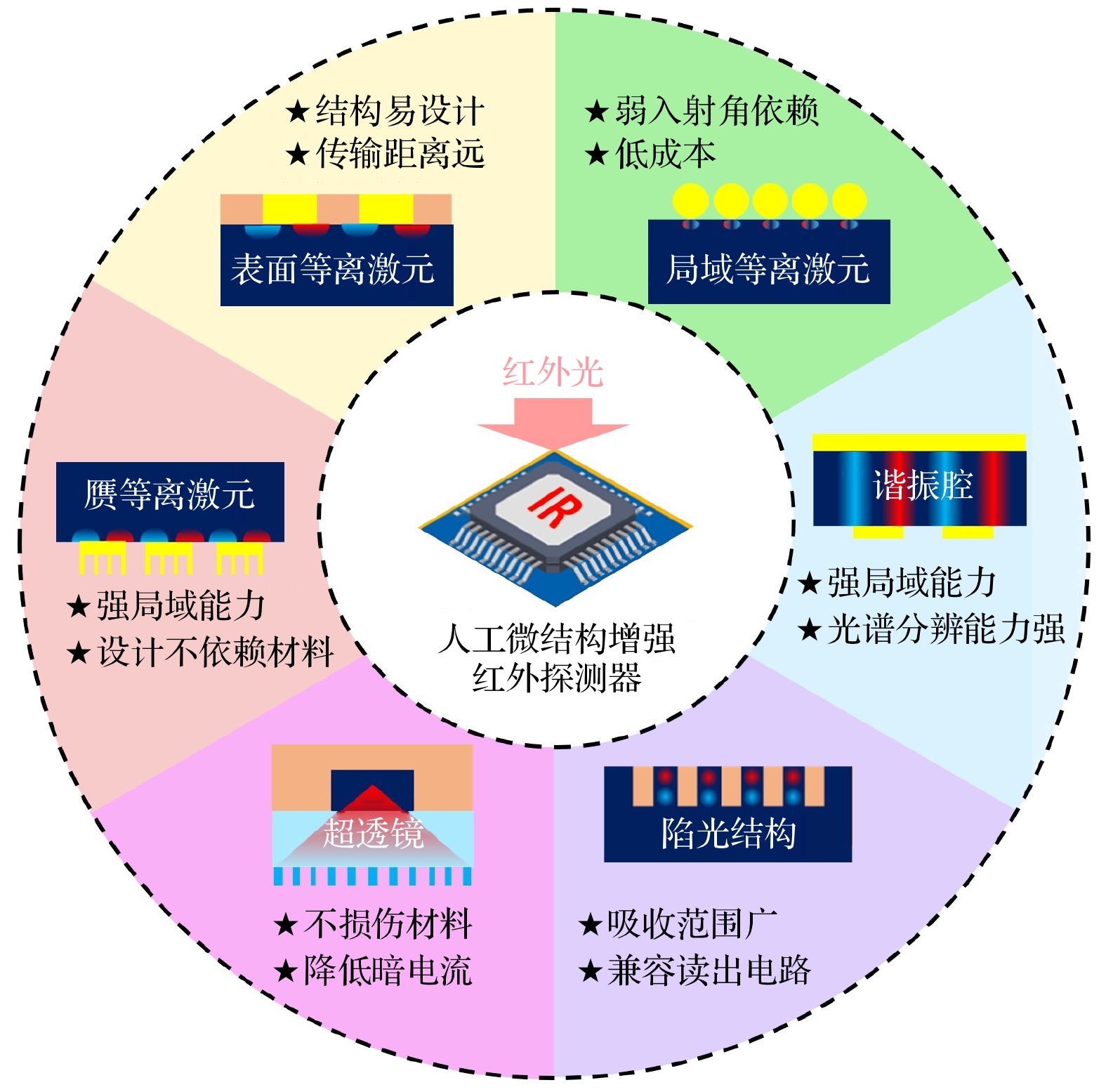
图 1 人工微纳结构增强长波及甚长波红外探测器的几种主要机制及特点
Fig. 1. Major mechanisms and main features of artificial micro- and nano-structures for long- and very-long-wavelength infrared detector enhancement.
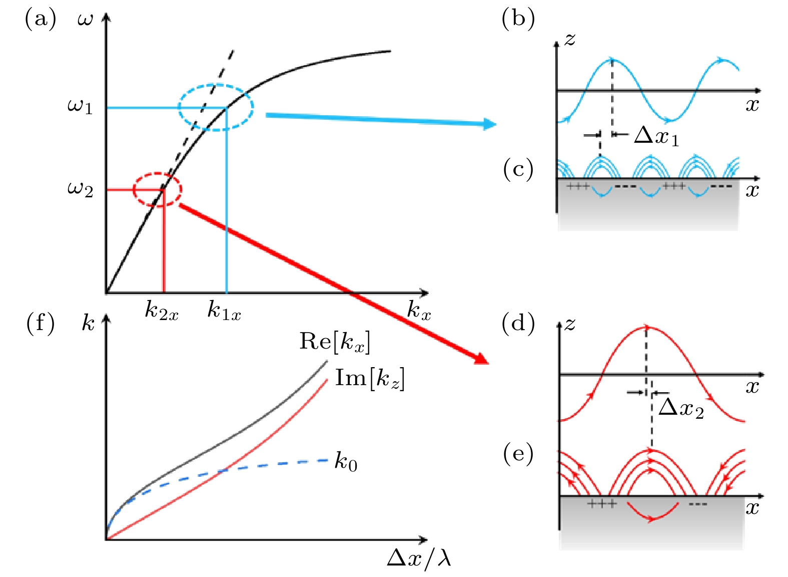
图 2 (a) SPP与介质中传输模的色散关系, k1x和k2x分别表示在SPP色散曲线在频率ω1(可见光波段)与ω2(红外光波段)处的水平波矢; (b) 频率ω1处, 传输模在介质中沿着x方向传播的电场示意图; (c) 频率ω1处SPP模式的电场示意图; (d) 频率ω2处, 传输模在介质中沿着x方向传播的电场示意图; (e) 频率ω2处, SPP模式在界面处的电场示意图; (f) Re[kx] 和Im[kz] 曲线示意图
Fig. 2. (a) Dispersion relation of SPP and propagation mode in the dielectric, k1x and k2x are the wave vector along the x-direction at frequency ω1 and ω2 on the SPP dispersion curve, respectively; (b) illustration of electric field of propagation mode in the dielectric along the x-direction at frequency ω1; (c) illustration of electric field of SPP mode at frequency ω1; (d) illustration of electric field of propagation mode in dielectric along the x-direction at frequency ω2; (e) illustration of electric field of SPP mode at frequency ω2; (f) schematic of relationship curves of Re[kx] and Im[kz].
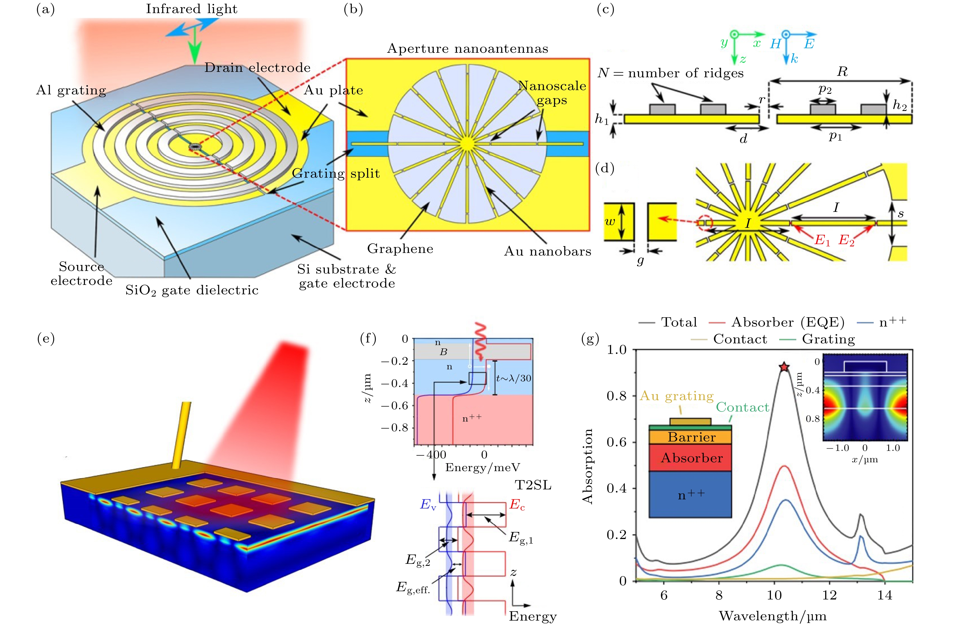
图 3 (a) 混合等离激元结构的石墨烯红外探测器示意图[31]; (b) 小孔纳米天线放大图[31]; (c) 光栅结构示意图; (d) 纳米天线和狭缝示意图[31]; (e) SPP增强超薄二类超晶格探测器示意图[33]; (f) 顶部为势垒阻挡型超薄红外探测器, 底部为二类超晶格能带结构[33]; (g) 探测器及其中不同材料的吸收谱, 插图为 |Hy| 在光电探测器内分布[33]
Fig. 3. (a) Schematic of graphene infrared detector with a hybrid plasmonic structure[31]; (b) details of the aperture nanoantenna[31]; (c) schematic of grating structure[31]; (d) schematic of nanoantenna and slit[31]; (e) schematic of SPP enhanced ultrathin type-II superlattice detector[33]; (f) top: nBn ultra-thin infrared detectors, bottom: band structure of type-II superlattices[33]; (g) absorption spectrums of the detector and the respective material layers in the detector. Inset shows the |Hy| distribution of the detector[33].


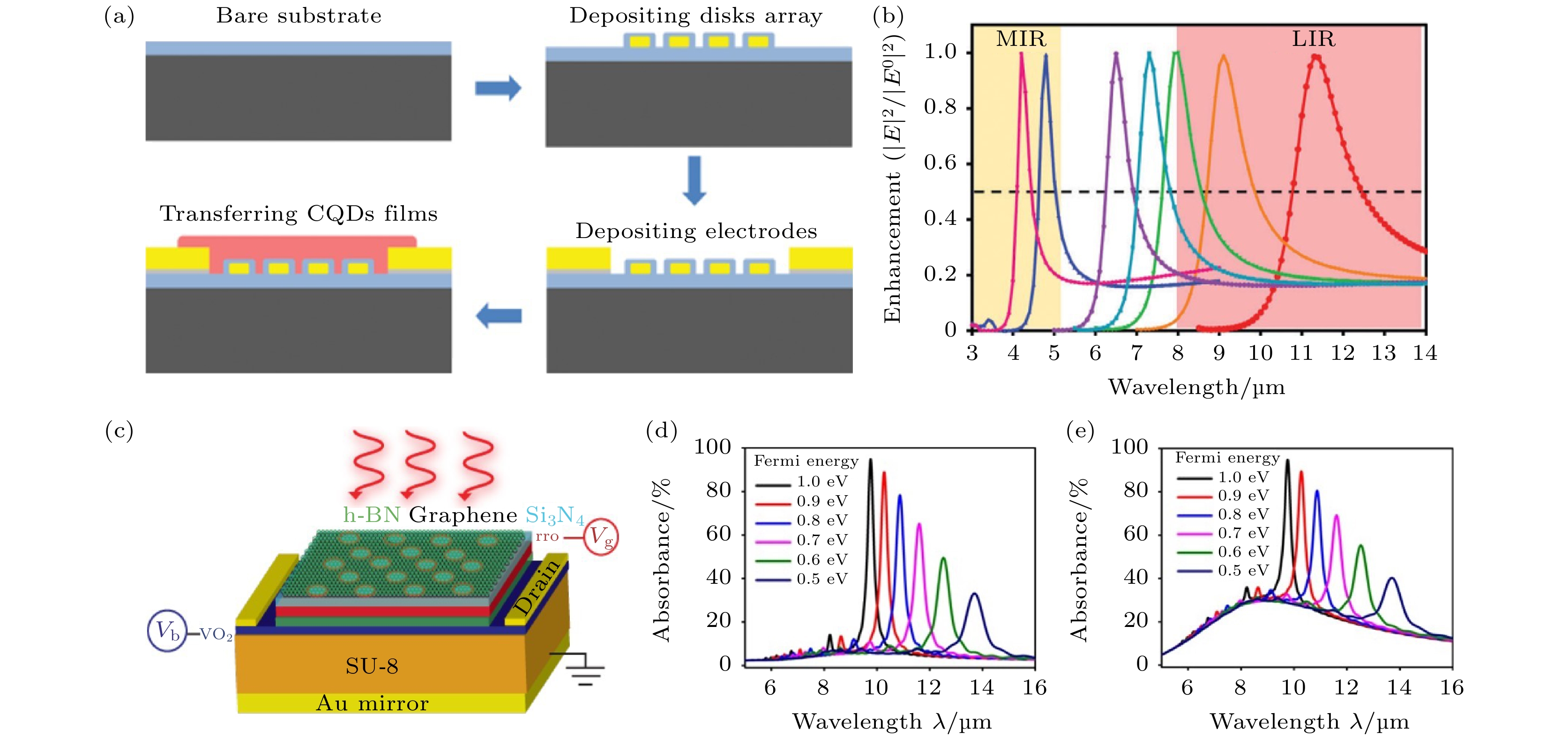
图 6 (a) 带有金等离激元结构的HgSe量子点探测器制备方法[43]; (b) 不同等离激元圆盘阵列半径下的增强比[43]; (c) 石墨烯与氧化钒异质结构红外探测器示意图[47]; (d) 氧化钒为绝缘相时, 不同费米能级的石墨烯探测器吸收谱[47]; (e) 氧化钒为金属相时, 不同费米能级的石墨烯探测器吸收谱[47]
Fig. 6. (a) Preparation methodology of the HgSe quantum dot detector with Au plasmonic structures[43]; (b) enhancement of different plasmonic disk arrays with different radius[43]; (c) schematic of graphene-HfO2 heterostructure infrared detector[47]; (d) absorption spectrum of the graphene detectors at different Fermi levels when vanadium dioxide is in its insulating phase[47]; (e) absorption spectrum of the graphene detectors at different Fermi levels when vanadium dioxide is in its metallic phase[47].
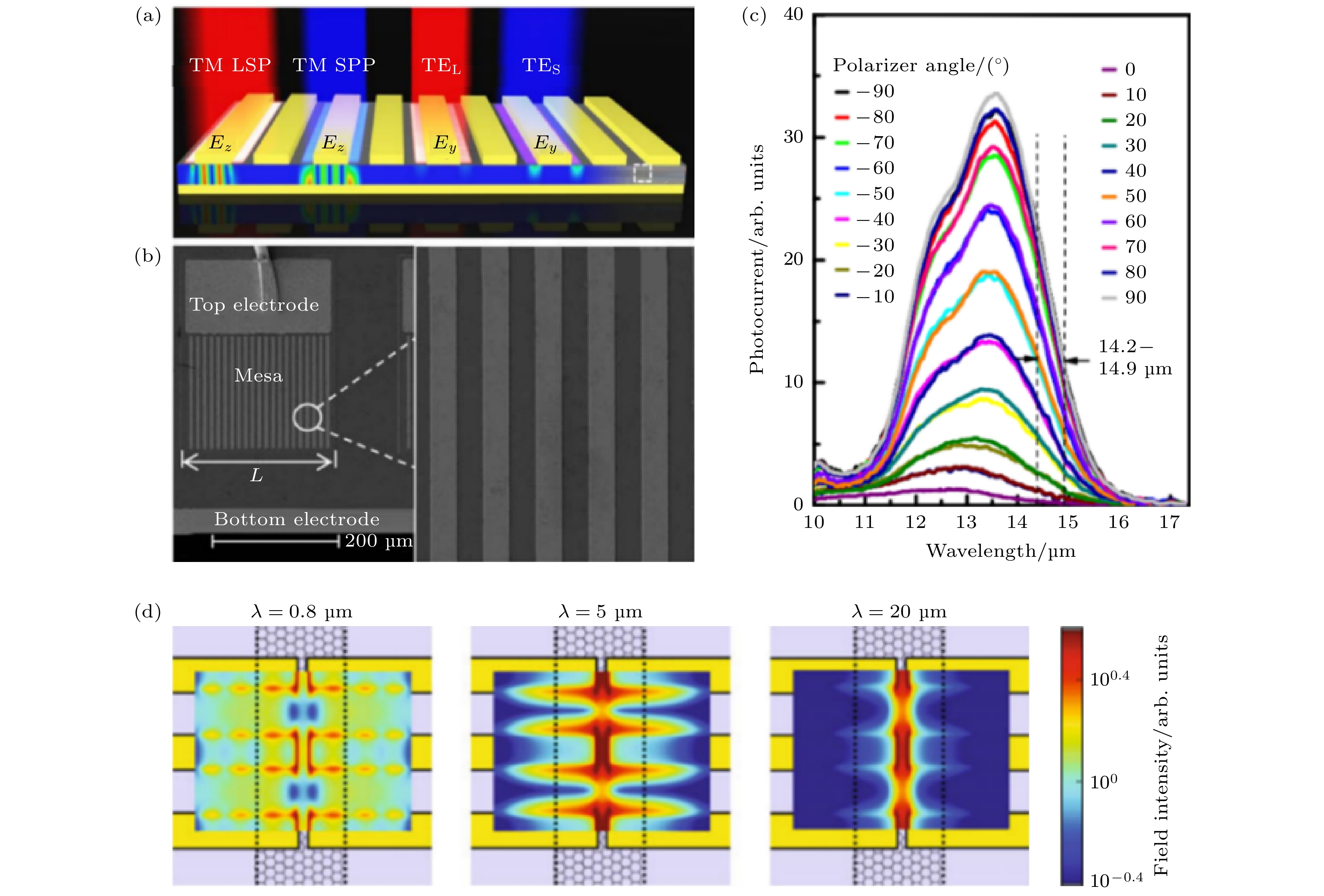
图 7 (a) TM和TE偏振光的不同耦合行为[51]; (b) 量子阱探测器的扫描电镜图像[51]; (c) 不同偏振角度下量子阱探测器的光电流谱[51]; (d) 光偏振垂直于石墨烯纳米带下, 波长0.8, 5和20 μm时的场强分布[52]
Fig. 7. (a) Different coupling behavior of TM and TE polarized light[51]; (b) scanning electron microscopy image of the quantum well detector[51]; (c) photocurrent spectrum of the quantum well detector under different polarization angles[51]; (d) field intensity distribution of 0.8, 5, and 20 μm when light polarization perpendicular to graphene nanostrips[52].

图 8 (a) 优化前的等离激元微腔结构中金属和量子阱吸收谱[59]; (b) 优化后的等离激元微腔结构中金属和量子阱吸收谱[59]; (c) 金属微腔量子阱示意图[24]
Fig. 8. (a) Absorption spectra of metals and quantum wells in plasmonic microcavity structures before optimization[59]; (b) absorption spectra of metals and quantum wells in plasmonic microcavity structures after optimization[59]; (c) schematic of metal microcavity quantum well[24].

图 9 (a) MIM量子阱探测器示意图[63]; (b) MIM量子阱探测器和45°耦合的标准量子阱探测器响应谱[63]; (c) 光学方法拓展截止波长的实验值(黑色)和改变材料参数拓展截止波长的计算值(红色)[65]; (d) MIM微腔结构制备流程图[66]
Fig. 9. (a) Schematic of MIM quantum well detector[63]; (b) responsivity spectrum of MIM and standard 45° coupled quantum well detector[63]; (c) experiment value (black) of optical method and the calculated value (red) of change material parameters traditional method to extend cut-off wavelength[65]; (d) flow chart of fabrication of MIM microcavity structure[66].
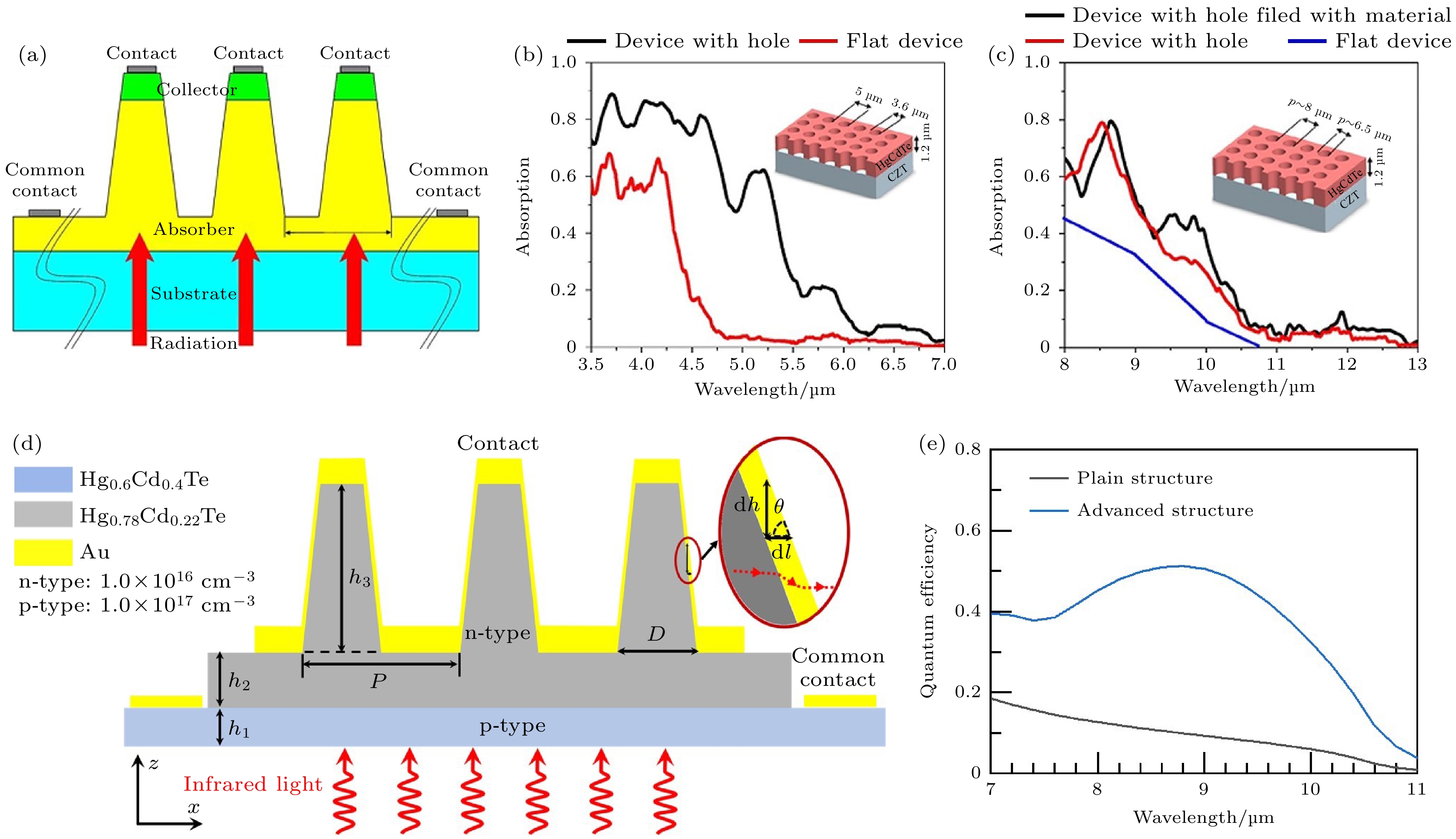
图 10 (a) 碲镉汞陷光结构红外探测器示意图[75]; (b) 中波红外碲镉汞平面结构和陷光结构探测器吸收谱[76]; (c) 长波红外碲镉汞平面结构探测器、无填充介质陷光结构探测器和填充介质陷光结构探测器吸收谱[76]; (d) 基于金属薄膜横向的趋肤传输模式增强碲镉汞探测器吸收示意图[18]; (e) 碲镉汞平面结构、碲镉汞横向传输模式增强的改进结构在7—11 μm的量子效率[18]
Fig. 10. (a) Schematic of the HgCdTe photon-trapping structure infrared detector[75]; (b) absorption spectrum of mid-wavelength infrared HgCdTe plain structure detector and photon-trapping structure detector[76]; (c) absorption spectrum of long-wavelength infrared HgCdTe plain detector, without dielectric-filled photon-trapping structure detector, and dielectric-filled photon-trapping structure detector[76]; (d) schematic of enhanced absorption of HgCdTe detector based on metal thin film horizontal skin propagation mode[18]; (e) quantum efficiencies of HgCdTe plain structure and HgCdTe advanced structure with lateral transmission mode enhancement at 7–11 μm[18].
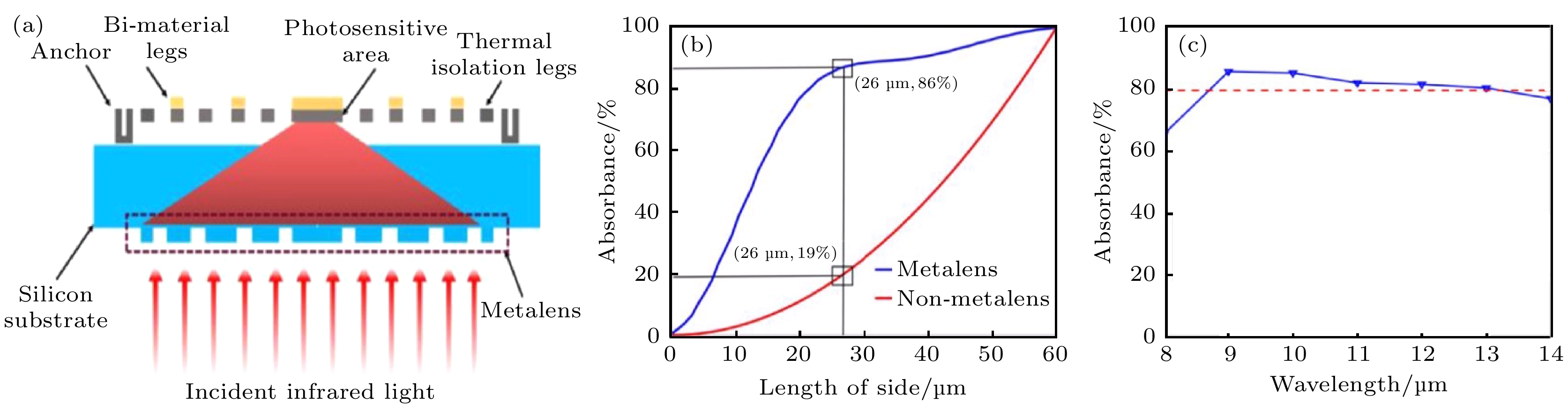
图 11 (a) 超透镜集成的长波红外探测器示意图[84]; (b) 有无超透镜结构的长波红外探测在不同光敏面积下的吸收比[84]; (c) 超透镜长波红外探测器在8—14 μm吸收谱[84]
Fig. 11. (a) Schematic of metalens integrate with long-wavelength infrared detector[84]; (b) absorptance of long-wavelength infrared detectors with and without metalens under different photosensitive areas[84]; (c) absorptance of infrared detectors with metalens at 8–14 μm[84].

图 12 (a) 完美电导体表面的一维凹槽阵列示意图, 凹槽参数为宽度a、厚度h和周期 d [21]; (b) 各向异性的有效介质代替凹槽阵列的示意图[21]; (c) a/d = 0.2和h/d = 1时所激发的表面束缚波的色散关系[86]; (d) 二维金属小孔阵列增强量子阱探测器示意图[86]; (e) 有二维金属小孔阵列和无二维金属小孔阵列量子点红外探测器红外响应[86]; (f) 9.39 μm处小孔附近的电场分布[86]
Fig. 12. (a) Schematic of a one-dimensional groove array on the surface of a perfect electrical conductor, the groove parameter is width a, depth h and period d[21]; (b) schematic illustration that replaces the groove array by the anisotropic effective dielectric layer[21]; (c) dispersion relation of excited surface bound wave when a/d = 0.2 and h/d = 1[86]; (d) schematic of a two-dimensional metal hole array enhanced quantum well detector[86]; (e) infrared response of quantum dot infrared detectors with and without two-dimensional metal hole arrays[86]; (f) electric field distribution near the hole at 9.39 μm[86].
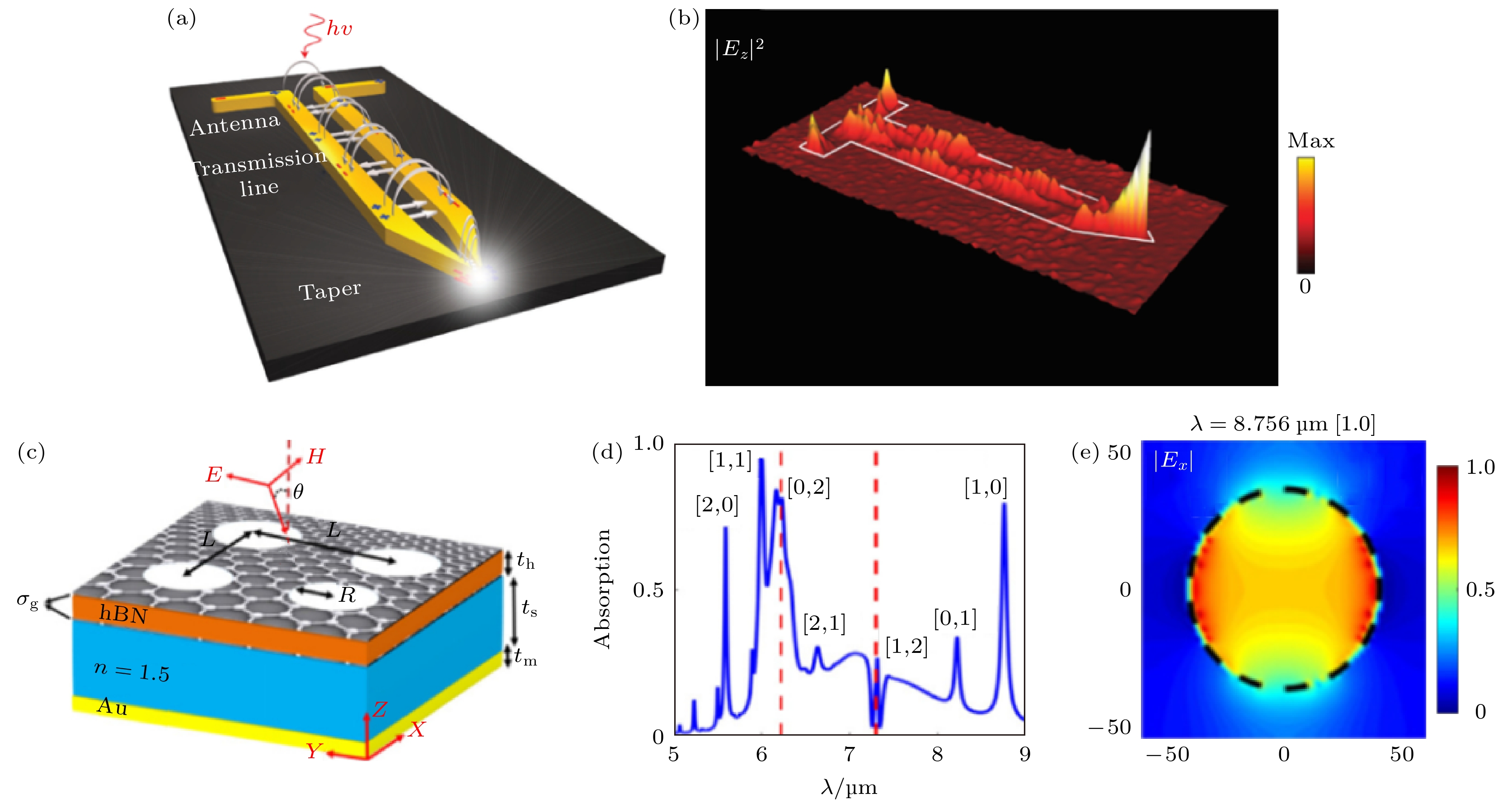
图 13 (a) 锥形天线聚焦红外光场的示意图[91]; (b) 近场成像显示的电场|Ez|2分布[91]; (c) 带有正方形小孔阵列的石墨烯/氮化硼/石墨烯多层结构示意图[93]; (d) 石墨烯/氮化硼/石墨烯多层结构吸收谱[93]; (e) 模式[1, 0]处的面内电场分布[93]
Fig. 13. (a) Schematic of tapered antenna focusing infrared light field[91]; (b) near-field image showing electric field |Ez|2 distribution[91]; (c) schematic of graphene/hBN/graphene multilayer structure with square hole array[93]; (d) absorption spectrum of graphene/hBN/graphene multilayer structure[93]; (e) in-plane electric field distribution at mode [1, 0][93].
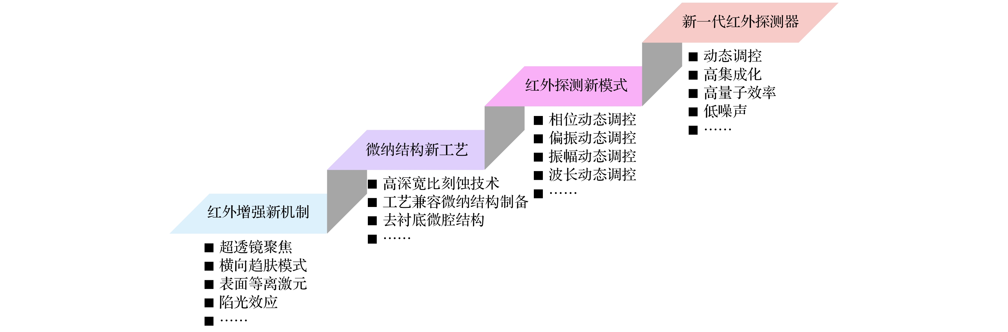
图 14 人工微纳结构与红外探测器高度集成化的新一代红外探测器发展展望
Fig. 14. Development prospect of the new generation of infrared detectors with high-integration of artificial micro- and nano-structures and infrared detectors.
表 1 不同增强的机制在长波及甚长波红外波段的代表性工作
Table 1. Representative work of different enhancement mechanisms in long and very long-wavelength infrared bands.
增强机制 红外材料 结构类型 器件增强倍率 材料吸收率 规模 其他特性 文献 表面
等离激元— 牛眼结构 436
(10.2 μm吸收率)— 单元 信噪比提高5.2 [30] 石墨烯 牛眼结构与纳米狭缝 558
(10.84 μm吸收率)0.3595%
(10.84 μm)单元 探测率增强31.8 [31] 二类超晶格 光栅结构 13.5
(10.4 μm光响应)50%
(10.4 μm)单元 高温工作
195 K[33] 量子点 金属小孔阵列 — — 阵列 NEDT提高50% [35] 局域
等离激元石墨烯 圆盘阵列 10
(12.4 μm吸收率)32%
(12.4 μm)单元 吸收峰动态调节 [42] 量子点 圆盘阵列 2.08
(9 μm 光响应)— 单元 — [43] 石墨烯 小孔阵列 — — 单元 热响应时间
1 ms[47] 量子阱 金属光栅 6
(14.7 μm 光响应)— 阵列 偏振比
65[51] 谐振腔 量子阱 金属光栅/谐振腔 — — 阵列 偏振比
136[58] 量子阱 金属阵列/谐振腔 — 82%
(12.5 μm)阵列 低热损耗 [59] 量子阱 金属微腔 — 阵列 偏振和波长选择 [24] 陷光结构 碲镉汞 柱状阵列 — 80%
(8 μm)阵列 — [75] 碲镉汞 小孔阵列 5.8
(10 μm吸收率)58%
(10 μm)单元 — [76] 碲镉汞 柱状阵列 7.9
(9 μm 量子效率)55%
(9 μm)阵列 小周期、串扰低 [18] 超透镜 — 超表面 — 86%
(10 μm)阵列 8—14 μm
平均收集效率80%[84] 赝等离激元 量子点 小孔阵列 1.3
(8.8 μm 光响应)10%
(8.8 μm)单元 — [86] 量子阱 金属阵列/金属反射层 33
(14.4 μm 吸收率)62%
(14.5 μm)单元 宽角度耦合 [89]  下载: 导出CSV
-
[1] Ycas G, Giorgetta F R, Baumann E, Coddington I, Herman D, Diddams S A, Newbury N R 2018 Nat. Photonics 12 202
Google Scholar
[2] Norton P 2006 Opto-Electron. Rev. 14 1
Google Scholar
[3] Wu P, Ye L, Tong L, Wang P, Wang Y, Wang H, Ge H, Wang Z, Gu Y, Zhang K, Yu Y, Peng M, Wang F, Huang M, Zhou P, Hu W 2022 Light-Sci. Appl. 11 6
Google Scholar
[4] Rao G A, Mahulikar S P 2005 Aerosp. Sci. Technol. 9 701
Google Scholar
[5] For the James Webb Space Telescope (https://www.jwst.nasa.gov)
[6] Xin L 2022 The Innovation 3 100198
Google Scholar
[7] 胡伟达, 李庆, 陈效双, 陆卫 2019 物理学报 68 120701
Google Scholar
Hu W D, Li Q, Chen X S, Lu W 2019 Acta Physica Sinica 68 120701
Google Scholar
[8] Rogalski A, Antoszewski J, Faraone L 2009 J. Appl. Phys. 105 091101
Google Scholar
[9] Hu W D, Chen X S, Ye Z H, Feng A L, Yin F, Zhang B, Liao L, Lu W 2013 IEEE J. Sel. Top. Quantum Electron. 19 4100107
Google Scholar
[10] Jin Z, Janoschka D, Deng J, Ge L, Dreher P, Frank B, Hu G, Ni J, Yang Y, Li J, Yu C, Lei D, Li G, Xiao S, Mei S, Giessen H, zu Heringdorf F M, Qiu C W 2021 eLight 1 5
Google Scholar
[11] Xiong J, Wu S T 2021 eLight 1 3
Google Scholar
[12] Xie R, Wang P, Wang F, Chen X S, Lu W, Hu W D 2021 Opt. Lett. 46 1361
Google Scholar
[13] Li S Q, Xu X, Veetil R M, Valuckas V, Paniagua-Domínguez R, Kuznetsov A I 2019 Science 364 1087
Google Scholar
[14] Lin K T, Lin H, Jia B 2020 Nanophotonics 9 3135
Google Scholar
[15] Barnes W L, Dereux A, Ebbesen T W 2003 Nature 424 824
Google Scholar
[16] Hutter E, Fendler J H 2004 Adv. Mater. 16 1685
Google Scholar
[17] Farag A, Ubl M, Konzelmann A, Hentschel M, Giessen H 2019 Opt. Express 27 25012
Google Scholar
[18] Ge H, Xie R, Chen Y, Wang P, Li Q, Gu Y, Guo J, He J, Wang F, Hu W 2021 Opt. Express 29 22823
Google Scholar
[19] Schuster J, Bellotti E 2013 Opt. Express 21 14712
Google Scholar
[20] Chen W T, Zhu A Y, Sanjeev V, Khorasaninejad M, Shi Z, Lee E, Capasso F 2018 Nat. Nanotechnol. 13 220
Google Scholar
[21] Garcia-Vidal F J, Martín-Moreno L, Pendry J B 2005 J. Opt. A:Pure Appl. Opt. 7 S97
Google Scholar
[22] Bozhevolnyi S I, Jung J 2008 Opt. Express 16 2676
Google Scholar
[23] Huber A, Ocelic N, Kazantsev D, Hillenbrand R 2005 Appl. Phys. Lett. 87 081103
Google Scholar
[24] Nie X, Zhen H, Huang G, Yin Y, Li S, Chen P, Zhou X, Mei Y, Lu W 2020 Appl. Phys. Lett. 116 161107
Google Scholar
[25] 郭家祥, 谢润章, 王鹏, 张涛, 张坤, 王海露, 贺婷, 李庆, 王芳, 陈效双, 陆卫, 胡伟达 2022 红外与毫米波学报 41 40
Google Scholar
Guo J X, Xie R Z, Wang P, He T, Li Q, Wang F, Chen X S, Lu W, Hu W D 2022 J Infrared Millmeter Waves 41 40
Google Scholar
[26] Hu W, Ye Z, Liao L, Chen H, Chen L, Ding R, He L, Chen X, Lu W 2014 Opt. Lett. 39 5184
Google Scholar
[27] Wood R W 1902 Philos. Mag. 4 396
Google Scholar
[28] Fano U 1941 J. Opt. Soc. Am. 31 213
Google Scholar
[29] Maier S A 2007 Plasmonics: Fundamentals and Applications (New York: Springer) pp21–27, pp66–69
[30] Bhat R D R, Panoiu N C, Brueck S R J, Osgood R M 2008 Opt. Express 16 4588
Google Scholar
[31] Sefidmooye Azar N, Shrestha V R, Crozier K B 2019 Appl. Phys. Lett. 114 091108
Google Scholar
[32] Zhang Y, Meng D, Li X, Yu H, Lai J, Fan Z, Chen C 2018 Opt. Express 26 30862
Google Scholar
[33] Nordin L, Petluru P, Kamboj A, Muhowski A J, Wasserman D 2021 Optica 8 1545
Google Scholar
[34] Lee S C, Krishna S, Brueck S R J 2011 IEEE Photonics Technol. Lett. 23 935
Google Scholar
[35] Vaillancourt J, Mojaverian N, Lu X 2014 IEEE Photonics Technol. Lett. 26 745
Google Scholar
[36] Li X, Ye X, Li G, Yu F, Chen J, Zhao Z, Li Z, Chen X 2021 Opt. Mater. Express 11 1167
Google Scholar
[37] Zhou Y, Qin Z, Liang Z, Meng D, Xu H, Smith D R, Liu Y 2021 Light-Sci. Appl. 10 138
Google Scholar
[38] Zhan P, Wang Z L, Dong H, Sun J, Wu J, Wang H T, Zhu S N, Ming N B, Zi J 2006 Adv. Mater. 18 1612
Google Scholar
[39] Chu Y, Schonbrun E, Yang T, Crozier K B 2008 Appl. Phys. Lett. 93 181108
Google Scholar
[40] Miao J, Hu W, Jing Y, Luo W, Liao L, Pan A, Wu S, Cheng J, Chen X, Lu W 2015 Small 11 2392
Google Scholar
[41] Stewart J W, Vella J H, Li W, Fan S, Mikkelsen M H 2020 Nat. Mater. 19 158
Google Scholar
[42] Fang Z, Wang Y, Schlather A E, Liu Z, Ajayan P M, García de Abajo F J, Nordlander P, Zhu X, Halas N J 2014 Nano Lett. 14 299
Google Scholar
[43] Tang X, Wu G f, Lai K W C 2017 J. Mater. Chem. C 5 362
Google Scholar
[44] Safaei A, Chandra S, Leuenberger M N, Chanda D 2019 ACS Nano 13 421
Google Scholar
[45] Guo Q, Yu R, Li C, Yuan S, Deng B, García de Abajo F J, Xia F 2018 Nat. Mater. 17 986
Google Scholar
[46] Suen J Y, Fan K, Montoya J, Bingham C, Stenger V, Sriram S, Padilla W J 2017 Optica 4 276
Google Scholar
[47] Shabbir M W, Chandra S, Leuenberger M N 2021 arXiv: 2103.10311
[48] Rogalski A 2012 Opto-Electron. Rev. 20 279
Google Scholar
[49] Levine B F 1993 J. Appl. Phys. 74 R1
Google Scholar
[50] Schneider H, Liu H C 2007 Quantum Well Infrared Photodetectors (New York: Springer) pp13–36
[51] Li Q, Li Z, Li N, Chen X, Chen P, Shen X, Lu W 2014 Sci. Rep. 4 6332
Google Scholar
[52] Cakmakyapan S, Lu P K, Navabi A, Jarrahi M 2018 Light-Sci. Appl. 7 20
Google Scholar
[53] Letka V, Bainbridge A, Craig A P, Al-Saymari F, Marshall A R J 2019 Opt. Express 27 23970
Google Scholar
[54] Deotare P B, McCutcheon M W, Frank I W, Khan M, Lončar M 2009 Appl. Phys. Lett. 94 121106
Google Scholar
[55] Goldflam M D, Kadlec E A, Olson B V, Klem J F, Hawkins S D, Parameswaran S, Coon W T, Keeler G A, Fortune T R, Tauke-Pedretti A, Wendt J R, Shaner E A, Davids P S, Kim J K, Peters D W 2016 Appl. Phys. Lett. 109 251103
Google Scholar
[56] Wang S, Yoon N, Kamboj A, Petluru P, Zheng W, Wasserman D 2018 Appl. Phys. Lett. 112 091104
Google Scholar
[57] Law S, Roberts C, Kilpatrick T, Yu L, Ribaudo T, Shaner E A, Podolskiy V, Wasserman D 2014 Phys. Rev. Lett. 112 017401
Google Scholar
[58] Zhou Y W, Li Z F, Zhou J, Li N, Zhou X H, Chen P P, Zheng Y L, Chen X S, Lu W 2018 Sci. Rep. 8 15070
Google Scholar
[59] Zhen T, Zhou J, Li Z, Chen X 2019 Adv. Opt. Mater. 7 1801627
Google Scholar
[60] Qu C, Ma S, Hao J, Qiu M, Li X, Xiao S, Miao Z, Dai N, He Q, Sun S, Zhou L 2015 Phys. Rev. Lett. 115 235503
Google Scholar
[61] Rogalski A, Martyniuk P, Kopytko M 2016 Rep. Prog. Phys. 79 046501
Google Scholar
[62] Li J, Li J, Zhou H, Zhang G, Liu H, Wang S, Yi F 2021 Opt. Express 29 22907
Google Scholar
[63] Jing Y, Li Z, Li Q, Chen P, Zhou X, Wang H, Li N, Lu W 2016 AIP Adv. 6 045205
Google Scholar
[64] Jing Y L, Li Z F, Li Q, Chen X S, Chen P P, Wang H, Li M Y, Li N, Lu W 2016 Sci. Rep. 6 25849
Google Scholar
[65] Zhou Y, Li Z, Zhou X, Zhou J, Zheng Y, Li L, Li N, Chen P, Chen X, Lu W 2019 Appl. Phys. Lett. 114 061104
Google Scholar
[66] Montoya J A, Tian Z-B, Krishna S, Padilla W J 2017 Opt. Express 25 23343
Google Scholar
[67] Yablonovitch E 1987 Phys. Rev. Lett. 58 2059
Google Scholar
[68] John S 1987 Phys. Rev. Lett. 58 2486
Google Scholar
[69] John S 1991 Phys. Today 44 32
Google Scholar
[70] Wang L G, Zhu S Y 2010 Phys. Rev. B 81 205444
Google Scholar
[71] Gao Y, Cansizoglu H, Polat K G, et al. 2017 Nat. Photonics 11 301
Google Scholar
[72] Cansizoglu H, Bartolo-Perez C, Gao Y, Ponizovskaya Devine E, Ghandiparsi S, Polat K G, Mamtaz H H, Yamada T, Elrefaie A F, Wang S Y, Islam M S 2018 Photonics Res. 6 734
Google Scholar
[73] Zhou H, Xu S, Lin Y, Huang Y C, Son B, Chen Q, Guo X, Lee K H, Goh S C K, Gong X, Tan C S 2020 Opt. Express 28 10280
Google Scholar
[74] Hu W D, Chen X S, Ye Z H, Lu W 2011 Appl. Phys. Lett. 99 091101
Google Scholar
[75] Liang J, Hu W, Ye Z, Liao L, Li Z, Chen X, Lu W 2014 J. Appl. Phys. 115 184504
Google Scholar
[76] Rabiee-Golgir H, Ghandiparsi S, Devine E P, et al. 2019 Infrared Technology and Applications XLV. 11002 110020T
Google Scholar
[77] Bomzon Z E, Biener G, Kleiner V, Hasman E 2002 Opt. Lett. 27 1141
Google Scholar
[78] Berry M V 1984 Proc. R. Soc. London, Ser. A 392 45
Google Scholar
[79] Khorasaninejad M, Chen Wei T, Devlin Robert C, Oh J, Zhu Alexander Y, Capasso F 2016 Science 352 1190
Google Scholar
[80] Uenoyama S, Ota R 2021 ACS Photonics 8 1548
Google Scholar
[81] Zhang S, Soibel A, Keo S A, Wilson D, Rafol S B, Ting D Z, She A, Gunapala S D, Capasso F 2018 Appl. Phys. Lett. 113 111104
Google Scholar
[82] Ning Y, Zhang S, Hu Y, Hao Q, Tang X 2020 Coatings 10 1218
Google Scholar
[83] Wenger T, Muller R, Wilson D, Gunapala S D, Soibel A 2021 AIP Adv. 11 085221
Google Scholar
[84] Hou H, Zhang Y, Luo Z, Zhang P, Zhao Y 2022 Opt Lasers Eng 150 106849
Google Scholar
[85] Mousavi S H, Khanikaev A B, Neuner B, Avitzour Y, Korobkin D, Ferro G, Shvets G 2010 Phys. Rev. Lett. 105 176803
Google Scholar
[86] Chang C C, Sharma Y D, Kim Y S, Bur J A, Shenoi R V, Krishna S, Huang D, Lin S Y 2010 Nano Lett. 10 1704
Google Scholar
[87] Ogawa S, Komoda J, Masuda K, Kimata M 2013 Opt. Eng. 52 127104
Google Scholar
[88] Zhao F, Zhang C, Chang H, Hu X 2014 Plasmonics 9 1397
Google Scholar
[89] Liu L, Chen Y, Huang Z, Du W, Zhan P, Wang Z 2016 Sci. Rep. 6 30414
Google Scholar
[90] Wu Z Q, Yang J L, Manjunath N K, Zhang Y J, Feng S R, Lu Y H, Wu J H, Zhao W W, Qiu C Y, Li J F, Lin S S 2018 Adv. Mater. 30 1706527
Google Scholar
[91] Schnell M, Alonso-González P, Arzubiaga L, Casanova F, Hueso L E, Chuvilin A, Hillenbrand R 2011 Nat. Photonics 5 283
Google Scholar
[92] Korobkin D, Urzhumov Y A, Neuner-Iii B, Zorman C, Zhang Z, Mayergoyz I D, Shvets G 2007 Appl. Phys. A 88 605
Google Scholar
[93] Hajian H, Ghobadi A, Butun B, Ozbay E 2018 Opt. Express 26 16940
Google Scholar

 下载:
下载:
计量
- 文章访问数: 22309
- PDF下载量: 963
- 被引次数: 0
