


-
通过磁控溅射单一四元靶材磁控得到的黄铜矿Cu(In, Ga)Se2 (CIGS)太阳电池开发的主要瓶颈是严重的载流子复合, 其开路电压非常低. CIGS与钼(Mo)之间不良的缺陷环境是吸收体和界面复合严重的主要原因之一. 其中, 在背界面处引入的CuGaSe2 (CGS)低温缓冲层可以有效地抑制吸收体与背电极在高温磁控过程中的不利界面反应, 从而获得高质量的晶体. 通过这种背界面工程, 不仅可以很好地解决吸收体和界面质量不佳的问题, 而且有利于在吸收层中形成梯度带隙结构, 从而使深能级InGa缺陷转换为较低能级的VCu缺陷, 最终CIGS太阳电池的转换效率达到15.04%. 这项工作为直接溅射高效率CIGS太阳电池的产业化提供了一种新的方法.
-
关键词:
- Cu(In, Ga)Se2 太阳电池 /
- 磁控溅射 /
- V型带隙 /
- 缺陷特性
Thin-film solar cells provide an opportunity to reduce the cost of converting solar energy into electricity by replacing expensive and thick silicon wafers, which account for more than 50% of the total cost of photovoltaic (PV) modules. However, many thin-film solar cell materials result in low PV performance due to enhanced recombination through defect states. Cu(In,Ga)Se2 (CIGS) is a promising thin-film solar cell material due to its direct tunable bandgap, high absorption coefficient, low effective electron and hole mass, and abundant constituent elements. Among them, magnetron sputtering or selenization technology is widely used to catch up with the development of preparing large-area CIGS thin-film solar cells because of its uniform film composition and simple process. However, the use of toxic gases such as H2Se and H2S and the difficulty in forming gradient bandgaps limit their development. In this work, the “V” Ga gradient classification of the absorbing layer of CIGS solar cells is realized by sputtering CuGaSe2 (CGS) thin layers of different thickness values in the room temperature layer by sputtering and selenium-free methods of quaternary target sputtering. Firstly, the microstructure of the film is characterized by scanning electron microscope, X-ray diffraction, Raman and X-ray photoelectron spectroscopy, and when the CGS layer is located in the middle of the low-temperature layer, the grain size of the film is the largest, the crystallinity is the best, forming a “V-shaped” structure of CGI on the back of the absorbing layer. Subsequently, IV and external quantum efficiency (EQE) tests show that the optimized cell efficiency is as high as 15.04%, and the light response intensity is enhanced in the 300 -1200 nm band. Finally, the admittance spectrum(AS) test shows that the defect energy level of the solar cell changes from InGa defect to VCu defect of lower energy level, and the defect density decreases from 7.04×1015 cm–3 to 5.51×1015 cm–3. This is comparable to the recording efficiency of the current single-target magnetron sputtering CIGS solar cells, demonstrating good application prospects.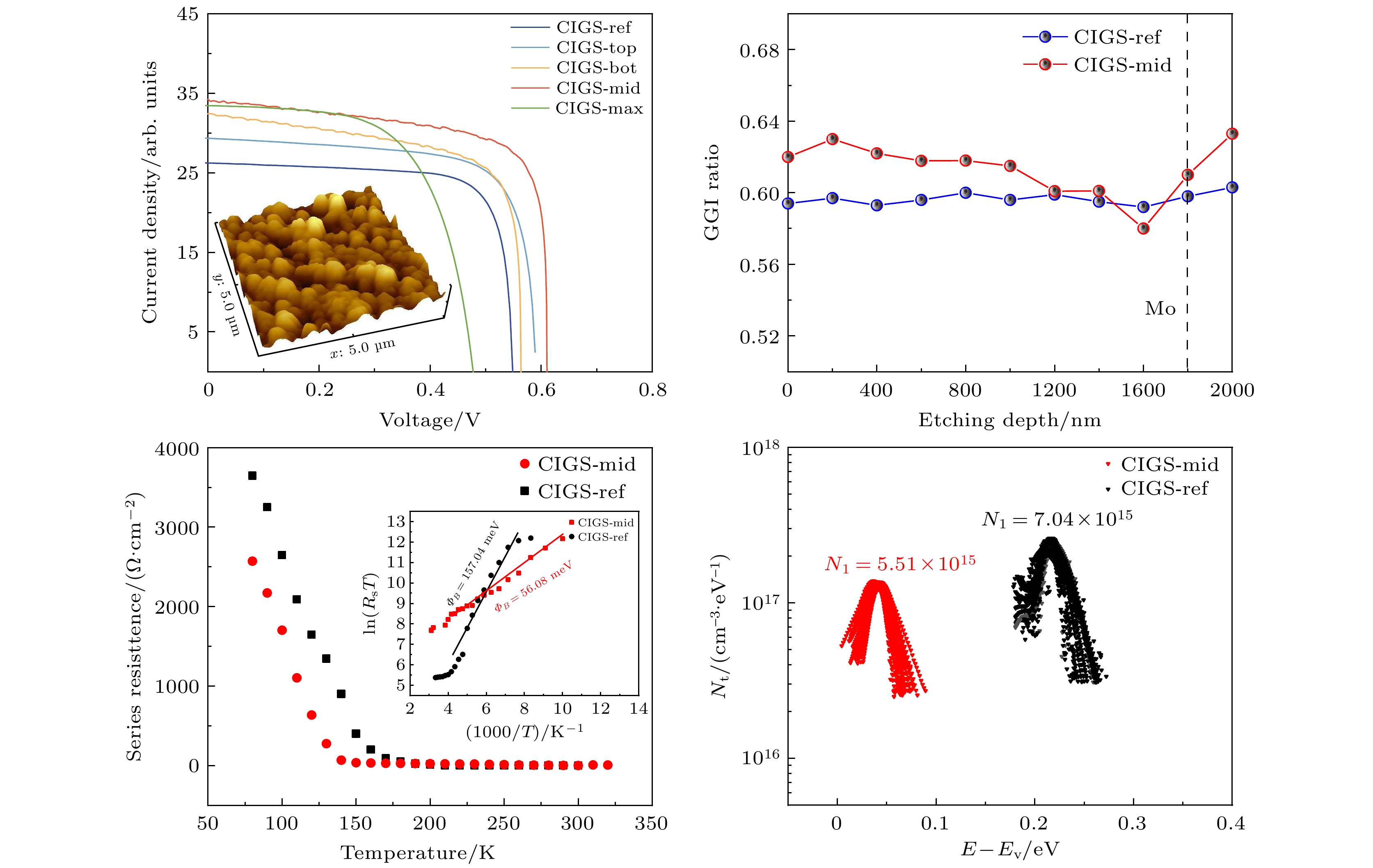
-
Keywords:
- Cu(In,Ga)Se2 solar cells /
- magnetron sputtering /
- V-band gap /
- defect characteristics
[1] Cheng K, Shen X F, Liu J L, Liu X S, Du Z L 2021 Sol. Energy 217 70
 Google Scholar
[2] Nakamura M, Yamaguchi K, Kimoto Y, Yasaki Y, Kato T, Sugimoto H 2019 IEEE J. Photovoltaics 9 1863
Google Scholar
[3] Gao Q Q, Yuan S J, Zhou Z J, Kou D X, Zhou W H, Meng Y N, Qi Y F, Han L T, Wu S X 2022 Small 18 2203443
Google Scholar
[4] Wang Y H, Tu L H, Chang Y L , Lin S K, Lin T Y, Lai C H 2021 ACS Appl. Energy Mater. 4 11555
Google Scholar
[5] Hsu C H, Ho W H, Wei S Y, Lai C H 2017 Adv. Energy Mater. 7 1602571
Google Scholar
[6] Hsu C H, Su Y S, Wei S Y, Chen C H, Ho W H, Chang C, Wu Y H, Lin C J, Lai C H 2015 Prog. Photovolt. 23 1621
Google Scholar
[7] Dai W L, Gao Z R, Li J J, Qin S M, Wang R B, Xu H Y, Wang X Z, Gao C, Teng X Y, Zhang Y, Hao X J, Wang Y L, Yu W 2021 ACS Appl. Mater. Interfaces 13 49414
Google Scholar
[8] Wang Y H, Ho P H, Huang W C, Tu L H, Chang H F, Cai C H, Lai C H 2020 ACS Appl. Mater. Interfaces 12 28320
Google Scholar
[9] Kong Y F, Li J M, Ma Z Y, Chi Z, Xiao X D 2020 J. Mater. Chem. A. 8 9760
Google Scholar
[10] Hoang V Q, Jeon D H, Park H K, Kim S Y, Kim W H, Hwang D K, Lee J, Son D H, Yang K J, Kang J K, Jo W 2023 ACS Appl. Energy Mater. 6 12180
Google Scholar
[11] Giraldo S, Fonoll-Rubio R, Jehl Li-Kao Z, et al. 2020 Prog. Photovolt. 29 334
Google Scholar
[12] Wan X J, Yuan M Y, Zeng C H, Lin R X, Li D Y, Hong R J 2024 Sol. Energy 273 112510
Google Scholar
[13] Sun Y L, Qin S M, Ding D L, Gao H F, Zhou Q, Guo X Y, Gao C, Liu H X, Zhang Y, Yu W 2023 Chem. Eng. J. 455 140596
Google Scholar
[14] Al-Hattab M, Moudou L, Khenfouch M, Bajjou O, Chrafih Y, Rahmani K 2021 Sol. Energy 227 13
Google Scholar
[15] Kim S T, Bhatt V, Kim Y C, Jeong H J, Yun J H, Jang J H 2022 J. Alloys Compd. 899 163301
Google Scholar
[16] Busacca A C, Rocca V, Curcio L, et al. 2014 International Conference on Renewable Energy Research and Application (ICRERA), IEEE Milwaukee, WI, USA, October 19–22, 2014 p964
[17] Ishizuka S, Yamada A, Fons P J, Shibata H, Niki S 2013 Appl. Phys. Lett. 103 143903
Google Scholar
[18] Carron R, Nishiwaki S, Feurer T, Hertwig R, Avancini E, Löckinger J, Yang S C, Buecheler S, Tiwari A N 2019 Adv. Energy Mater. 9 1900408
Google Scholar
[19] Zhao Y H, Yuan S J, Kou D X, Zhou Z J, Wang X S, Xiao H Q, Deng Y Q, Cui C C, Chang Q Q, Wu S X 2020 ACS Appl. Mater. 12 12717
Google Scholar
[20] Witte W, Abou-Ras D, Albe K, et al. 2015 Prog. Photovolt. 23 717
Google Scholar
[21] Venkatalaxmi A, Padmavathi B S, Amaranath T 2004 Fluid Dyn. Res. 35 229
Google Scholar
[22] Thompson C P, Chen L, Shafarman W N, Lee J, Fields S, Birkmire R W 2015 IEEE 42nd Photovoltaic Specialist Conference (PVSC) Orleans, LA, USA, June 14–19, 2015 p1
[23] Chantana J, Hironiwa D, Watanabe T, Teraji S, Kawamura K, Minemoto T 2015 Sol. Energy Mat. Sol. C. 133 223
Google Scholar
[24] Decock K, Khelifi S, Burgelman M 2011 Sol. Energy Mat. Sol. C. 95 1550
Google Scholar
-
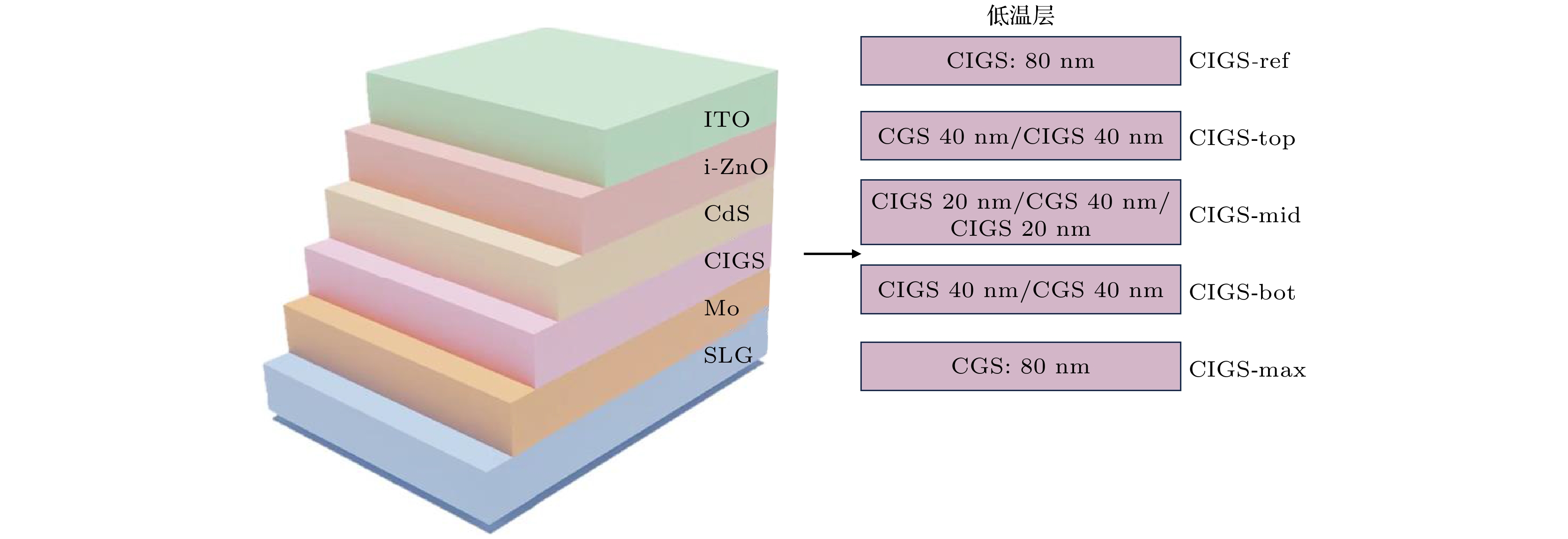
图 1 CIGS太阳电池结构示意图及低温层结构示意图
Fig. 1. Schematic diagram of CIGS solar cell structure and low-temperature layer structure.
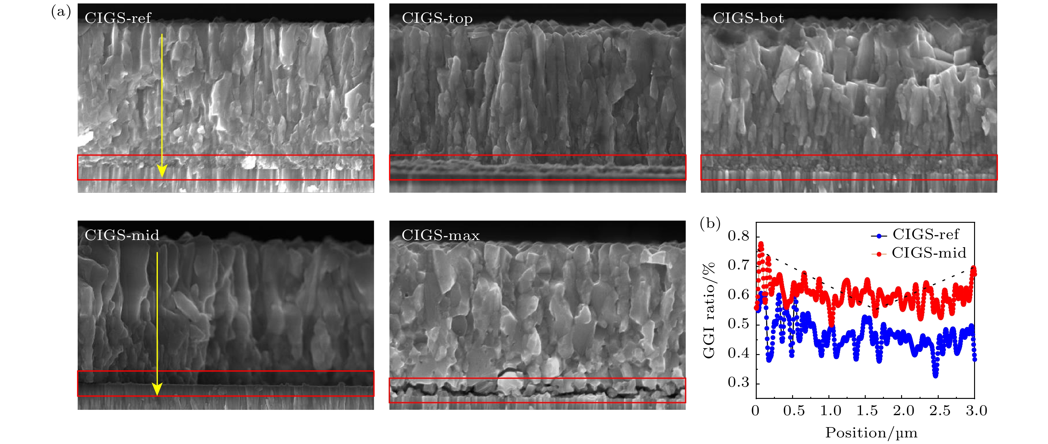
图 2 (a) 不同结构低温层所制备的CIGS薄膜的截面SEM图; (b) CIGS-ref和CIGS-mid的EDS线扫描图绘制的Ga梯度带隙图
Fig. 2. (a) Cross-sectional SEM images of CIGS films prepared for low-temperature layers with different structures; (b) Ga gradient bandgap plot plotted by EDS line scan plots of CIGS-ref and CIGS-mid.
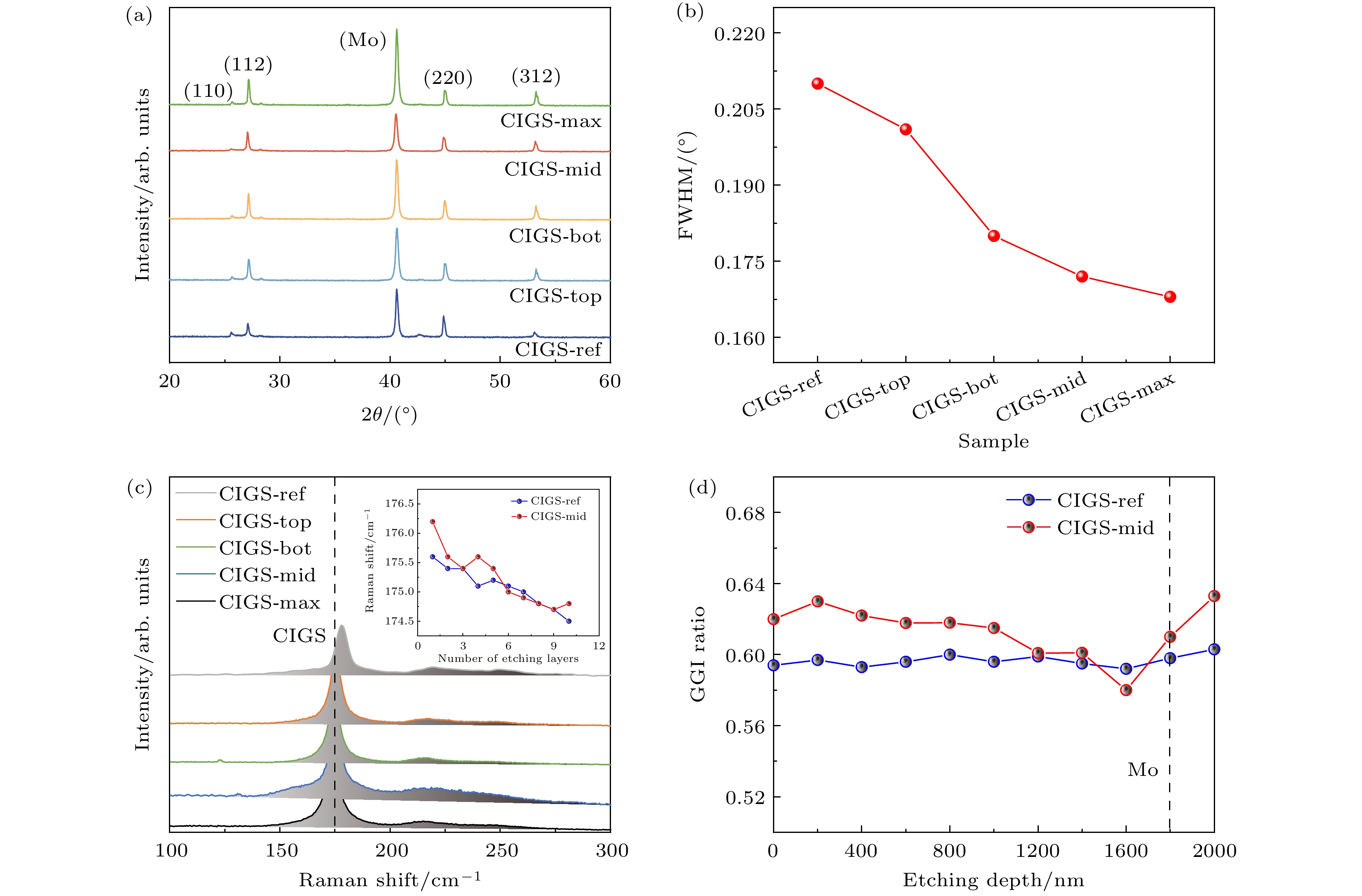
图 4 (a) CIGS吸收层在不同结构低温层条件下的XRD谱图; (b) (112) 峰的半峰宽图; (c) CIGS吸收层在不同结构低温层条件下的Raman结果及其吸收层深度上的CIGS峰位置; (d) 通过XPS得到CIGS-ref和CIGS-mid的GGI数据图
Fig. 4. (a) XRD of CIGS absorber layer under different structures of low temperature layers; (b) half-peak width plot of peak (112); (c) Raman results of CIGS absorber layers under different structural low-temperature layer conditions and CIGS peak positions on the depth of the absorber layer; (d) GGI data plots of CIGS-ref and CIGS-mid obtained by XPS.
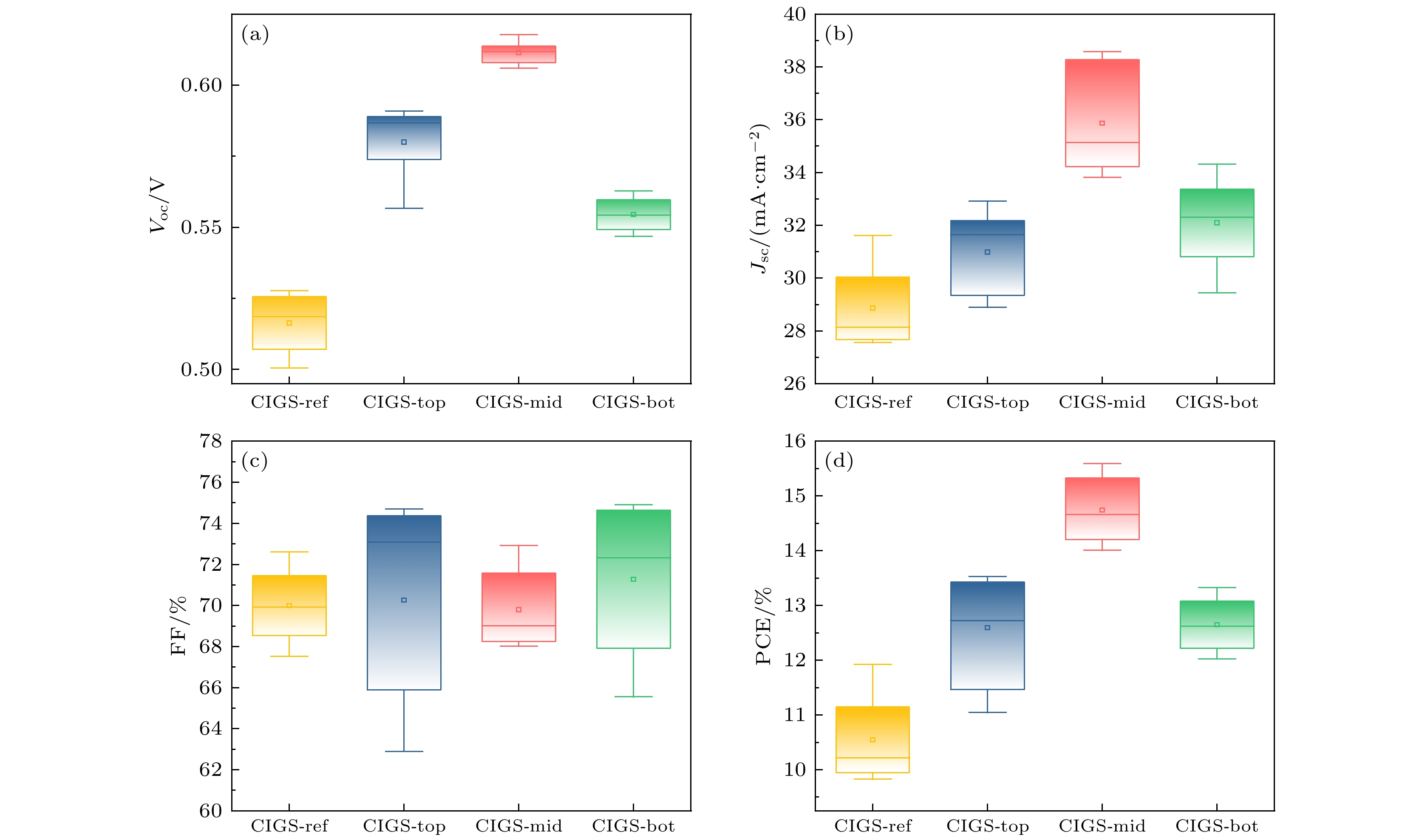
图 5 基于不同Ga梯度结构条件下制备的CIGS太阳电池的性能参数箱线图 (a) VOC; (b) JSC; (c) FF; (d) PCE
Fig. 5. Box plots of performance parameters of CIGS solar cells prepared under different Ga gradient structure conditions: (a) VOC; (b) JSC; (c) FF; (d) PCE.
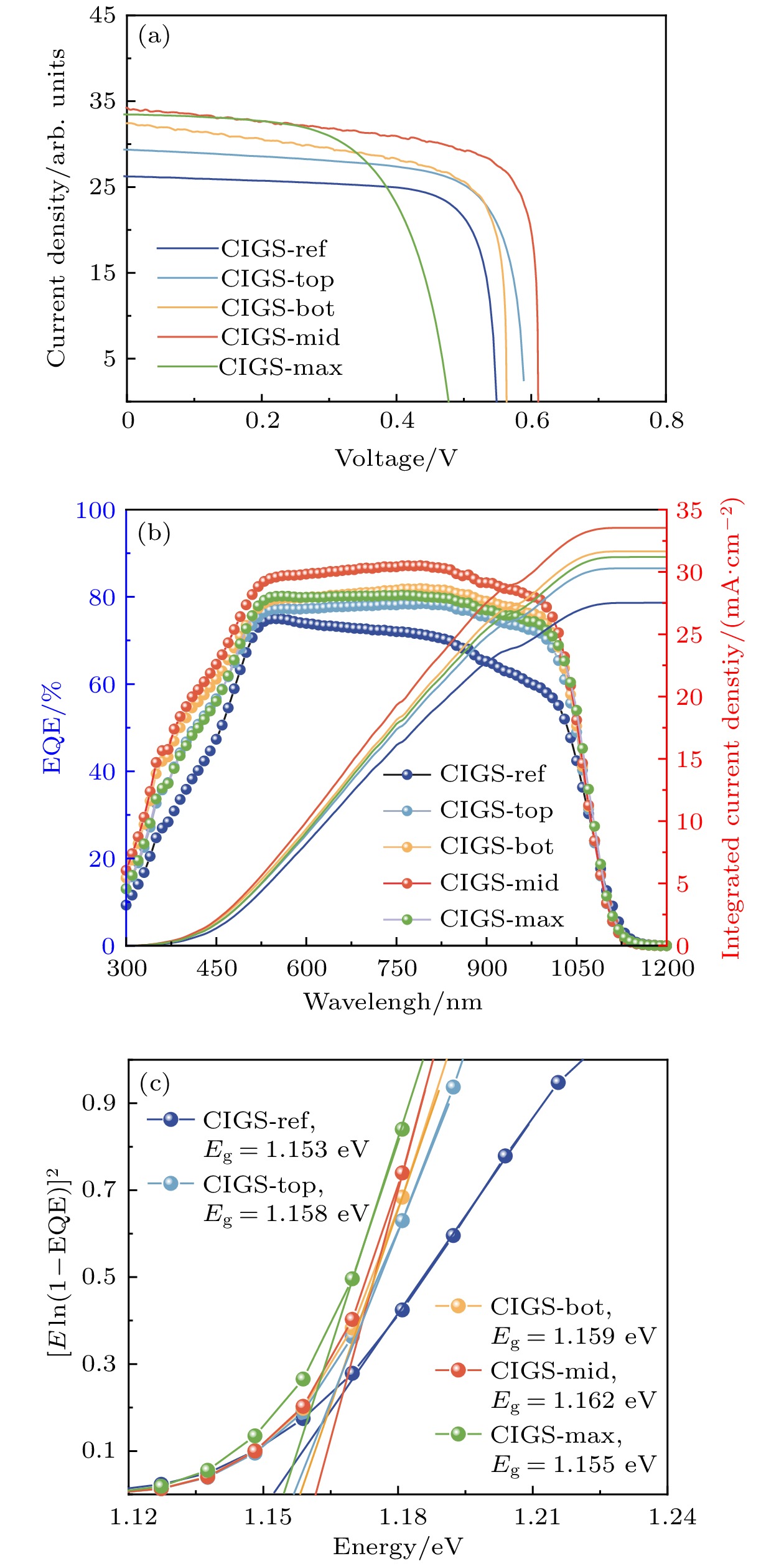
图 6 基于不同Ga梯度结构条件下制备的CIGS太阳电池的 (a) J-V曲线, (b) EQE曲线, 以及 (c) 其带隙图
Fig. 6. (a) J-V curves and (b) EQE curves of CIGS solar cells prepared under different Ga gradient structure conditions and (c) its bandgap diagram.
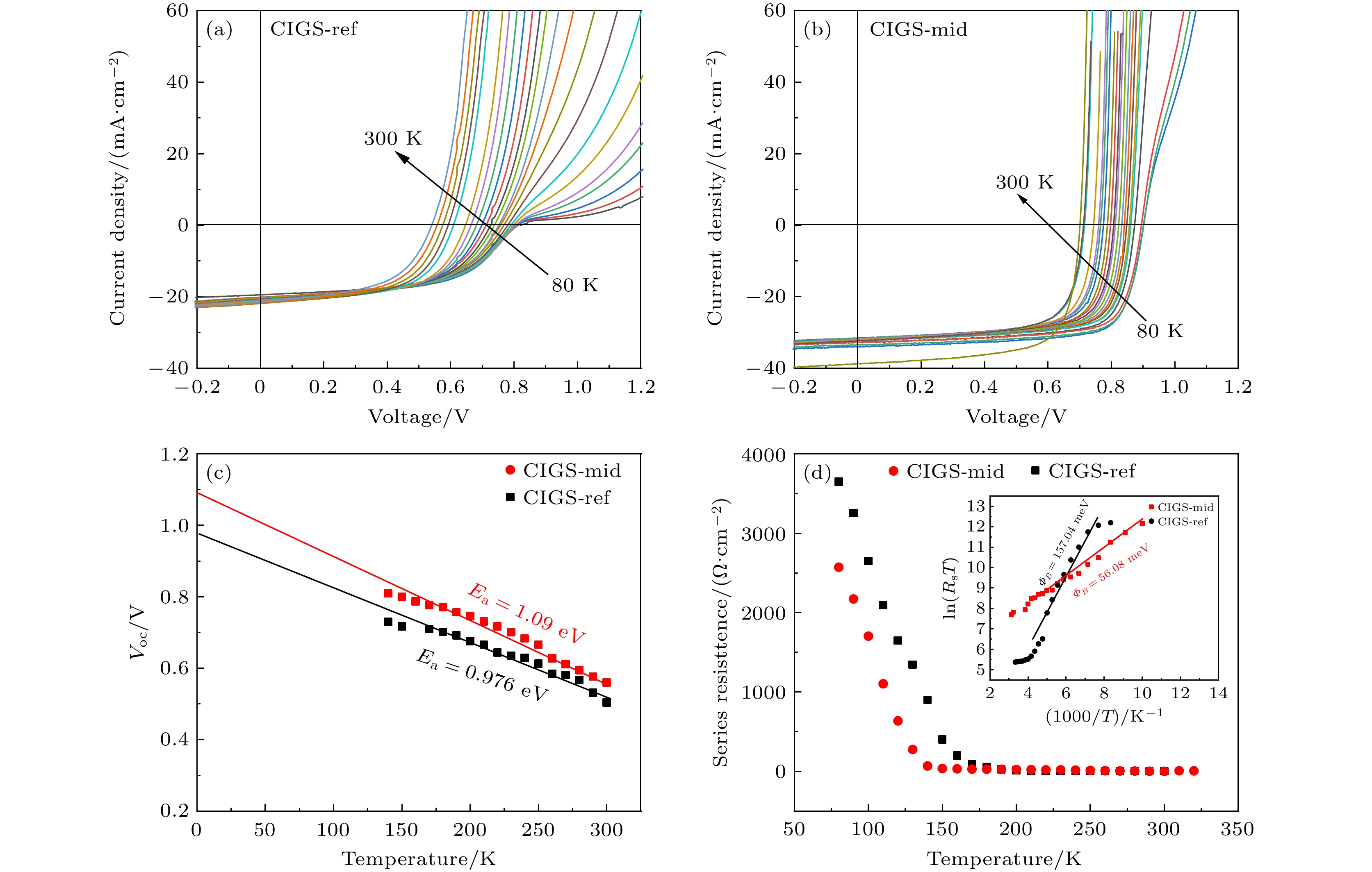
图 7 在80—300 K的温度范围内, (a) CIGS-ref和(b) CIGS-mid样品的电流密度-电压(J-V)特性; (c) 两个样品的VOC与T的关系曲线; (d) 暗J-V下Rs与T的关系曲线(插图为ln(RsT)与 1000/T 的关系曲线)
Fig. 7. (a), (b) Current density-voltage (J-V) characteristics of CIGS-ref and CIGS-mid samples over a temperature range of 80 to 300 K; (c) VOC/T curves of the two samples; (d) relationship between Rs and T under dark J-V (Insert is relationship curve between $ {\mathrm{l}}{\mathrm{n}}\;({R}_{{\mathrm{s}}}\cdot T) $ and 1000/T).
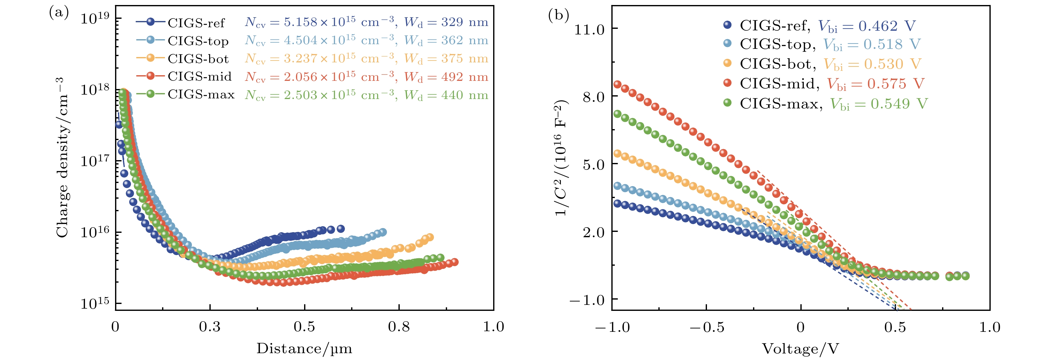
图 8 样品 CIGS-ref, CIGS-top, CIGS-bot, CIGS-mid, CIGS-max (a)载流子浓度NCV与耗尽区宽度Wd的分布图及(b) 1/C2与外置偏压V的关系图
Fig. 8. , The distribution plots of (a) carrier concentration NCV and the depletion zone width Wd and (b) the relationship between 1/C2 and external bias V of the CIGS-ref, CIGS-top, CIGS-bot, CIGS-mid, CIGS-max, respectively.
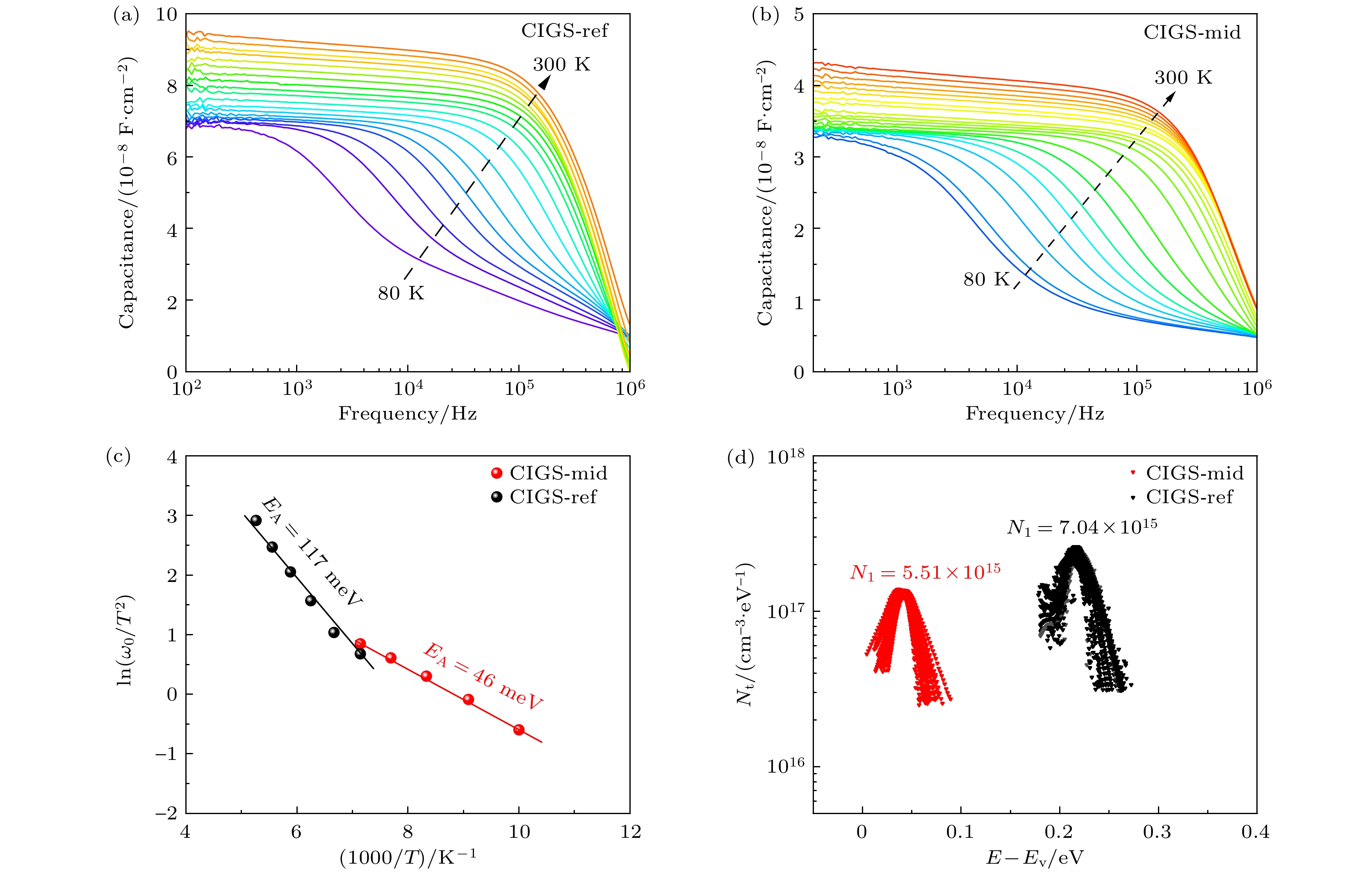
图 9 (a) 样品CIGS-ref导纳谱; (b) 样品CIGS-mid导纳谱; (c) 样品CIGS-ref和CIGS-mid为经计算提取的1000/T和$ {\mathrm{l}}{\mathrm{n}}({\omega }_{0}/{T}^{2}) $的关系图和相关缺陷激活能; (d) 样品CIGS-ref和薄膜CIGS-mid为所对应缺陷的态密度
Fig. 9. (a) CIGS-ref admittance spectrum of the sample; (b) CIGS-mid admittance spectra of the sample; (c) the CIGS-ref and CIGS-mid of the film are the calculated plots of 1000/T and $ {\mathrm{l}}{\mathrm{n}}({\omega }_{0}/{T}^{2}) $ and the associated defect activation energies; (d) the density of states of the defect corresponding to CIGS-ref and CIGS-mid.
表 1 国内外主要CIGS研究机构的研究进展
Table 1. Research progress of major CIGS research institutions at home and abroad.
衬底材料 效率/% 机构 方法 钠钙玻璃 19.40 中国科学院 共蒸发 钠钙玻璃 21.70 ZSW 共蒸发 不锈钢 17.70 EMPA 共蒸发 不锈钢 19.40 Miasolé 共溅射 钠钙玻璃 15.80 河北大学 单靶溅射无硒化 聚酰亚胺 20.80 EMPA 共蒸发 钠钙玻璃 22.92 汉能 共蒸发 钠钙玻璃 23.35 Solar Frontier 共蒸发 注: ZSW: 德国巴登符腾堡太阳能与氢能源研究中心;
EMPA: 瑞士联邦材料科学与技术实验室. 下载: 导出CSV
表 2 CIGS太阳电池详细结构表
Table 2. Detailed structure of CIGS solar cells.
CIGS结构 衬底 低温层 高温层 缓冲层 窗口层 CIGS-ref Mo/Mo CIGS CIGS CdS i-ZnO CIGS-top Mo/Mo CIGS/CGS CIGS CdS i-ZnO CIGS-mid Mo/Mo CIGS/CGS/CIGS CIGS CdS i-ZnO CIGS-bot Mo/Mo CGS/CIGS CIGS CdS i-ZnO CIGS-max Mo/Mo CGS CIGS CdS i-ZnO
下载: 导出CSV
表 3 基于不同Ga梯度结构条件下制备的的CIGS太阳电池性能参数表
Table 3. Performance parameters of CIGS solar cells prepared under different Ga gradient structure conditions.
样品 VOC/mV PCE/% FF/% JSC/(mA·cm–2) CIGS-ref 546 10.79 70.14 28.22 CIGS-top 580 13.39 72.80 31.71 CIGS-mid 614 15.04 70.21 34.81 CIGS-bot 556 12.92 72.12 32.22 CIGS-max 482 10.62 63.39 34.73
下载: 导出CSV
-
[1] Cheng K, Shen X F, Liu J L, Liu X S, Du Z L 2021 Sol. Energy 217 70
Google Scholar
[2] Nakamura M, Yamaguchi K, Kimoto Y, Yasaki Y, Kato T, Sugimoto H 2019 IEEE J. Photovoltaics 9 1863
Google Scholar
[3] Gao Q Q, Yuan S J, Zhou Z J, Kou D X, Zhou W H, Meng Y N, Qi Y F, Han L T, Wu S X 2022 Small 18 2203443
Google Scholar
[4] Wang Y H, Tu L H, Chang Y L , Lin S K, Lin T Y, Lai C H 2021 ACS Appl. Energy Mater. 4 11555
Google Scholar
[5] Hsu C H, Ho W H, Wei S Y, Lai C H 2017 Adv. Energy Mater. 7 1602571
Google Scholar
[6] Hsu C H, Su Y S, Wei S Y, Chen C H, Ho W H, Chang C, Wu Y H, Lin C J, Lai C H 2015 Prog. Photovolt. 23 1621
Google Scholar
[7] Dai W L, Gao Z R, Li J J, Qin S M, Wang R B, Xu H Y, Wang X Z, Gao C, Teng X Y, Zhang Y, Hao X J, Wang Y L, Yu W 2021 ACS Appl. Mater. Interfaces 13 49414
Google Scholar
[8] Wang Y H, Ho P H, Huang W C, Tu L H, Chang H F, Cai C H, Lai C H 2020 ACS Appl. Mater. Interfaces 12 28320
Google Scholar
[9] Kong Y F, Li J M, Ma Z Y, Chi Z, Xiao X D 2020 J. Mater. Chem. A. 8 9760
Google Scholar
[10] Hoang V Q, Jeon D H, Park H K, Kim S Y, Kim W H, Hwang D K, Lee J, Son D H, Yang K J, Kang J K, Jo W 2023 ACS Appl. Energy Mater. 6 12180
Google Scholar
[11] Giraldo S, Fonoll-Rubio R, Jehl Li-Kao Z, et al. 2020 Prog. Photovolt. 29 334
Google Scholar
[12] Wan X J, Yuan M Y, Zeng C H, Lin R X, Li D Y, Hong R J 2024 Sol. Energy 273 112510
Google Scholar
[13] Sun Y L, Qin S M, Ding D L, Gao H F, Zhou Q, Guo X Y, Gao C, Liu H X, Zhang Y, Yu W 2023 Chem. Eng. J. 455 140596
Google Scholar
[14] Al-Hattab M, Moudou L, Khenfouch M, Bajjou O, Chrafih Y, Rahmani K 2021 Sol. Energy 227 13
Google Scholar
[15] Kim S T, Bhatt V, Kim Y C, Jeong H J, Yun J H, Jang J H 2022 J. Alloys Compd. 899 163301
Google Scholar
[16] Busacca A C, Rocca V, Curcio L, et al. 2014 International Conference on Renewable Energy Research and Application (ICRERA), IEEE Milwaukee, WI, USA, October 19–22, 2014 p964
[17] Ishizuka S, Yamada A, Fons P J, Shibata H, Niki S 2013 Appl. Phys. Lett. 103 143903
Google Scholar
[18] Carron R, Nishiwaki S, Feurer T, Hertwig R, Avancini E, Löckinger J, Yang S C, Buecheler S, Tiwari A N 2019 Adv. Energy Mater. 9 1900408
Google Scholar
[19] Zhao Y H, Yuan S J, Kou D X, Zhou Z J, Wang X S, Xiao H Q, Deng Y Q, Cui C C, Chang Q Q, Wu S X 2020 ACS Appl. Mater. 12 12717
Google Scholar
[20] Witte W, Abou-Ras D, Albe K, et al. 2015 Prog. Photovolt. 23 717
Google Scholar
[21] Venkatalaxmi A, Padmavathi B S, Amaranath T 2004 Fluid Dyn. Res. 35 229
Google Scholar
[22] Thompson C P, Chen L, Shafarman W N, Lee J, Fields S, Birkmire R W 2015 IEEE 42nd Photovoltaic Specialist Conference (PVSC) Orleans, LA, USA, June 14–19, 2015 p1
[23] Chantana J, Hironiwa D, Watanabe T, Teraji S, Kawamura K, Minemoto T 2015 Sol. Energy Mat. Sol. C. 133 223
Google Scholar
[24] Decock K, Khelifi S, Burgelman M 2011 Sol. Energy Mat. Sol. C. 95 1550
Google Scholar

 下载:
下载:
计量
- 文章访问数: 3195
- PDF下载量: 70
- 被引次数: 0
