-
晶界结构在石墨烯变形过程中的演变规律及作用机制对理解石墨烯变形行为具有重要意义. 本文采用三模晶体相场模型, 在原子尺度上深入研究了石墨烯小角对称倾侧晶界处位错在应变作用下的演化机理. 结果发现, 随着晶界角的增大, 晶界位错密度降低, 特定类型的位错(5|8|7位错和5|7位错)数量上升. 在与晶界平行的应力加载下, 晶界处位错因C—C键断裂或旋转, 转化为5|7或5|9型位错, 这是由于较大自由能的位错在拉伸下演化为小能量的位错, 这有利于石墨烯性能的提高. 拉伸载荷下, 含不同角度晶界的体系自由能变化呈现相同趋势: 初始下降至拐点后出现异常上升, 位错行为不能有效缓解体系因持续加载造成的应力集中, 导致失效. 本工作有助于从原子尺度理解石墨烯微观力学行为.
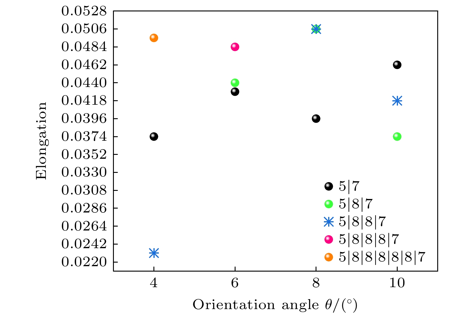
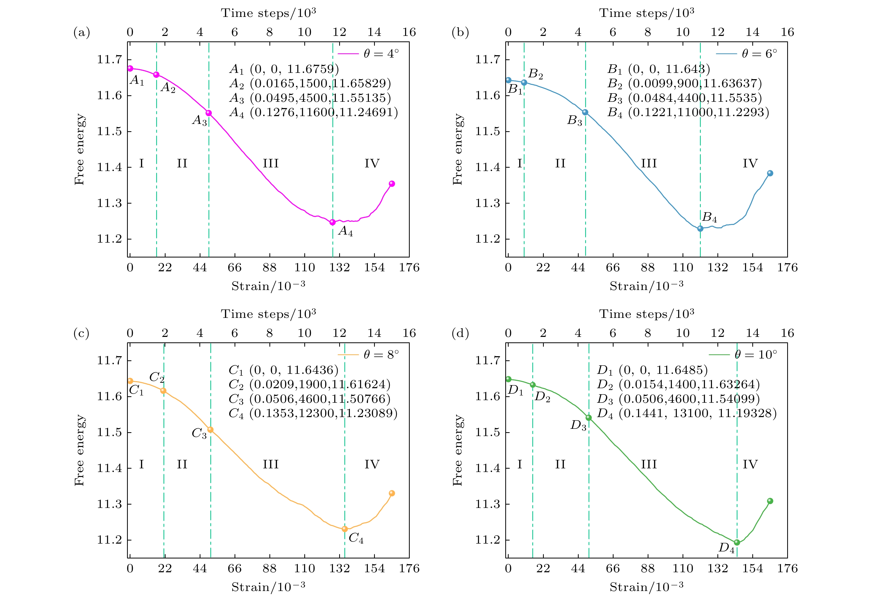
The evolution law and mechanism of grain boundary structure in the deformation process of graphene are of great significance for understanding the deformation behavior of graphene and optimizing its mechanical properties. In this work, single-layer graphene is taken as the research object and a double crystalline graphene model is established by using the three-mode phase-field crystal method, thereby in depth ascertaining the evolution mechanism of dislocations at small-angle symmetrical tilt grain boundaries in graphene under strain. In view of the relaxation and deformation process, the relationship between the number of multiple dislocations and the grain boundary angle of graphene is studied on an atomic scale, and the deformation and failure mechanism of double crystalline graphene under tensile load are revealed, and also discussed from the perspective of the free energy. It is found that, after relaxation, with the increase of grain boundary angle, the density of dislocations at the grain boundary decreases, and the number of specific types of dislocations (5|8|7 and 5|7 dislocations) increases. Under stress loading parallel to the grain boundary, the changes of free energy of the systems containing grain boundaries with different angles show the same trend: at first, they fall to the inflection point and then rise abnormally, and the dislocation behavior cannot effectively alleviate the stress concentration caused by continuous loading in the system, leading to failure finally. Under tensile load, the free energy changes of the systems are divided into four stages, they being stage (I), in which the dislocations at grain boundaries are slightly deformed but do not change their structure, stage (II), in which dislocations at the grain boundaries are transformed into 5|7 or 5|9 dislocation due to C—C bond fracture or rotation, and the dislocations that are “incompatible” have higher energy, making them more conducive to improving the tensile properties of graphene, stage (III), in which the 5|7 and 5|9 dislocations begin to fail, and the free energy shows a tendency to decrease significantly, and stage (IV), in which the double crystalline graphene systems are completely in failure. The system with a grain boundary angle of 10° exhibits the most substantial deduction in free energy in stages (I), (II), and (III), and possesses the highest overall tensile strength. This work contributes to understanding the micromechanical behavior of graphene on an atomic scale. -
Keywords:
- phase-field crystal method /
- graphene /
- grain-boundaries /
- dislocations
[1] 林彰乾, 郑伟, 李浩, 王东君 2021 金属学报 57 111
 Google Scholar
Lin Z Q, Zhen W, Li H, Wang D J 2021 Acta. Metall. Sin. 57 111
 Google Scholar
[2] Lee C, Wei X, Kysar J W, Hone J 2008 Science 321 385
 Google Scholar
[3] Cao K, Feng S Z, Han Y, Gao L B, Hue Ly T, Xu Z P, Lu Y 2020 Nat. Commun. 11 284
 Google Scholar
[4] Liu J, Hei L F, Song J H, Li C M, Tang W Z, Chen G C, Lu F X 2014 Diam. Relat. Mater. 46 42
 Google Scholar
[5] Huang P Y, Ruiz-Vargas C S, van der Zande A M, et al. 2011 Nature 469 389
 Google Scholar
[6] Hashimoto A, Suenaga K, Gloter A, Urita K, Iijima S 2004 Nature 430 870
 Google Scholar
[7] Meyer J C, Kisielowski C, Erni R, Rossell M D, Crommie M F, Zettl A 2008 Nano Lett. 8 3582
 Google Scholar
[8] He L C, Guo S S, Lei J C, Sha Z D, Liu Z H 2014 Carbon 75 124
 Google Scholar
[9] 周文权 2019 博士学位论文(西安: 西北工业大学)
Zhou W Q 2019 Ph. D. Dissertation (Xi’an: Northwestern Polytechnical University
[10] Shekhawat A, Ritchie R O 2016 Nat. Commun. 7 10546
 Google Scholar
[11] Zhang J F, Zhao J J, Lu J P 2012 ACS Nano 6 2704
 Google Scholar
[12] Heo J, Han J 2023 Nanotechnology 34 415704
 Google Scholar
[13] Grantab R, Shenoy V B, Ruoff R S 2010 Science 330 946
 Google Scholar
[14] Wei Y J, Wu J T, Yin H Q, Shi X H, Yang R G, Dresselhaus M 2012 Nat. Mater. 11 759
 Google Scholar
[15] Lehtinen O, Kurasch S, Krasheninnikov A V, Kaiser U 2013 Nat. Commun. 4 2098
 Google Scholar
[16] Liu Z, Suenaga K, Harris P J F, Iijima S 2009 Phys. Rev. Lett. 102 015501
 Google Scholar
[17] Zhao Y H, Tian X L, Zhao B J, et al. 2018 Sci. Adv. Mater. 10 1793
 Google Scholar
[18] Zhang J B, Wang H F, Kuang W W, Zhang Y C, Li S, Zhao Y H, Herlach D M 2018 Acta Mater. 148 86
 Google Scholar
[19] Guo Q W, Hou H, Wang K L, Li M X, Liaw P K, Zhao Y H 2023 npj Comput. Mater. 9 185
 Google Scholar
[20] Xin T Z, Zhao Y H, Mahjoub R, Jiang J X, Ferry M 2021 Sci. Adv. 7 eabf3039
 Google Scholar
[21] Xin T Z, Tang S, Ji F, Cui L Q, He B B, Lin X, Tian X L, Hou H, Zhao Y H, Ferry M 2022 Acta Mater. 239 118248
 Google Scholar
[22] Zhao Y H, Zhang B, Hou H, Chen W P, Wang M 2019 J. Mater. Sci. Technol. 35 1044
 Google Scholar
[23] Chen L Q, Zhao Y H 2022 Prog. Mater. Sci. 124 100868
 Google Scholar
[24] Zhao Y H, Xin T Z, Tang S, Wang H F, Fang X D, Hou H 2024 MRS Bull. 49 613
 Google Scholar
[25] Zhao Y H, Xing H, Zhang L J, et al. 2023 Acta Metall. Sin. (Engl. Lett. ) 36 1749
 Google Scholar
[26] Zhao Y H 2024 npj Comput. Mater. 2 e44
 Google Scholar
[27] Zhao Y H 2023 npj Comput. Mater. 9 94
 Google Scholar
[28] Kuang W W, Wang H F, Li X, Zhang J B, Zhou Q, Zhao Y H 2018 Acta Mater. 159 16
 Google Scholar
[29] Song Z, Li H Q, Wang X N, Tian X L, Hou H, Zhao Y H 2023 J. Mater. Res. Technol. 27 6501
 Google Scholar
[30] Zhong L, Gao H J, Li X Y 2020 Extreme Mech. Lett. 37 100699
 Google Scholar
[31] Meca E, Lowengrub J, Kim H, Mattevi C, Shenoy V B 2013 Nano Lett. 13 5692
 Google Scholar
[32] Li H Q, Wang X N, Zhang H B, Tian X L, Hou H, Zhao Y H 2022 Front. Mater. 9 875519
 Google Scholar
[33] Elder K R, Katakowski M, Haataja M, Grant M 2002 Phys. Rev. Lett. 88 245701
 Google Scholar
[34] Tian X L, Zhao Y H, Gu T, Guo Y L, Xu F Q, Hou H 2022 Mater. Sci. Eng. 849 143485
 Google Scholar
[35] Zhao Y H, Liu K X, Zhang H B, Tian X L, Jiang Q L, Murugadoss V, Hou H 2022 Adv. Compos. Hybrid Mater. 5 2546
 Google Scholar
[36] Kim K, Lee Z, Regan W, Kisielowski C, Crommie M F, Zettl A 2011 ACS Nano 5 2142
 Google Scholar
[37] Akhukov M A, Fasolino A, Gornostyrev Y N, Katsnelson M I 2012 Phys. Rev. B 85 115407
 Google Scholar
[38] Hirvonen P, Ervasti M M, Fan Z, et al. 2016 Phys. Rev. B 94 035414
 Google Scholar
[39] Guo H J, Zhao Y H, Sun Y Y, Tian J Z, Hou H, Qi K W, Tian X L 2019 Micro Nanostruct. 129 163
 Google Scholar
[40] Elder K R, Grant M 2004 Phys. Rev. E 70 051605
 Google Scholar
-
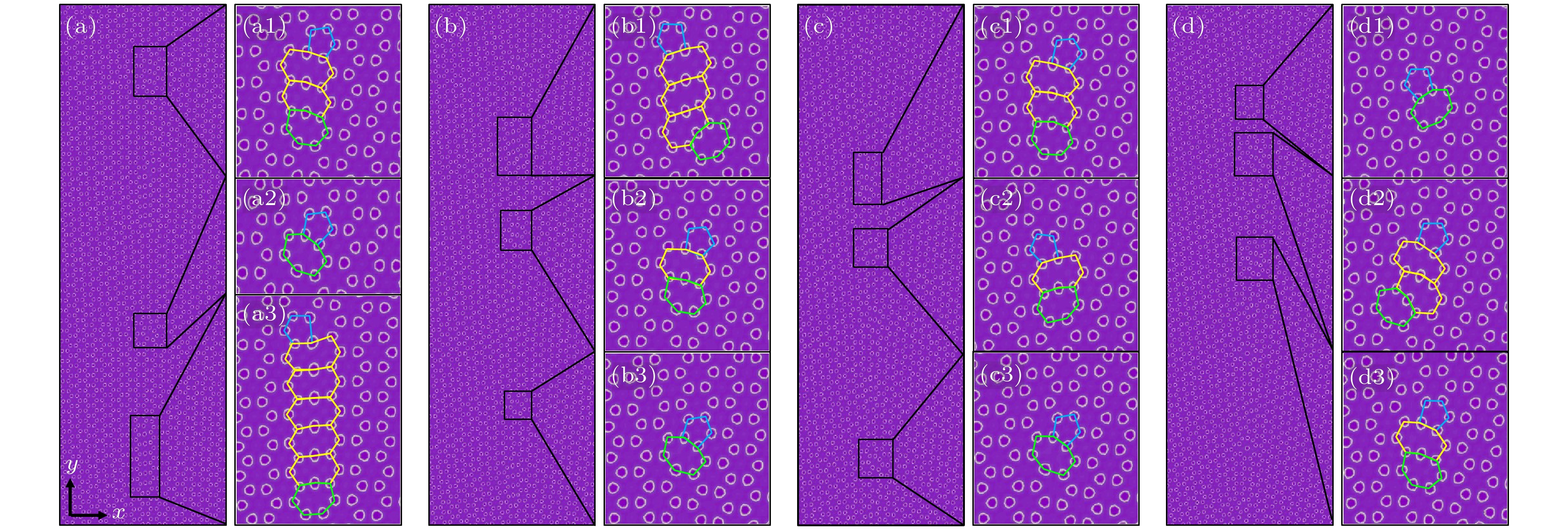
图 2 石墨烯气相结晶图(蓝、绿、黄色标记石墨烯的五角元胞、七角元胞、八角元胞) (a)—(d)晶界角分别为4°, 6°, 8°, 10°, 其中黑框中为晶界处位错; (a1)—(a3), (b1)—(b3), (c1)—(c3), (d1)—(d3)是对应的放大图
Fig. 2. Vapor crystallization diagram of graphene: (a)–(d) Grain boundary angles are 4°, 6°, 8° and 10°, respectively, dislocations at grain boundaries are shown in the black box; (a1)–(a3), (b1)–(b3), (c1)–(c3), (d1)–(d3) are the corresponding enlarged images. Blue, green, yellow labeled graphene pentagonal cells, heptagonal cells, octagonal cells
图 3 双晶石墨烯体系中晶界处位错数目统计结果 (a) 晶界角为4°—10°的总位错数目; (b) 晶界角为4°—10°的各种位错数目
Fig. 3. Statistical results of the number of dislocations at the grain boundaries in the double crystalline graphene system: (a) Total number of dislocations at grain boundary angles of 4°–10°; (b) number of various dislocations at grain boundary angles of 4°–10°.
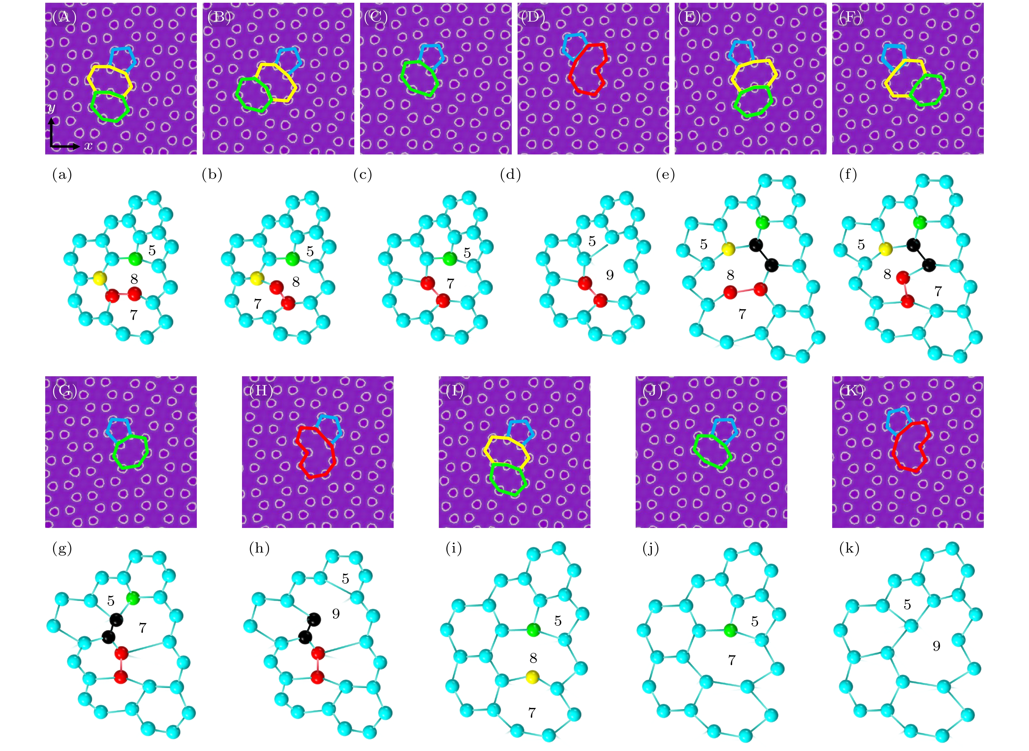
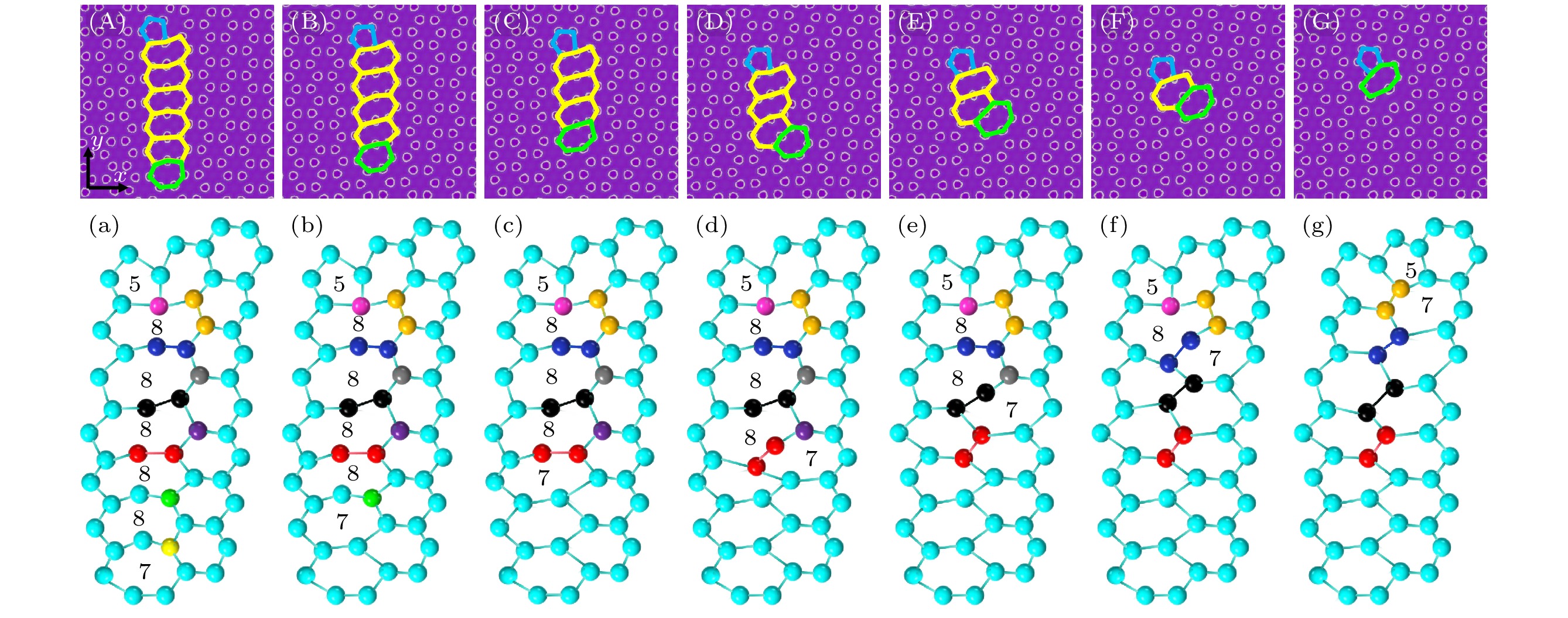
图 4 石墨烯晶界5|7位错在应变下的演化图 (A)—(C), (D)—(G), (H)—(I), (J)—(L)分别对应晶界角为4°, 6°, 8°, 10°的石墨烯晶界5|7位错在应变下的演化图; (a)—(c), (d)—(g), (h)—(i), (j)—(l)为对应的演化过程示意图; (A)—(C)的应变$\varepsilon $分别为0, 0.0297, 0.0352; (D)—(G) 的应变$\varepsilon $分别为0, 0.0286, 0.0308, 0.0352; (H), (I) 的应变$\varepsilon $分别为0, 0.0363; (J)—(L) 的应变$\varepsilon $分别为0, 0.0297, 0.0363 (演化过程示意图中标记的5, 7, 8, 9分别代表石墨烯五、七、八、九角元胞, 分别对应相应演化图中石墨烯蓝、绿、黄、红色标记的五、七、八、九角元胞, 图5—8中标记解释与此相同)
Fig. 4. Evolution diagram of 5|7 dislocations at graphene grain boundaries under strain: (A)–(C), (D)–(G), (H)–(I), (J)–(L) are the evolution diagrams of 5|7 dislocations at graphene grain boundaries under strain for corresponding grain boundary angles of 4°, 6°, 8° and 10°; (a)–(c), (d)–(g), (h)–(i), (j)–(l) are the evolution process diagrams. The strains $\varepsilon $ of (A)–(C) are 0, 0.0297, 0.0352, (D)–(G) are 0, 0.0286, 0.0308, 0.0352, (H), (I) are 0, 0.0363, and (J)–(L) are 0, 0.0297, 0.0363. The 5, 7, 8, 9 marked in the evolution diagram represent the graphene pentagonal, heptagonal, octagonal, and nougonal cells respectively, corresponding to the pentagonal, heptagonal, octagonal, and nougonal cells marked in the corresponding evolution process diagram in blue, green, yellow, and red respectively. The explanations of labels in Figure 5-8 are the same as those in Figure 4.
图 5 石墨烯晶界5|8|7位错在应变下的演化图 (A)—(D), (E)—(H), (I)—(K)分别对应晶界角为6°, 8°, 10°的石墨烯晶界5|8|7位错在应变下的演化图; (a)—(d), (e)—(h), (i)—(k)是对应的演化过程示意图; (A)—(D)的应变$\varepsilon $分别为0, 0.0209, 0.0352, 0.0407, (E)—(H) 的应变$\varepsilon $分别为0, 0.0209, 0.0429, 0.0473, (I)—(K) 的应变$\varepsilon $分别为0, 0.0165, 0.0319
Fig. 5. Evolution diagram of 5|8|7 dislocations at graphene grain boundaries under strain: (A)–(D), (E)–(H), (I)–(K) are the evolution diagrams of 5|8|7 dislocations at graphene grain boundaries under strain for corresponding grain boundary angles of 6°, 8° and 10°; (a)–(d), (e)–(h), (i)–(k) are the corresponding evolution process diagrams; the strains $\varepsilon $ of (A)–(D) are 0, 0.0209, 0.0352, 0.0407, (E)–(H) are 0, 0.0209, 0.0429, 0.0473, (I)–(K) are 0, 0.0165, 0.0319.
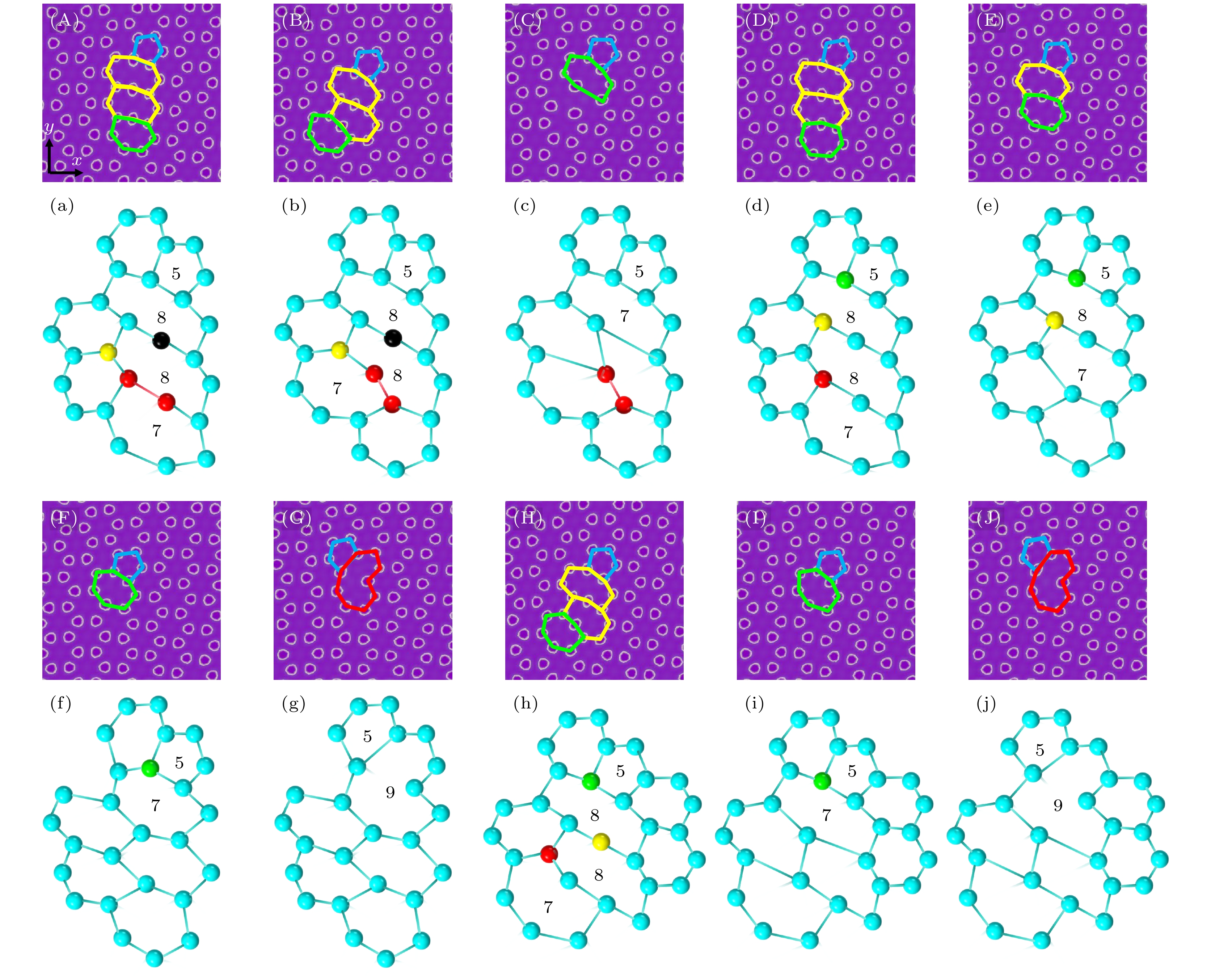
图 6 石墨烯晶界5|8|8|7位错在应变下的演化图 (A)—(C), (D)—(G), (H)—(J)分别对应晶界角为4°, 8°, 10°的石墨烯晶界5|8|8|7位错在应变下的演化图; (a)—(c), (d)—(g), (h)—(j)是对应的演化过程示意图; (A)—(C)的应变$\varepsilon $分别为0, 0.0165, 0.022, (D)—(G)的应变$\varepsilon $分别为0, 0.0253, 0.0363, 0.0473, (H)—(J)的应变$\varepsilon $分别为0, 0.0154, 0.0242
Fig. 6. Evolution diagram of 5|8|8|7 dislocations at graphene grain boundaries under strain: (A)–(C), (D)–(G), (H)–(J) are the evolution diagrams of 5|8|8|7 dislocations at graphene grain boundaries under strain for corresponding grain boundary angles of 4°, 8° and 10°; (a)–(c), (d)–(g), (h)–(j) are the corresponding evolution process diagrams; the strains $\varepsilon $ of (A)–(C) are 0, 0.0165, 0.022, (D)–(G) are 0, 0.0253, 0.0363, 0.0473, (H)–(J) are 0, 0.0154, 0.0242.
图 7 石墨烯晶界5|8|8|8|7位错在应变下的3种演化图 (A)—(C), (D)—(G), (H)—(M) 是晶界角为6°的石墨烯晶界5|8|8|8|7位错在应变下的3种演化图; (a)—(c), (d)—(g), (h)—(m)是对应的演化过程示意图; (A)—(C) 的应变$\varepsilon $分别为0, 0.0132, 0.0209, (D)—(G)的应变$\varepsilon $分别为0, 0.0132, 0.0242, 0.0297, (H)—(M)的应变$\varepsilon $分别为0, 0.099, 0.0187, 0.0264, 0.0407, 0.0462
Fig. 7. Three evolution diagrams of 5|8|8|8|7 dislocations at graphene grain boundaries under strain: (A)–(C), (D)–(G), (H)–(M) are three evolution diagrams of 5|8|8|8|7 dislocations at graphene grain boundaries under strain for the grain boundary angle of 6°; (a)–(c), (d)–(g), (h)–(m) are the corresponding evolution process diagrams; the strains $\varepsilon $ of (A)–(C) are 0, 0.0132, 0.0209, (D)–(G) are 0, 0.0132, 0.0242, 0.0297, (H)–(M) are 0, 0.099, 0.0187, 0.0264, 0.0407, 0.0462.
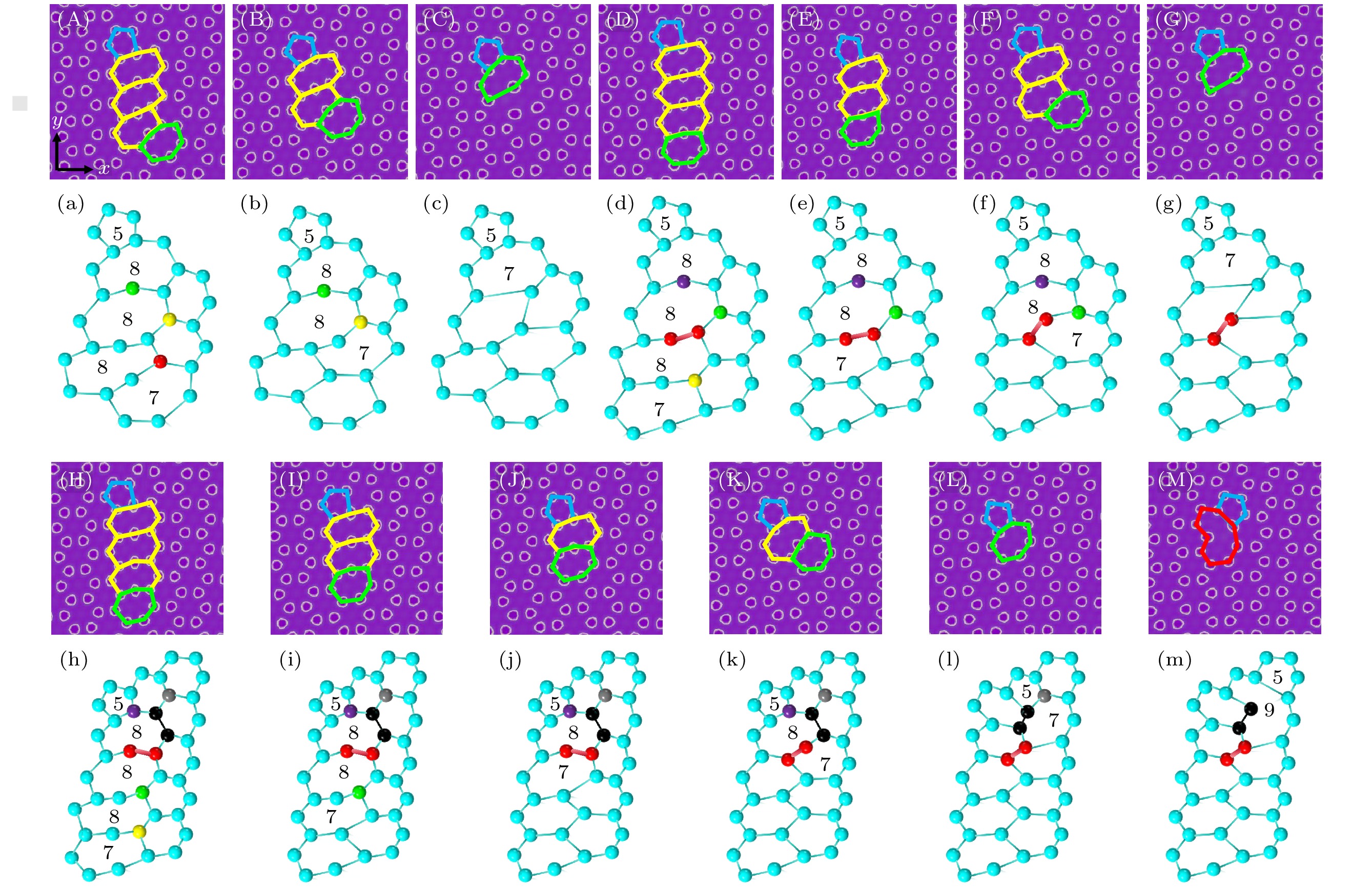
图 8 石墨烯晶界5|8|8|8|8|8|7位错在应变下的演化图 (A)—(G)晶界角为4°的石墨烯晶界5|8|8|8|8|8|7位错在应变下的演化图; (a)—(g)是演化过程示意图; (A)—(G)的应变$\varepsilon $分别为0, 0.0231, 0.0281, 0.0319, 0.0341, 0.0374, 0.0473
Fig. 8. Evolution diagram of 5|8|8|8|8|8|7 dislocations at graphene grain boundaries under strain: (A)–(G) are the evolution diagrams of 5|8|8|8|8|8|7 dislocations at graphene grain boundaries under strain for grain boundary angles of 4°; (a)–(g) are the evolution process diagrams; the strains $\varepsilon $ of (A)–(G) are 0, 0.0231, 0.0281, 0.0319, 0.0341, 0.0374, 0.0473.
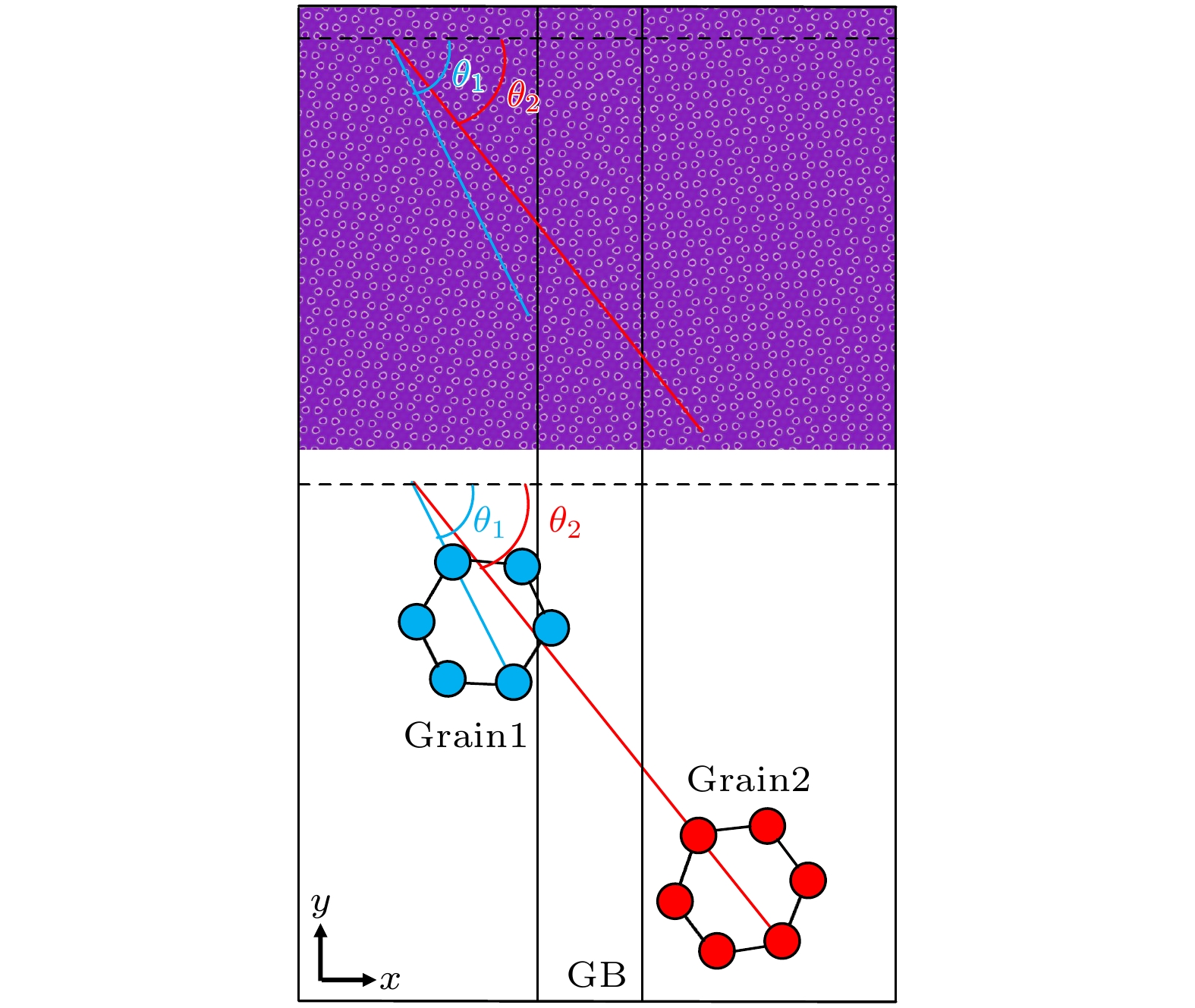
表 1 施加应力应变的参数
Table 1. Parameters for applying stress and strain.
试样 拉伸应
变方向晶粒取向角 晶界角
$\theta $/(°)${\theta _1}$/(°) ${\theta _2}$/(°) A $y$ 2 –2 4 B $y$ 3 –3 6 C $y$ 4 –4 8 D $y$ 5 –5 10 -
[1] 林彰乾, 郑伟, 李浩, 王东君 2021 金属学报 57 111
 Google Scholar
Lin Z Q, Zhen W, Li H, Wang D J 2021 Acta. Metall. Sin. 57 111
 Google Scholar
[2] Lee C, Wei X, Kysar J W, Hone J 2008 Science 321 385
 Google Scholar
[3] Cao K, Feng S Z, Han Y, Gao L B, Hue Ly T, Xu Z P, Lu Y 2020 Nat. Commun. 11 284
 Google Scholar
[4] Liu J, Hei L F, Song J H, Li C M, Tang W Z, Chen G C, Lu F X 2014 Diam. Relat. Mater. 46 42
 Google Scholar
[5] Huang P Y, Ruiz-Vargas C S, van der Zande A M, et al. 2011 Nature 469 389
 Google Scholar
[6] Hashimoto A, Suenaga K, Gloter A, Urita K, Iijima S 2004 Nature 430 870
 Google Scholar
[7] Meyer J C, Kisielowski C, Erni R, Rossell M D, Crommie M F, Zettl A 2008 Nano Lett. 8 3582
 Google Scholar
[8] He L C, Guo S S, Lei J C, Sha Z D, Liu Z H 2014 Carbon 75 124
 Google Scholar
[9] 周文权 2019 博士学位论文(西安: 西北工业大学)
Zhou W Q 2019 Ph. D. Dissertation (Xi’an: Northwestern Polytechnical University
[10] Shekhawat A, Ritchie R O 2016 Nat. Commun. 7 10546
 Google Scholar
[11] Zhang J F, Zhao J J, Lu J P 2012 ACS Nano 6 2704
 Google Scholar
[12] Heo J, Han J 2023 Nanotechnology 34 415704
 Google Scholar
[13] Grantab R, Shenoy V B, Ruoff R S 2010 Science 330 946
 Google Scholar
[14] Wei Y J, Wu J T, Yin H Q, Shi X H, Yang R G, Dresselhaus M 2012 Nat. Mater. 11 759
 Google Scholar
[15] Lehtinen O, Kurasch S, Krasheninnikov A V, Kaiser U 2013 Nat. Commun. 4 2098
 Google Scholar
[16] Liu Z, Suenaga K, Harris P J F, Iijima S 2009 Phys. Rev. Lett. 102 015501
 Google Scholar
[17] Zhao Y H, Tian X L, Zhao B J, et al. 2018 Sci. Adv. Mater. 10 1793
 Google Scholar
[18] Zhang J B, Wang H F, Kuang W W, Zhang Y C, Li S, Zhao Y H, Herlach D M 2018 Acta Mater. 148 86
 Google Scholar
[19] Guo Q W, Hou H, Wang K L, Li M X, Liaw P K, Zhao Y H 2023 npj Comput. Mater. 9 185
 Google Scholar
[20] Xin T Z, Zhao Y H, Mahjoub R, Jiang J X, Ferry M 2021 Sci. Adv. 7 eabf3039
 Google Scholar
[21] Xin T Z, Tang S, Ji F, Cui L Q, He B B, Lin X, Tian X L, Hou H, Zhao Y H, Ferry M 2022 Acta Mater. 239 118248
 Google Scholar
[22] Zhao Y H, Zhang B, Hou H, Chen W P, Wang M 2019 J. Mater. Sci. Technol. 35 1044
 Google Scholar
[23] Chen L Q, Zhao Y H 2022 Prog. Mater. Sci. 124 100868
 Google Scholar
[24] Zhao Y H, Xin T Z, Tang S, Wang H F, Fang X D, Hou H 2024 MRS Bull. 49 613
 Google Scholar
[25] Zhao Y H, Xing H, Zhang L J, et al. 2023 Acta Metall. Sin. (Engl. Lett. ) 36 1749
 Google Scholar
[26] Zhao Y H 2024 npj Comput. Mater. 2 e44
 Google Scholar
[27] Zhao Y H 2023 npj Comput. Mater. 9 94
 Google Scholar
[28] Kuang W W, Wang H F, Li X, Zhang J B, Zhou Q, Zhao Y H 2018 Acta Mater. 159 16
 Google Scholar
[29] Song Z, Li H Q, Wang X N, Tian X L, Hou H, Zhao Y H 2023 J. Mater. Res. Technol. 27 6501
 Google Scholar
[30] Zhong L, Gao H J, Li X Y 2020 Extreme Mech. Lett. 37 100699
 Google Scholar
[31] Meca E, Lowengrub J, Kim H, Mattevi C, Shenoy V B 2013 Nano Lett. 13 5692
 Google Scholar
[32] Li H Q, Wang X N, Zhang H B, Tian X L, Hou H, Zhao Y H 2022 Front. Mater. 9 875519
 Google Scholar
[33] Elder K R, Katakowski M, Haataja M, Grant M 2002 Phys. Rev. Lett. 88 245701
 Google Scholar
[34] Tian X L, Zhao Y H, Gu T, Guo Y L, Xu F Q, Hou H 2022 Mater. Sci. Eng. 849 143485
 Google Scholar
[35] Zhao Y H, Liu K X, Zhang H B, Tian X L, Jiang Q L, Murugadoss V, Hou H 2022 Adv. Compos. Hybrid Mater. 5 2546
 Google Scholar
[36] Kim K, Lee Z, Regan W, Kisielowski C, Crommie M F, Zettl A 2011 ACS Nano 5 2142
 Google Scholar
[37] Akhukov M A, Fasolino A, Gornostyrev Y N, Katsnelson M I 2012 Phys. Rev. B 85 115407
 Google Scholar
[38] Hirvonen P, Ervasti M M, Fan Z, et al. 2016 Phys. Rev. B 94 035414
 Google Scholar
[39] Guo H J, Zhao Y H, Sun Y Y, Tian J Z, Hou H, Qi K W, Tian X L 2019 Micro Nanostruct. 129 163
 Google Scholar
[40] Elder K R, Grant M 2004 Phys. Rev. E 70 051605
 Google Scholar
计量
- 文章访问数: 2714
- PDF下载量: 81
- 被引次数: 0


 下载:
下载:
