


-
高温高压下硅基设备因自热效应漏电及形变, 无法长期稳定工作. 碳化硅作为第三代半导体在高温高频场景优势显著, 但其4H-SiC器件极限高温性能瓶颈源于欧姆电极与金属互连稳定性, 当前引线电极存在输出不稳定问题, 高温下氧气侵入易致输出失效. 研究在SiC/Ti/TaSi2/Pt欧姆接触基础上, 提出分批次溅射退火工艺制备耐高温引线电极, 通过改变退火与溅射顺序, 先在SiC衬底溅射Ti/TaSi2并退火形成欧姆接触, 再沉积Pt保护层, 构建新型SiC/Ti/TaSi2/Pt电极结构. 分批次溅射后退火形成的电极结构更致密, 600 ℃高温老化实验表明, Ti/TaSi2形成欧姆接触后溅射Pt的电极电学性能更稳定, 即初始比接触电阻率为6.35×10⁻⁵ Ω⋅cm2, 20 h空气老化后仍保持欧姆特性; Pt可有效抑制原子扩散和氧化反应使其电极微观形貌平整无卷曲. 分批次溅射退火工艺能显著提升SiC欧姆接触综合性能, 对其他金属组合欧姆接触的结构优化、稳定性提升及应用拓展具有重要指导意义, 为开发热稳定性强、适应复杂环境的欧姆接触提供思路.Under high temperature and pressure conditions, silicon-based devices experience leakage and deformation due to the self-heating effect, making them unable to operate stably for a long time. Silicon carbide (SiC), as a representative third-generation semiconductor material, is an ideal option for high-temperature, high-frequency, and high-power electronic devices. However, the high-temperature performance limitations of 4H-SiC devices stem from the stability of ohmic contact electrodes and metal interconnections. The output of the lead electrodes is unstable at present, and oxygen intrusion at high temperatures can easily cause output failures. Previous studies indicate that the SiC/Ti/TaSi2/Pt multilayer structure holds significant potential for ohmic contacts. Building upon this ohmic contact foundation, this study proposes a batch sputtering-annealing process to prepare high-temperature-resistant lead electrodes. This involves altering the sequence of annealing and sputtering: first sputtering Ti/TaSi2 onto the SiC substrate and annealing to form the ohmic contact, followed by depositing a Pt protective layer to construct a novel SiC/Ti/TaSi2/Pt electrode structure. Comparative analysis of the two experimental groups is conducted using scanning electron microscope (SEM), auger electron spectroscopy (AES), X-ray diffraction (XRD), thin-film stress measurement, and semiconductor analyzers. The batch-sputtered and annealed electrode structure can enhance density and reduce residual stress, with an initial specific contact resistivity of 6.35×10⁻⁵ Ω·cm2. High-temperature aging tests at 600 ℃ demonstrates superior electrical stability for electrodes formed by sputtering Pt onto Ti/TaSi2 after ohmic contact formation. These electrodes maintain ohmic characteristics even after 20-hour air aging, whereas traditional co-sputtered ohmic contacts transition to Schottky contacts. Pt effectively suppresses atomic diffusion and oxidation reactions, resulting in a smooth electrode microstructure without curling. The batch sputtering-annealing process not only greatly enhances the overall performance of SiC ohmic contacts but also provides crucial guidance for realizing the structural design and performance improvement of ohmic contacts by using other metal combinations. This approach holds significant reference value for the high-temperature packaging of third-generation semiconductor power devices and the development of electronic systems operating in harsh environments.
-
Keywords:
- silicon carbide /
- sputtering /
- lead electrode /
- ohmic contact
[1] Wright N G, Horsfall A B 2007 J. Phys. D: Appl. Phys. 40 6345
 Google Scholar
[2] 林洪峰, 谢二庆, 马紫微, 张 军, 彭爱华, 贺德衍 2004 物理学报 53 2780
Google Scholar
Lin H F, Xie E Q, Ma Z W, Zhang J, Peng A H, He D Y 2004 Acta Phys. Sin. 53 2780
Google Scholar
[3] 陈建举, 彭淑平, 邓淑玲, 周文, 范志强, 张小姣 2025 物理学报 74 198502
Google Scholar
Chen J J, Peng S P, Deng S L, Zhou W, Fan Z Q, Zhang X J 2025 Acta Phys. Sin. 74 198502
Google Scholar
[4] Anoldo L, Triolo C, Panarello S, Garescì F, Russo S, Messina A A, Calabretta M, Patanè S 2021 IEEE Electron Dev. Lett. 42 1089
Google Scholar
[5] Ding C, Liu H, Ngo K D T, Burgos R, Lu G Q 2021 IEEE Trans. Power Electron. 36 11672
Google Scholar
[6] Li G, Xu M S, Zou D Y, Cui Y X, Zhong Y, Cui P, Cheong K Y, Xia J B, Nie H K, Li S Q, Linewih H, Zhang B T, Xu X G, Han J S 2023 Crystals 13 1106
Google Scholar
[7] Sze S M 2006 Physics of Semiconductor Devices (New York: Wiley) pp335–339
[8] 施敏 著 (赵鹤鸣 译) 2002 半导体器件物理与工艺 (第 2 版) (苏州: 苏州大学出版社) 第226—227页
Shi M (translated by Zhao H M) 2002 Semiconductor Device Physics and Processes (2nd Ed.) (Suzhou: Suzhou University Press) pp226–227
[9] Vivona M, Greco G, Lo Nigro R, Bongiorno C, Roccaforte F 2015 Journal of Applied Physics 118 035705
Google Scholar
[10] Evans L J, Okojie R S, Lukco D 2012 Mater. Sci. Forum 717–720 841
[11] 郭涛 2017 硕士学位论文(西安:西安电子科技大学)
Guo T 2017 M. S. Thesis (Xian: Xidian University
[12] Zhang Q W, Liu Y, Li H F, Wang J, Wang Y, Cheng F B, Han H J, Zhang P 2024 Sensors 24 7731
Google Scholar
[13] Han L B, Liang L, Kang Y, Qiu Y F 2021 IEEE Trans. Power Electron. 36 2080
Google Scholar
[14] He Y J, Lv H L, Tang X Y, Song Q W, Zhang Y M, Han C, Guo T, He X N, Zhang Y M, Zhang Y M 2019 J. Alloys Compd. 805 999
Google Scholar
[15] Liu C Y, Du J F, Rong L M, Luo T C, Gao K, Yin Y G, Xu J 2020 17th China International Forum on Solid State Lighting & 2020 International Forum on Wide Bandgap Semiconductors China (SSLChina: IFWS) Shenzhen, China, November 23–25, 2020 pp247–250
[16] Okojie R S, Lukco D, Chen Y L, Spry D J 2002 J. Appl. Phys. 91 6553
Google Scholar
[17] Wu C, Fang X D, Kang Q, Fang Z Y, Sun H, Zhang D, Zhao L B, Tian B, Maeda R, Jiang Z D 2023 J. Mater. Res. Technol. 24 2428
Google Scholar
[18] Zhang M L, Ren X R, Chu H G, Lv J S, Li W, Wang W G, Yang Q Q, Feng P Z 2020 Corros. Sci. 177 108982
Google Scholar
[19] Zhu H J, Yang T, Zhou Y, Hua S, Yang J W 2019 De Gruyter Brill 74 353
[20] Ng K K, Liu R 1990 IEEE Trans. Electron Dev. 37 1535
Google Scholar
[21] Berger H H 1972 J. Electrochem. Soc. 119 507
Google Scholar
[22] 王印月, 甄聪棉, 龚恒翔, 阎志军, 王亚凡, 刘雪芹, 杨映虎, 何山虎 2000 物理学报 49 1348
Google Scholar
Wang Y Y, Zhen C M, Gong H X, Yan Z J, Wang Y F, Liu X Q, Yang Y H, He S H 2000 Acta Phys. Sin. 49 1348
Google Scholar
[23] Yu S Z, Song Y, Dong J R, Sun Y R, Zhao Y M, He Y 2016 Chin. Phys. B 25 118101
Google Scholar
[24] Scorzoni A, Finetti M 1988 Materials Science Reports 3 79
Google Scholar
[25] Zhou S X, Ai L K, Qi M, Xu A H, Yan J S, Li S S, Jin Z 2021 Chin. Phys. B 30 027304
Google Scholar
[26] Qiao X X, Xia T L, Chen P 2021 Chin. Phys. B 30 018104
Google Scholar
[27] Sha Y C, Li Z W, Jia Z C, Han B, Ni X W 2023 Chin. Phys. B 32 106104
Google Scholar
[28] Huang S S, Zhang X 2006 J. Micromech. Microeng. 16 382
Google Scholar
[29] Han L L, Du C H, Ma Z G, Jiang Y, Xiong K L, Wang W X, Chen H, Deng Z, Jia H Q 2021 Chin. Phys. Lett. 38 068102
Google Scholar
[30] Santerre F, El Khakani M A, Chaker M, Dodelet J P 1999 Appl. Surf. Sci. 148 24
Google Scholar
[31] Kwong D L 1984 Thin Solid Films 121 43
Google Scholar
[32] Yoon D S, Lee S M, Baik H K 2000 J. Electrochem. Soc. 147 3477
Google Scholar
-
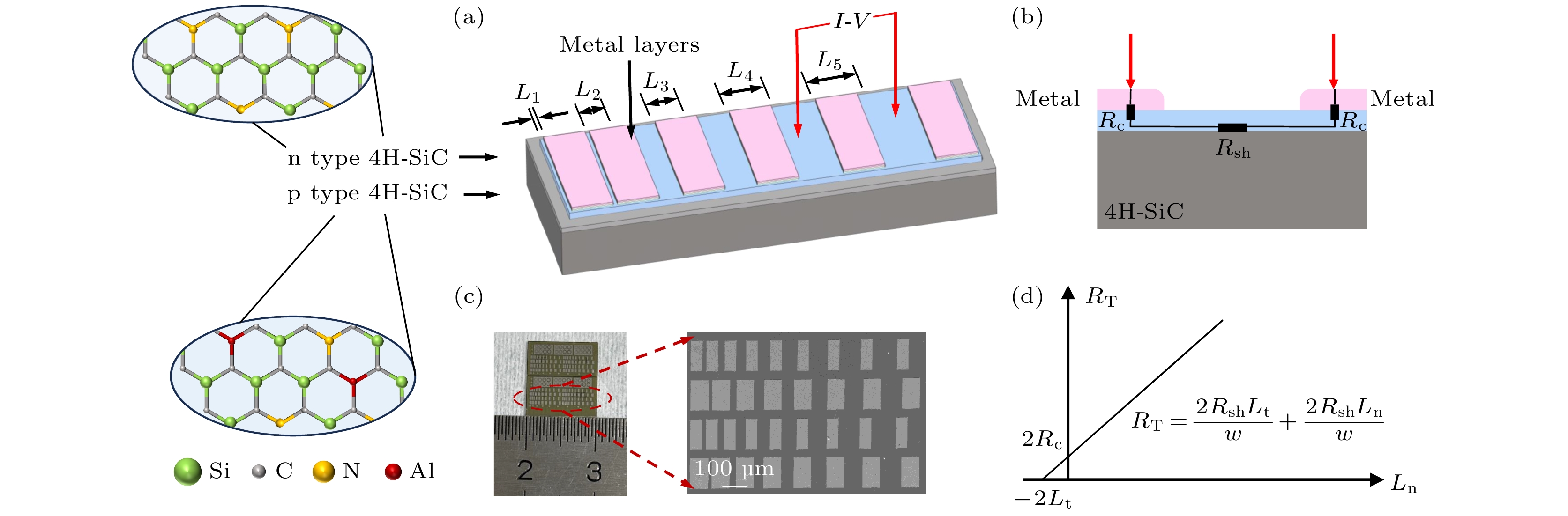
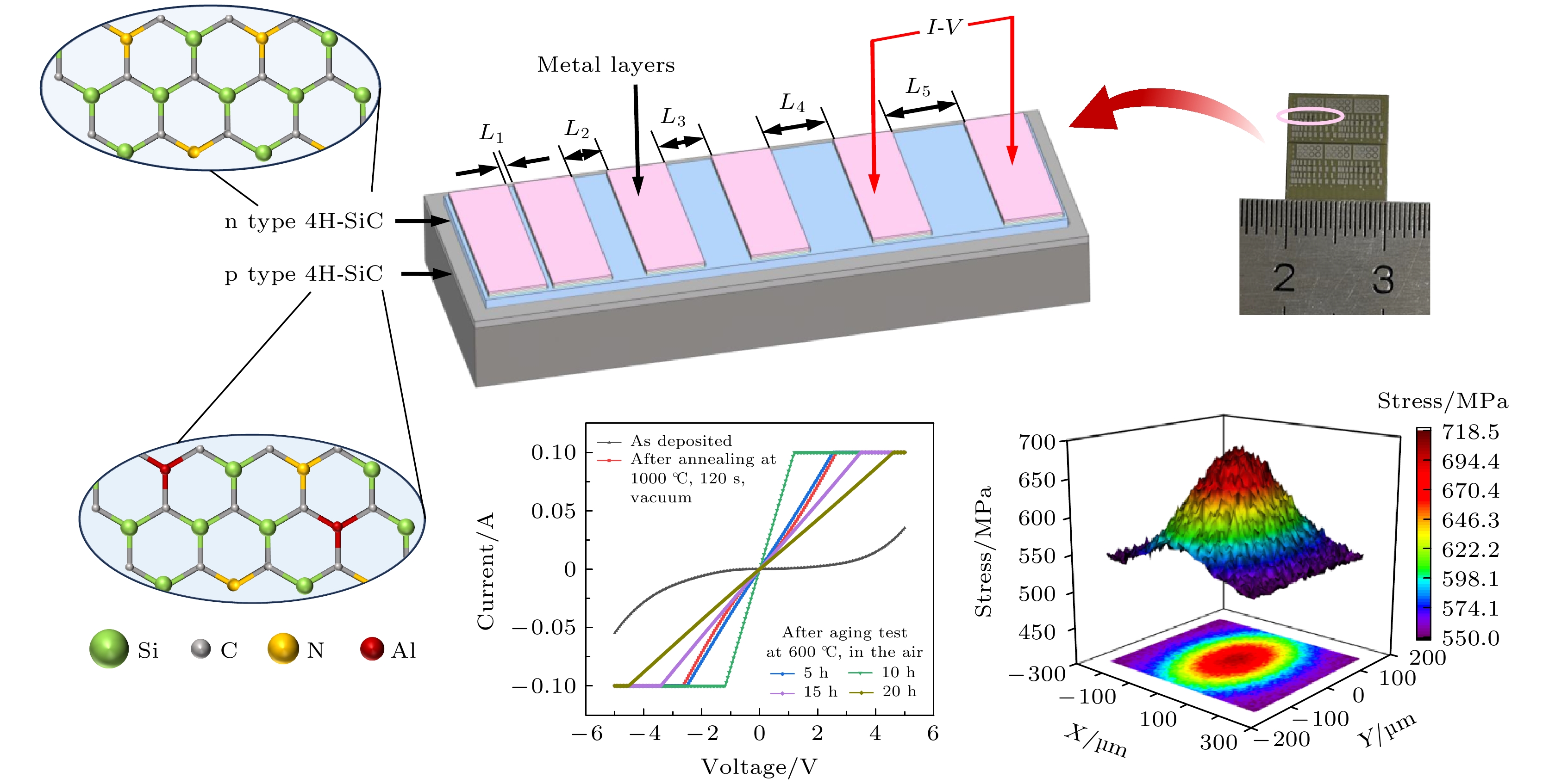
图 1 (a) 4H-SiC NPN型TLM测试方法; (b)TLM等效电极模型; (c) N型4H-SiC的TLM样品; (d) RT - Ln图
Fig. 1. (a) 4H-SiC NPN type TLM test method; (b) equivalent electrical model of the TLM method; (c) the fabricated N type 4H-SiC TLM samples; (d) RT - Ln graph.
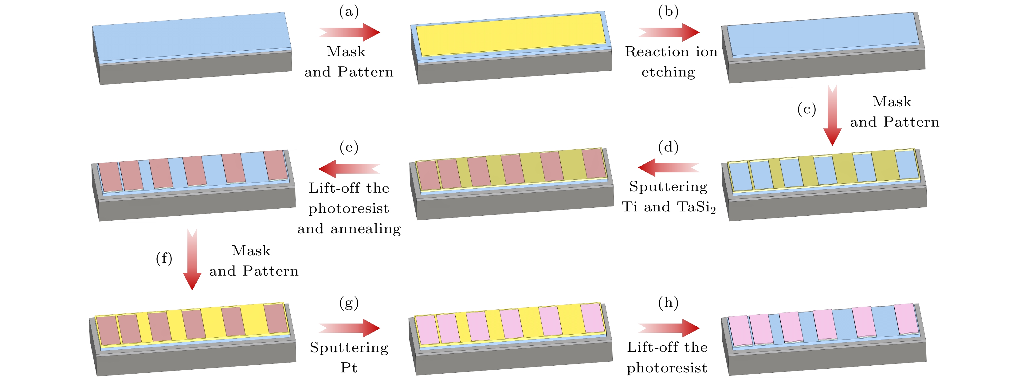
图 2 金属/SiC欧姆接触TLM样品制备流程
Fig. 2. Fabricating processes of metal/SiC ohmic contact TLM samples.
图 3 (a), (b) SiC/Ti/TaSi2/Pt高温退火后表面形貌; (c) SiC/Ti/TaSi2/Pt退火后电极应力分布; (d), (e) SiC/Ti/TaSi2退火后沉积Pt表面形貌; (f) SiC/Ti/TaSi2退火后沉积Pt电极应力分布
Fig. 3. (a), (b) Surface morphology of SiC/Ti/TaSi2/Pt after high-temperature annealing; (c) electrode stress distribution of SiC/Ti/TaSi2/Pt after annealing; (d), (e) surface morphology of SiC/Ti/TaSi2 deposited Pt after annealing; (f) electrode stress distribution of SiC/Ti/TaSi2 deposited Pt after annealing.
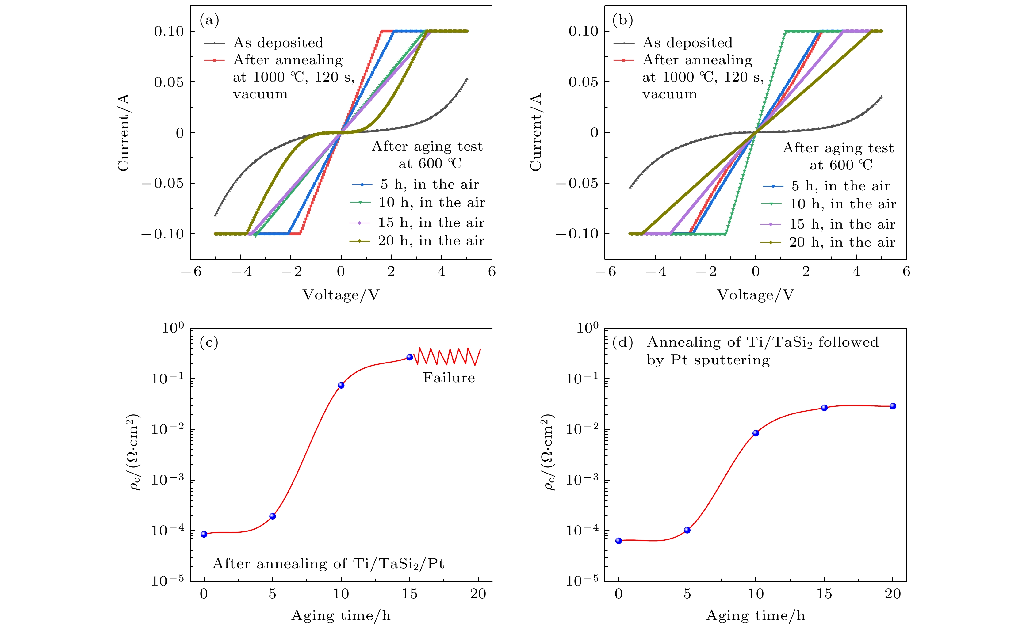
图 4 I-V特性 (a) 组合A(SiC/Ti/TaSi2/Pt); (b) 组合B(SiC/Ti/TaSi2形成欧姆接触后溅射Pt). 比接触电阻率与老化时间的关系 (c) 组合A(SiC/Ti/TaSi2/Pt); (d) 组合B(SiC/Ti/TaSi2形成欧姆接触后溅射Pt)
Fig. 4. I-V characteristics: (a) Combination A(SiC/Ti/TaSi2/Pt); (b) combination B(SiC/Ti/TaSi2 sputtered Pt after forming an ohmic contact). Specific contact resistivity versus aging time: (c) Combination A(SiC/Ti/TaSi2/Pt); (d) combination B(SiC/Ti/TaSi2 sputtered Pt after forming an ohmic contact).
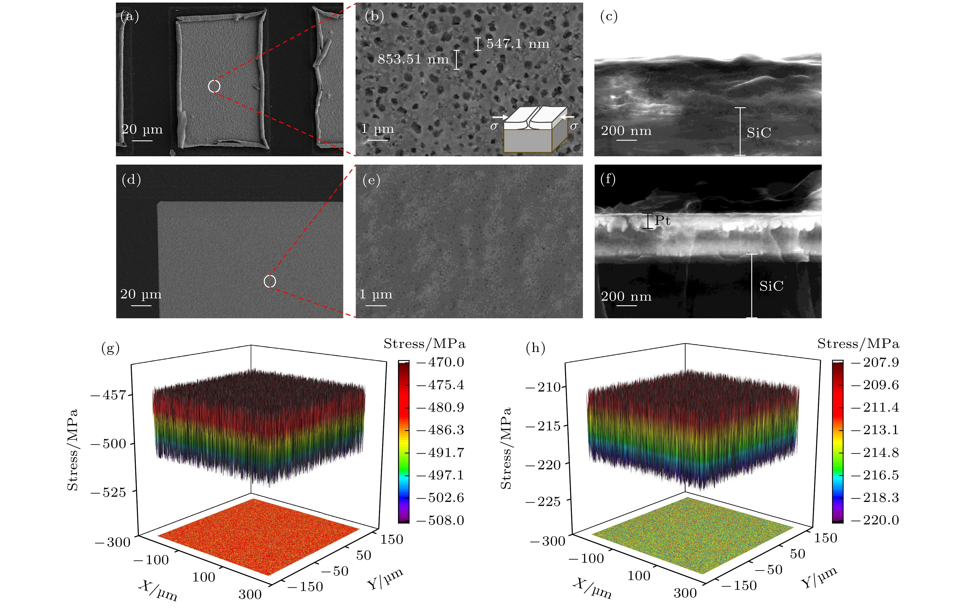
图 5 SiC/Ti/TaSi2/Pt 600 ℃老化20 h后形貌 (a), (b)表面形貌; (c) SEM截面. SiC/Ti/TaSi2退火后沉积Pt 600 ℃老化20 h后形貌 (d), (e)表面形貌; (f) SEM截面. (g) SiC/Ti/TaSi2/Pt 600 ℃老化20 h后电极应力分布; (f) SiC/Ti/TaSi2退火后沉积Pt 600 ℃老化20 h后电极应力分布
Fig. 5. SiC/Ti/TaSi2/Pt morphology after aging at 600 °C for 20 hours: (a), (b) Surface morphology; (c) SEM cross-section. SiC/Ti/TaSi2 annealed followed by Pt deposition, morphology after 600 °C aging for 20 hours: (d), (e) Surface morphology; (f) SEM cross-section. (g) Electrode stress distribution of SiC/Ti/TaSi2/Pt after 600 °C aging for 20 hours. (f) SiC/Ti/TaSi2 annealed and deposited with Pt, after aging at 600 °C for 20 hours, electrode stress distribution.
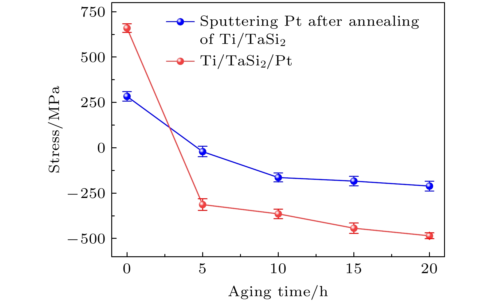
图 6 组合A (Ti/TaSi2/Pt 共溅射退火)与组合B (分批次溅射退火)在600 ℃空气环境下老化不同时间的应力变化趋势
Fig. 6. Stress trends of combination A (Ti/TaSi2/Pt co-sputter annealed) and combination B (batch sputter annealed) aged at 600 °C in air for different time periods.
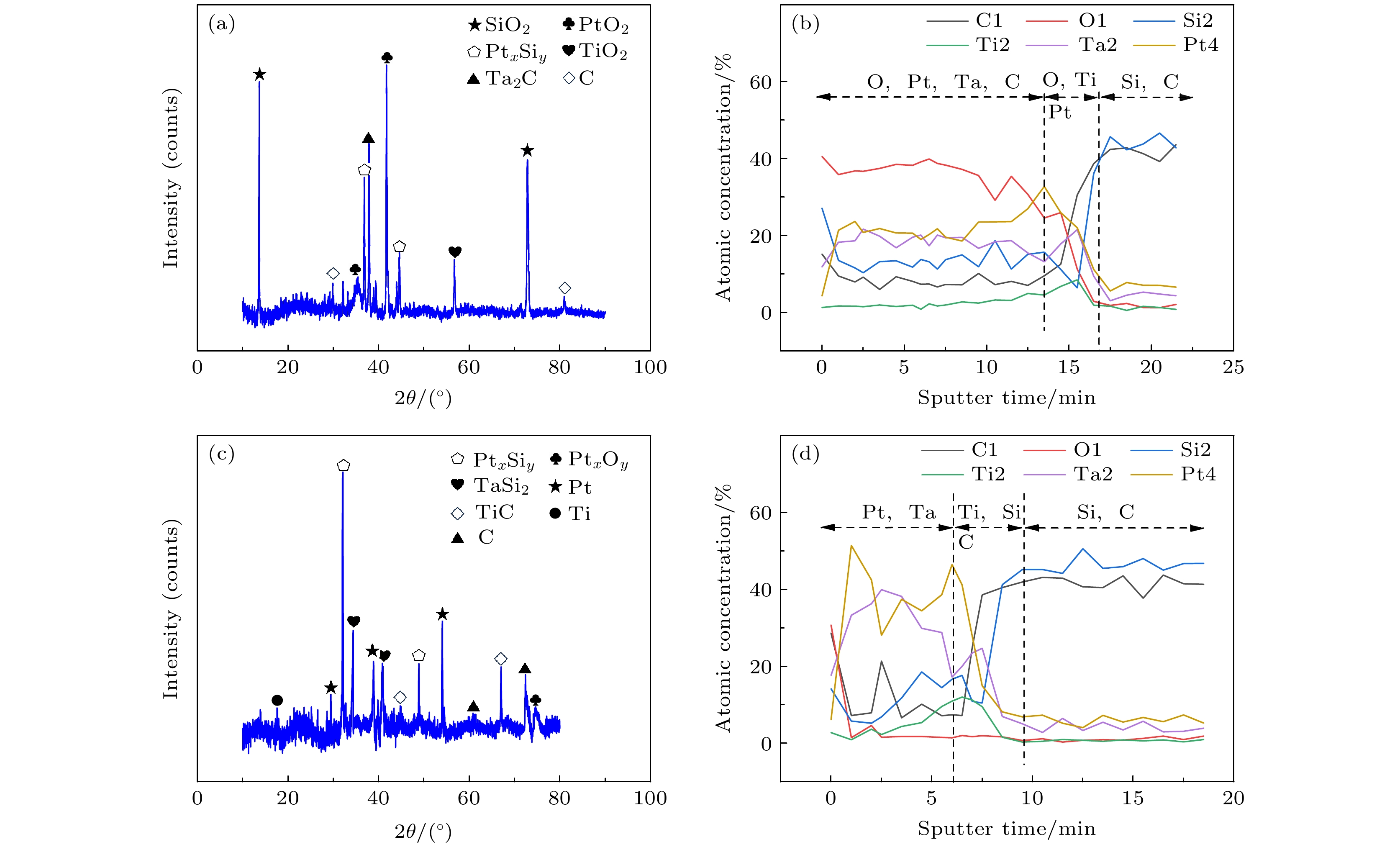
图 7 (a) Ti/TaSi2/Pt共溅射退火老化20 h后的XRD分析; (b) Ti/TaSi2/Pt 共溅射退火的AES分析; (c)分批次溅射退火老化20 h后的XRD分析; (d)分批次溅射退火的AES分析
Fig. 7. (a) XRD analysis after aging for 20 hours of Ti/TaSi2/Pt co-sputtered annealing; (b) AES analysis of Ti/TaSi2/Pt co-sputtered annealing; (c) XRD analysis after aging for 20 hours of batch sputtered annealing; (d) AES analysis of batch sputtered annealing.
-
[1] Wright N G, Horsfall A B 2007 J. Phys. D: Appl. Phys. 40 6345
Google Scholar
[2] 林洪峰, 谢二庆, 马紫微, 张 军, 彭爱华, 贺德衍 2004 物理学报 53 2780
Google Scholar
Lin H F, Xie E Q, Ma Z W, Zhang J, Peng A H, He D Y 2004 Acta Phys. Sin. 53 2780
Google Scholar
[3] 陈建举, 彭淑平, 邓淑玲, 周文, 范志强, 张小姣 2025 物理学报 74 198502
Google Scholar
Chen J J, Peng S P, Deng S L, Zhou W, Fan Z Q, Zhang X J 2025 Acta Phys. Sin. 74 198502
Google Scholar
[4] Anoldo L, Triolo C, Panarello S, Garescì F, Russo S, Messina A A, Calabretta M, Patanè S 2021 IEEE Electron Dev. Lett. 42 1089
Google Scholar
[5] Ding C, Liu H, Ngo K D T, Burgos R, Lu G Q 2021 IEEE Trans. Power Electron. 36 11672
Google Scholar
[6] Li G, Xu M S, Zou D Y, Cui Y X, Zhong Y, Cui P, Cheong K Y, Xia J B, Nie H K, Li S Q, Linewih H, Zhang B T, Xu X G, Han J S 2023 Crystals 13 1106
Google Scholar
[7] Sze S M 2006 Physics of Semiconductor Devices (New York: Wiley) pp335–339
[8] 施敏 著 (赵鹤鸣 译) 2002 半导体器件物理与工艺 (第 2 版) (苏州: 苏州大学出版社) 第226—227页
Shi M (translated by Zhao H M) 2002 Semiconductor Device Physics and Processes (2nd Ed.) (Suzhou: Suzhou University Press) pp226–227
[9] Vivona M, Greco G, Lo Nigro R, Bongiorno C, Roccaforte F 2015 Journal of Applied Physics 118 035705
Google Scholar
[10] Evans L J, Okojie R S, Lukco D 2012 Mater. Sci. Forum 717–720 841
[11] 郭涛 2017 硕士学位论文(西安:西安电子科技大学)
Guo T 2017 M. S. Thesis (Xian: Xidian University
[12] Zhang Q W, Liu Y, Li H F, Wang J, Wang Y, Cheng F B, Han H J, Zhang P 2024 Sensors 24 7731
Google Scholar
[13] Han L B, Liang L, Kang Y, Qiu Y F 2021 IEEE Trans. Power Electron. 36 2080
Google Scholar
[14] He Y J, Lv H L, Tang X Y, Song Q W, Zhang Y M, Han C, Guo T, He X N, Zhang Y M, Zhang Y M 2019 J. Alloys Compd. 805 999
Google Scholar
[15] Liu C Y, Du J F, Rong L M, Luo T C, Gao K, Yin Y G, Xu J 2020 17th China International Forum on Solid State Lighting & 2020 International Forum on Wide Bandgap Semiconductors China (SSLChina: IFWS) Shenzhen, China, November 23–25, 2020 pp247–250
[16] Okojie R S, Lukco D, Chen Y L, Spry D J 2002 J. Appl. Phys. 91 6553
Google Scholar
[17] Wu C, Fang X D, Kang Q, Fang Z Y, Sun H, Zhang D, Zhao L B, Tian B, Maeda R, Jiang Z D 2023 J. Mater. Res. Technol. 24 2428
Google Scholar
[18] Zhang M L, Ren X R, Chu H G, Lv J S, Li W, Wang W G, Yang Q Q, Feng P Z 2020 Corros. Sci. 177 108982
Google Scholar
[19] Zhu H J, Yang T, Zhou Y, Hua S, Yang J W 2019 De Gruyter Brill 74 353
[20] Ng K K, Liu R 1990 IEEE Trans. Electron Dev. 37 1535
Google Scholar
[21] Berger H H 1972 J. Electrochem. Soc. 119 507
Google Scholar
[22] 王印月, 甄聪棉, 龚恒翔, 阎志军, 王亚凡, 刘雪芹, 杨映虎, 何山虎 2000 物理学报 49 1348
Google Scholar
Wang Y Y, Zhen C M, Gong H X, Yan Z J, Wang Y F, Liu X Q, Yang Y H, He S H 2000 Acta Phys. Sin. 49 1348
Google Scholar
[23] Yu S Z, Song Y, Dong J R, Sun Y R, Zhao Y M, He Y 2016 Chin. Phys. B 25 118101
Google Scholar
[24] Scorzoni A, Finetti M 1988 Materials Science Reports 3 79
Google Scholar
[25] Zhou S X, Ai L K, Qi M, Xu A H, Yan J S, Li S S, Jin Z 2021 Chin. Phys. B 30 027304
Google Scholar
[26] Qiao X X, Xia T L, Chen P 2021 Chin. Phys. B 30 018104
Google Scholar
[27] Sha Y C, Li Z W, Jia Z C, Han B, Ni X W 2023 Chin. Phys. B 32 106104
Google Scholar
[28] Huang S S, Zhang X 2006 J. Micromech. Microeng. 16 382
Google Scholar
[29] Han L L, Du C H, Ma Z G, Jiang Y, Xiong K L, Wang W X, Chen H, Deng Z, Jia H Q 2021 Chin. Phys. Lett. 38 068102
Google Scholar
[30] Santerre F, El Khakani M A, Chaker M, Dodelet J P 1999 Appl. Surf. Sci. 148 24
Google Scholar
[31] Kwong D L 1984 Thin Solid Films 121 43
Google Scholar
[32] Yoon D S, Lee S M, Baik H K 2000 J. Electrochem. Soc. 147 3477
Google Scholar

 下载:
下载:
计量
- 文章访问数: 1028
- PDF下载量: 13
- 被引次数: 0
