


-
In this work, gallium oxide (Ga2O3) thin films are deposited on quartz substrates by radio frequency magnetron sputtering at room temperature and annealed in argon atmosphere at different temperatures. The influences of annealing temperatures in the argon atmosphere on crystal structure, transmittance, surface morphology, and optical band gap of the samples are investigated in detail. It is found that the annealing process can improve the crystalline quality of the film, but high-temperature annealing can also easily cause oxygen elements in the film to escape from the film to form oxygen vacancies, which is evidenced by XPS test results. To obtain the effect of the annealing process on the performance of gallium oxide thin film detector, the metal-semiconductor-metal (MSM) photodetector based on the sample annealed at 800 °C, which is compared with untreated sample operated at a reverse bias voltage of 1.1 V, can achieve excellent comprehensive photo-detection properties for 254 nm ultraviolet light: the light-dark current ratio (I254/Idark), responsivity and specific detectivity are as high as 1021.3, 0.106 A/W and 1.61 × 10¹² Jones, respectively, which are 7.5, 195 and 38.3 times those of the unannealed sample device. And the external quantum efficiency is improved by 51.6%. The rise time of sample detector (0.19/0.48 s) annealed at 800 ℃ decreases compared with that of the unannealed sample (0.93/0.93 s), and the descent time of 800 ℃ detector (0.64/0.72 s)increases compared with that of the unannealed sample (0.45/0.49 s), respectively. By comparing the parameters with those of other current gallium oxide-based MSM photodetectors, it is found that the detector parameters of this work have some gaps compared with the current optimal parameters, which is attributed to the fact that the quartz substrate is selected for this work and not the sapphire substrate that is better matching with gallium oxide, resulting in the poor quality of the film compared with that of the sample on the sapphire substrate, and in this work, the photodetector has the high light-dark current ratio (PDCR) and detection rate (D*). In the end, the mechanism of increasing oxygen vacancies after being annealed, which leads to the improvement of detector performance parameters, is analyzed in detail.
-
Keywords:
- gallium oxide /
- RF magnetron sputtering /
- post-annealing temperature /
- solar-blind photodetector
[1] Liu X Z, Guo P, Sheng T, Qian L X, Zhang W L, Li Y R 2016 Opt. Mater. 51 203
 Google Scholar
[2] Xu J J, Zheng W, Huang F 2019 J. Mater. Chem. C 7 8753
Google Scholar
[3] Wang H, Ma J, Cong L, Zhou H, Li P, Fei L, Li B, Xu H, Liu Y 2021 Mater. Today Phys. 20 100464
Google Scholar
[4] Xie C, Lu X T, Liang Y, Chen H H, Wang L, Wu C Y, Wu D, Yang W H, Luo L B 2021 J. Mater. Sci. Technol. 72 189
Google Scholar
[5] Guo X C, Hao N H, Guo D Y, Wu Z P, An Y H, Chu X L, Li L H, Li P G, Lei M, Tang W H 2016 J. Alloys Compd. 660 136
Google Scholar
[6] Lu N Y, Gu Y, Weng Y Y, Da Z C, Ding Y 2019 Mater. Res. Express 6 095033
Google Scholar
[7] Wang L, Gu D W, Shen L J 2017 Solid State Sci. 72 10
Google Scholar
[8] Yu M, Wang H Q, Wei W, Peng B, Yuan L, Hu J C, Zhang Y M, Jia R X 2021 Appl. Surf. Sci. 568 150826
Google Scholar
[9] Ghosh S, Baral M, Kamparath R, Singh S D, Gangul T 2019 Appl. Phys. Lett. 115 251603
Google Scholar
[10] Kaur D, Kumar M 2021 Adv. Opt. Mater. 3 2002160
Google Scholar
[11] Wang D, Ma X C, Xiao H D, Chen R R, Le Yong, Luan C N, Zhang B, Ma J 2022 Mater. Res. Bull. 149 111718
Google Scholar
[12] Mukhopadhyay P, Hatipoglu I, Sakthivel T S, Hunter D A, Edwards P R, Martin R W, Naresh-Kumar G, Seal S, Schoenfeld W V 2021 Adv. Photonics Res. 2 2000067
Google Scholar
[13] Jeong S H, Vu Ti K O, Kim E K 2021 J. Alloys Compd. 877 160291
Google Scholar
[14] Yu M, Lv C D, Yu J G, Shen Y M, Yuan L, Hu J C, Zhang S N, Cheng H J, Zhang Y M, Jia R X 2020 Mater. Today Commun. 25 101532
Google Scholar
[15] Shen H, Yin Y N, Tian K, Baskaran K, Duan L B, Zhao X R, Tiwari A 2018 J. Alloys Compd. 766 601
Google Scholar
[16] Patila V, Lee B T, Jeong S H 2022 J. Alloys Compd. 894 162551
Google Scholar
[17] Li M Q, Yang N, Wang G G, Zhang H Y, Han J C 2019 Appl. Surf. Sci. 471 694
Google Scholar
[18] Zhang Y J, Yan J L, Li Q S, Qu C, Zhang L Y, Li T 2011 Physica B 406 3079
Google Scholar
[19] Goyal A, Yadav B S, Thakur O P, Kapoor A K, Muralidharan R 2014 J. Alloys Compd. 583 214
Google Scholar
[20] Feng Z Q, Huang L, Feng Q, Li X, Zhang H, Tang W h, Zhang J C, Hao Y 2018 Opt. Mater. Express 8 2229
Google Scholar
[21] Tien C H, Hsiao B W, Chen C M, Chen M I, Chiang J L, Wuu D S 2020 Ceram. Int. 46 24147
Google Scholar
[22] Singh A K, Gupta M, Sathe V, Katharria Y S 2021 Superlattice Microst. 156 106976
Google Scholar
[23] Yu J G, Nie Z Z, Dong L P, Yuan L, Li D J, Huang Y, Zhang L C, Zhang Y M, Jia R X 2019 J. Alloys Compd. 798 458
Google Scholar
[24] Wang H Y, Tang C M, Yang W J, Zhao J J, Liu L H, Mu J X, Zhang Y P, Zeng C Y 2022 Ceram. Int. 48 3481
Google Scholar
[25] Cui R R, Zhang J, Luo Z J, Guo X, Ding Z, Deng C Y 2021 Chinese Phys. B 2 028505
Google Scholar
[26] Wei P, Zhu D M, Huang S S, Zhou W C, Luo F 2013 Appl. Surf. Sci. 285P 577
[27] Zhou H T, Cong L J, Ma J G, Chen M Z, Song D Y, Wang H B, Li P, Li B S, Xu H Y, Liu Y C 2020 J. Alloys Compd. 847 156536
Google Scholar
[28] Han J F, Yang D Z, Ma D G, Qiao W Q, Wang Z Y 2019 Org. Electron. 68 242
Google Scholar
[29] Gong. X, Tong M, Xia Y J, Cai W Z, Moon J S, Cao Y, Yu G, Shieh C L, Nilsson B, Heeger A J 2009 Science 325 1665
Google Scholar
[30] 周树仁, 张红, 莫慧兰, 刘浩文, 熊元强, 李泓霖, 孔春阳, 叶利娟, 李万俊 2021 物理学报 70 178503
Google Scholar
Zhou S R, Zhang H, Mo H L, Liu H W, Xiong Y Q, Li H L, Kong C Y, Ye L J, Li W J 2021 Acta Phys. Sin. 70 178503
Google Scholar
[31] Xu R, Ma X C, Chen Y H, Mei Y, Ying L Y, Zhang B P, Long H 2022 Mat. Sci. Semicon. Proc. 144 106621
Google Scholar
[32] Zhou S, Peng X, Liu H W, Zhang Z F, Ye L J, Li H L, Xiong Y Q, Niu L B, Chen F L, Fang L, Kong C Y, Li W J, Yang X, Zhang A H 2022 Opt. Mater. Express 12 327
[33] Wang Q L, Huang P, Liu Q, Li Y X, Qu Q L, Li M K, Homewood K P, Lu Y M, He Y B 2020 J. Alloys Compd. 834 155036
Google Scholar
-
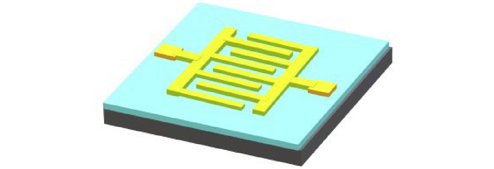
图 1 氧化镓MSM探测器器件结构图
Figure 1. The device structure of the gallium oxide MSM detector.
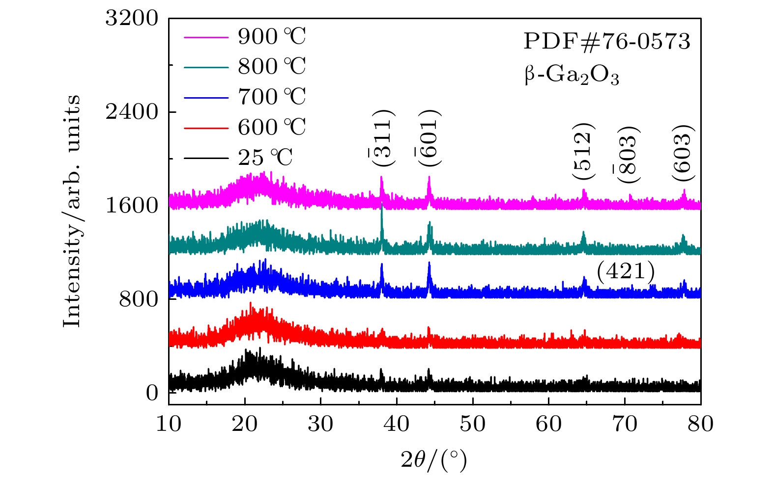
图 2 不同退火温度的XRD图谱
Figure 2. XRD patterns at different annealing temperatures.
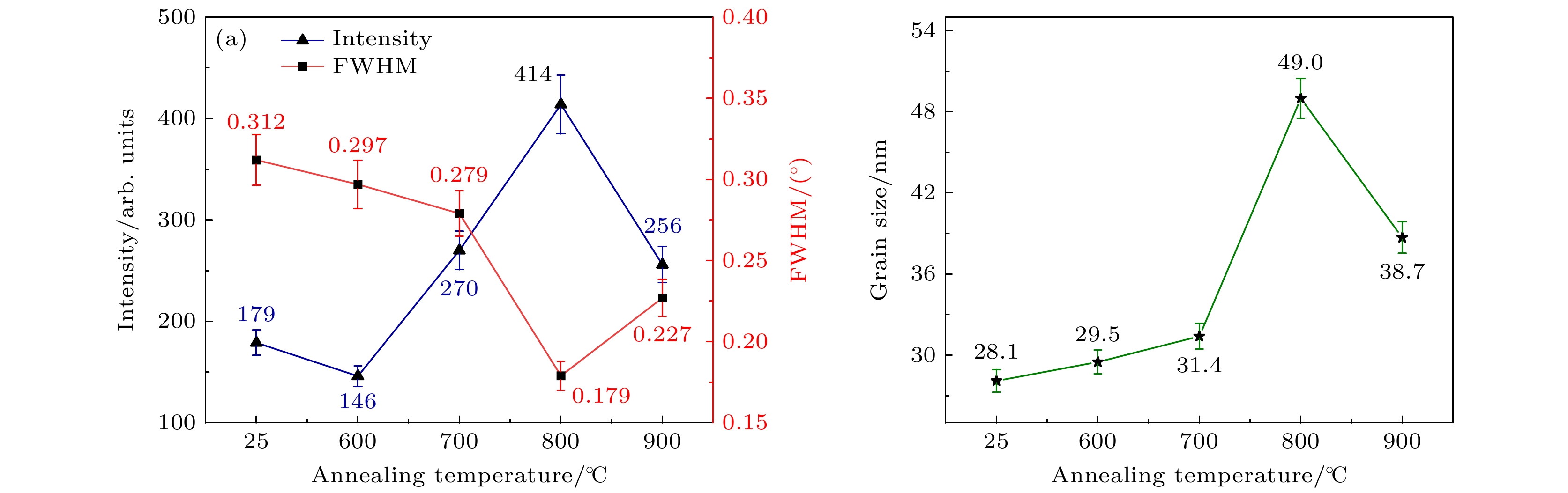
图 3 (a) 不同退火温度下的半峰宽和峰强度图像; (b)不同退火温度的平均晶粒尺寸图像
Figure 3. (a) Images of the half-peak width and peak intensity at different annealing temperatures; (b) images of average grain size at different annealing temperatures.

图 4 退火温度分别为600 ℃ (a), 700 ℃ (b), 800 ℃ (c)和900 ℃ (d)的AFM图像, 以及4个样品的均方根粗糙度图像(e)
Figure 4. AFM images of annealing temperatures of 600 ℃ (a), 700 ℃ (b), 800 ℃ (c) and 900 ℃ (d), and RMS roughness images (e) of the four samples.
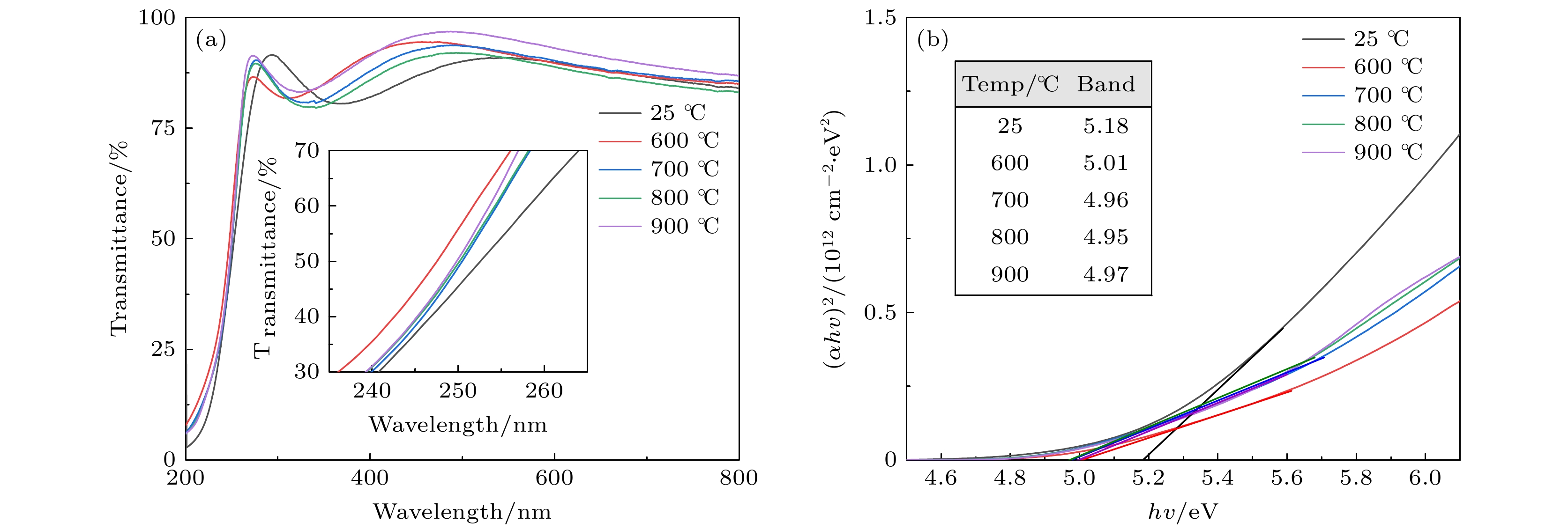
图 5 (a) 不同退火温度下的氧化镓薄膜透射光谱; (b) 不同退火温度薄膜样品光学带隙图像
Figure 5. (a) Transmission spectra of Ga2O3 thin films at different annealing temperatures; (b) optical band gap images of thin films at different annealing temperatures.
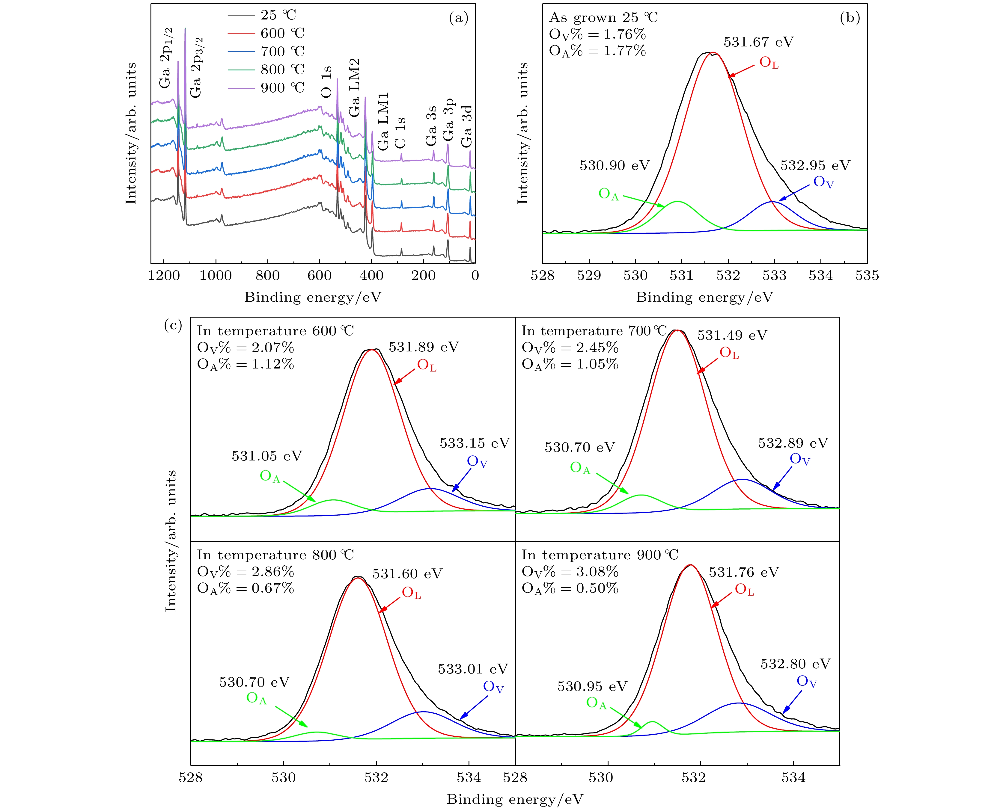
图 6 不同退火温度下薄膜样品的XPS测量全谱 (a) 以及沉积态 (b) 和退火样品 (c) 的O1s精细谱
Figure 6. XPS survey spectra (a) and high-resolution O1s spectra for the as-grown (b), in different annealing temperatures (c) of Ga2O3 film.
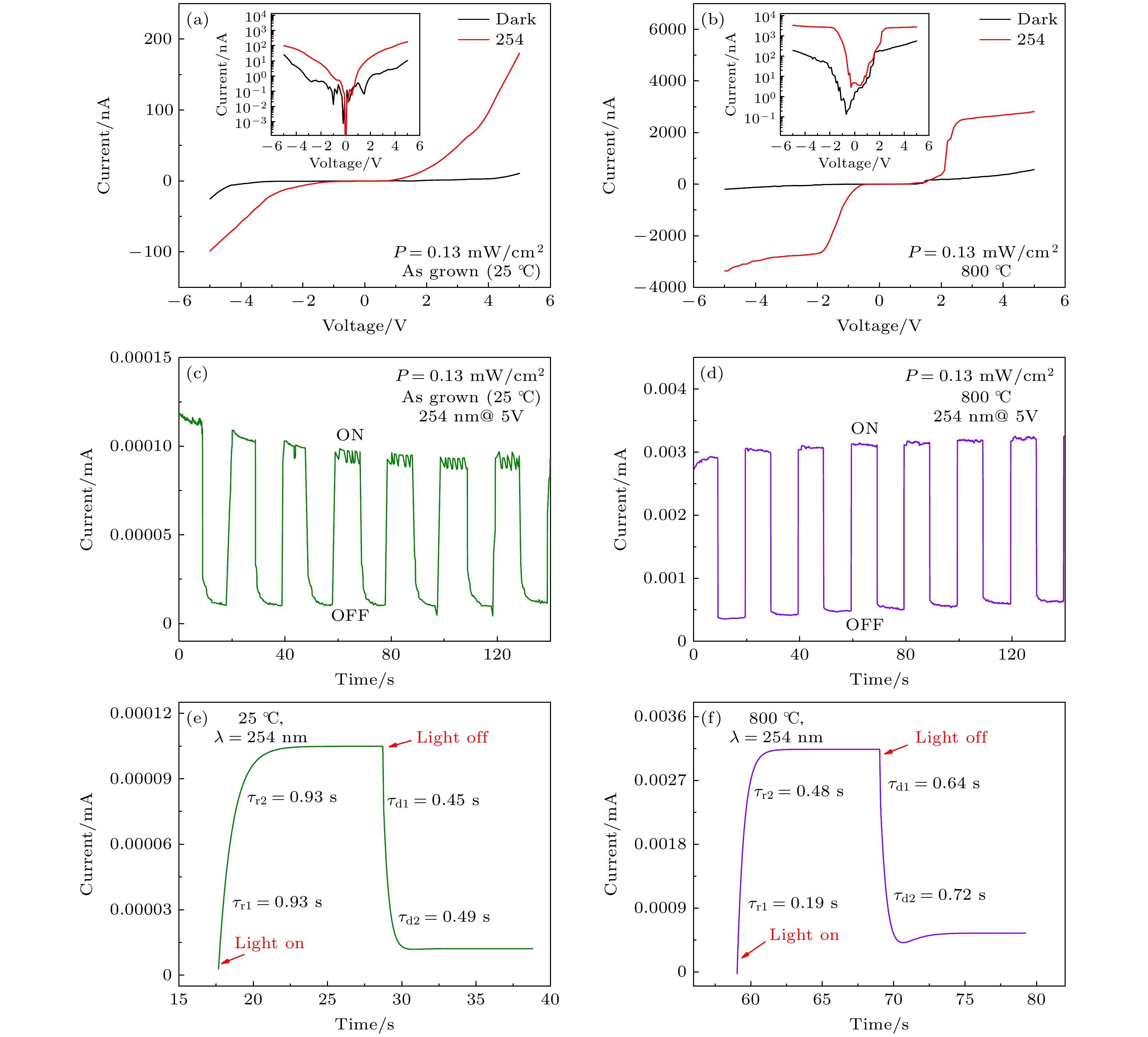
图 7 室温下生长样品 (a) 和800 ℃ 退火样品 (b) 在黑暗环境下及254 nm 紫外光源照射下的I-V图像和半对数图像以及在5 V偏压下, 25 ℃ (c), 800 ℃ (d)的I-T图像及其双指数拟合I-T图像 (e) 和 (f)
Figure 7. I-V images and semi-logarithmic images of samples grown at room temperature (a) and annealed at 800 ℃ (b) in the dark under 254 nm UV light source and under 5 V bias, the I-T image of 25 ℃ (c), 800 ℃ (d) and its bi-exponential fitting I-T images (e), (f).

图 8 光开启时 (a) 和光关闭后 (b) 氧化镓MSM器件能带示意图, 途径1表示光生载流子的产生 (a) 与复合 (b), 途径2表示氧空位缺陷捕获 (a) 和释放 (b) 光生电子
Figure 8. Schematic diagram of the energy band of the gallium oxide MSM device when the light is turned on (a) and after the light is turned off (b). Pathway 1 represents the generation (a) and recombination (b) of photogenerated carriers, and pathway 2 represents oxygen vacancy defect trapping (a) and release (b) photogenerated electrons.
表 1 在5 V偏压下I-T双指数拟合图像响应时间参数表
Table 1. I-T Bi-exponential fitted image response time parameters at 5 V bias.
Photodetector τr1/s τr2/s τd1/s τd2/s 25 ℃ 0.93 0.93 0.45 0.49 800 ℃ 0.19 0.48 0.64 0.72  DownLoad: CSV
表 2 在–1.1 V偏压下的探测器参数汇总表
Table 2. Summary table of detector parameters at –1.1 V bias.
Photodetector Idark/nA PDCR(I254/Idark) Rλ/(A·W–1) EQE/% D*/Jones 25 ℃ 0.0262 136 5.54 × 10⁻⁴ 0.2 4.21 × 10¹⁰ 800 ℃ 0.677 1021.3 0.106 51.8 1.61 × 10¹²
DownLoad: CSV
表 3 当前氧化镓基MSM结构光电探测器主要性能参数汇总表
Table 3. Comparison of main performance parameters of current gallium oxide-based MSM photodetectors
Photodetector Method Id/nA PDCR R254/
(A·W–1)D*/Jones Ref. Ga2O3/Al2O3 Sol-gel 0.125@15 V 673 0.04 4.6 × 10¹¹ [14] Ga2O3/SiC Sputtering 7.6@10 V 383 2.6 1.6 × 10¹² [17] Ga2O3/Al2O3 PLD 0.1@20 V 520 60 — [27] N:Ga2O3/Al2O3 Sputtering 0.01@10 V — 0.013 6.1 × 10¹⁰ [30] Ga2O3/Al2O3 MOCVD 0.17@10 V 4.53 9.4 0.17 × 10¹² [31] Ga2O3/Al2O3 Sputtering 8.2 × 10⁻⁵@10 V 3.58 × 10⁵ 1.93 6.53 × 10¹³ [32] Ga2O3/Quartz Sputtering 0.677@1.1 V 1021.3 0.106 1.61 × 10¹² This work
DownLoad: CSV
-
[1] Liu X Z, Guo P, Sheng T, Qian L X, Zhang W L, Li Y R 2016 Opt. Mater. 51 203
Google Scholar
[2] Xu J J, Zheng W, Huang F 2019 J. Mater. Chem. C 7 8753
Google Scholar
[3] Wang H, Ma J, Cong L, Zhou H, Li P, Fei L, Li B, Xu H, Liu Y 2021 Mater. Today Phys. 20 100464
Google Scholar
[4] Xie C, Lu X T, Liang Y, Chen H H, Wang L, Wu C Y, Wu D, Yang W H, Luo L B 2021 J. Mater. Sci. Technol. 72 189
Google Scholar
[5] Guo X C, Hao N H, Guo D Y, Wu Z P, An Y H, Chu X L, Li L H, Li P G, Lei M, Tang W H 2016 J. Alloys Compd. 660 136
Google Scholar
[6] Lu N Y, Gu Y, Weng Y Y, Da Z C, Ding Y 2019 Mater. Res. Express 6 095033
Google Scholar
[7] Wang L, Gu D W, Shen L J 2017 Solid State Sci. 72 10
Google Scholar
[8] Yu M, Wang H Q, Wei W, Peng B, Yuan L, Hu J C, Zhang Y M, Jia R X 2021 Appl. Surf. Sci. 568 150826
Google Scholar
[9] Ghosh S, Baral M, Kamparath R, Singh S D, Gangul T 2019 Appl. Phys. Lett. 115 251603
Google Scholar
[10] Kaur D, Kumar M 2021 Adv. Opt. Mater. 3 2002160
Google Scholar
[11] Wang D, Ma X C, Xiao H D, Chen R R, Le Yong, Luan C N, Zhang B, Ma J 2022 Mater. Res. Bull. 149 111718
Google Scholar
[12] Mukhopadhyay P, Hatipoglu I, Sakthivel T S, Hunter D A, Edwards P R, Martin R W, Naresh-Kumar G, Seal S, Schoenfeld W V 2021 Adv. Photonics Res. 2 2000067
Google Scholar
[13] Jeong S H, Vu Ti K O, Kim E K 2021 J. Alloys Compd. 877 160291
Google Scholar
[14] Yu M, Lv C D, Yu J G, Shen Y M, Yuan L, Hu J C, Zhang S N, Cheng H J, Zhang Y M, Jia R X 2020 Mater. Today Commun. 25 101532
Google Scholar
[15] Shen H, Yin Y N, Tian K, Baskaran K, Duan L B, Zhao X R, Tiwari A 2018 J. Alloys Compd. 766 601
Google Scholar
[16] Patila V, Lee B T, Jeong S H 2022 J. Alloys Compd. 894 162551
Google Scholar
[17] Li M Q, Yang N, Wang G G, Zhang H Y, Han J C 2019 Appl. Surf. Sci. 471 694
Google Scholar
[18] Zhang Y J, Yan J L, Li Q S, Qu C, Zhang L Y, Li T 2011 Physica B 406 3079
Google Scholar
[19] Goyal A, Yadav B S, Thakur O P, Kapoor A K, Muralidharan R 2014 J. Alloys Compd. 583 214
Google Scholar
[20] Feng Z Q, Huang L, Feng Q, Li X, Zhang H, Tang W h, Zhang J C, Hao Y 2018 Opt. Mater. Express 8 2229
Google Scholar
[21] Tien C H, Hsiao B W, Chen C M, Chen M I, Chiang J L, Wuu D S 2020 Ceram. Int. 46 24147
Google Scholar
[22] Singh A K, Gupta M, Sathe V, Katharria Y S 2021 Superlattice Microst. 156 106976
Google Scholar
[23] Yu J G, Nie Z Z, Dong L P, Yuan L, Li D J, Huang Y, Zhang L C, Zhang Y M, Jia R X 2019 J. Alloys Compd. 798 458
Google Scholar
[24] Wang H Y, Tang C M, Yang W J, Zhao J J, Liu L H, Mu J X, Zhang Y P, Zeng C Y 2022 Ceram. Int. 48 3481
Google Scholar
[25] Cui R R, Zhang J, Luo Z J, Guo X, Ding Z, Deng C Y 2021 Chinese Phys. B 2 028505
Google Scholar
[26] Wei P, Zhu D M, Huang S S, Zhou W C, Luo F 2013 Appl. Surf. Sci. 285P 577
[27] Zhou H T, Cong L J, Ma J G, Chen M Z, Song D Y, Wang H B, Li P, Li B S, Xu H Y, Liu Y C 2020 J. Alloys Compd. 847 156536
Google Scholar
[28] Han J F, Yang D Z, Ma D G, Qiao W Q, Wang Z Y 2019 Org. Electron. 68 242
Google Scholar
[29] Gong. X, Tong M, Xia Y J, Cai W Z, Moon J S, Cao Y, Yu G, Shieh C L, Nilsson B, Heeger A J 2009 Science 325 1665
Google Scholar
[30] 周树仁, 张红, 莫慧兰, 刘浩文, 熊元强, 李泓霖, 孔春阳, 叶利娟, 李万俊 2021 物理学报 70 178503
Google Scholar
Zhou S R, Zhang H, Mo H L, Liu H W, Xiong Y Q, Li H L, Kong C Y, Ye L J, Li W J 2021 Acta Phys. Sin. 70 178503
Google Scholar
[31] Xu R, Ma X C, Chen Y H, Mei Y, Ying L Y, Zhang B P, Long H 2022 Mat. Sci. Semicon. Proc. 144 106621
Google Scholar
[32] Zhou S, Peng X, Liu H W, Zhang Z F, Ye L J, Li H L, Xiong Y Q, Niu L B, Chen F L, Fang L, Kong C Y, Li W J, Yang X, Zhang A H 2022 Opt. Mater. Express 12 327
[33] Wang Q L, Huang P, Liu Q, Li Y X, Qu Q L, Li M K, Homewood K P, Lu Y M, He Y B 2020 J. Alloys Compd. 834 155036
Google Scholar

 DownLoad:
Catalog
Metrics
- Abstract views: 10849
- PDF Downloads: 237
- Cited By: 0
