


-
Solar-blind UV photodetectors (SBPs) have attracted great attention because they are widely used in missile tracking, fire detection, biochemical analysis, astronomical observations, space-to-space communications, etc. At present, it is found that wide bandgap semiconductor materials such as AlxGa1-xN, Mg1Zn1-xO, diamond and β-Ga2O3 are ideal semiconductor materials for developing high-performance SBPs. The ultra-wide band gap semiconductor material, β-Ga2O3, has a large band gap width of 4.9 eV, strong breakdown electric field, absorption edge located in the solar blind ultraviolet band (200–280 nm), and it also has high transmittance in the near ultraviolet and the whole visible band. Therefore, β-Ga2O3 is a very suitable material for making solar blind UV photodetectors. However, the p-type β-Ga2O3 is difficult to dope, which limits the further development of β-Ga2O3 devices. In this work, the β-Ga2O3 thin films with different Cu doping content are grown on sapphire substrates by chemical vapor deposition method, and the morphology, crystal structure and optical properties of β-Ga2O3 films are measured. The test results show that the surfaces of β-Ga2O3 films with different Cu content are relatively smooth, and the (
$ \bar 201 $ ) diffraction peak positions shift toward the lower degree side with the increase of Cu content, which indicates that Cu2+ replaces Ga3+ and enters into the β-Ga2O3 lattice. The optical absorption spectrum measurement indicates that the energy gaps of samples are evidently narrowed with the increase of Cu doping concentration. Hall measurements indicate that the Cu doped β-Ga2O3 thin films have a p-type conductivity with a hole concentration of 7.36 × 10¹⁴, 4.83 × 10¹⁵ and 1.69 × 1016 cm–3, respectively. In addition, a photoconductive UV detector with metal-semiconductor-metal structure is prepared by evaporating Au on a Cu-doped β-Ga2O3 thin film, and its UV detection performance is studied. The results show that the photocurrent value of the device increases with Cu content increasing. The photo-to-dark current ratio (Il/Id) is about 3.8×10² of 2.4% Cu content device under 254 nm-wavelength light at 10 V. The rise time and decay time are 0.11 s and 0.13 s, respectively. Furthermore, the responsivity and external quantum efficiency can reach 1.72 A/W and 841% under 254 nm-wavelength light with a light intensity of 64 μW/cm2.-
Keywords:
- chemical vapor deposition /
- p-type β-Ga2O3 /
- Cu doping /
- UV photodetector
[1] 谢自力, 张荣, 修向前, 韩平, 刘斌, 陈琳, 俞慧强, 江若琏, 施毅, 郑有炓 2007 物理学报 56 6717
 Google Scholar
Xie Z L, Zhang R, Xiu X Q, Han P, Liu B, Chen L, Yu H Q, Jiang R L, Shi Y, Zheng Y D 2007 Acta Phys. Sin. 56 6717
Google Scholar
[2] Zhang C X, Xu C B, Wen G J, Lian Y F 2018 Opt. Eng. 57 053109
[3] Alaie Z, Nejad S M, Yousefi M H 2014 J. Mater. Sci. Mater. Electron. 25 852
Google Scholar
[4] Ouyang W, Teng F, Jiang M M, Fang X S 2017 Small 13 1702177
Google Scholar
[5] Fan M M, Liu K W, Zhang Z Z, Li B H, Chen X, Zhao D X, Shan C X, Shen D Z 2014 Appl. Phys. Lett. 105 011117
Google Scholar
[6] Cicek E, McClintock R, Cho C Y, Rahnema B, Razeghi M 2013 Appl. Phys. Lett. 103 191108
Google Scholar
[7] Pearton S J, Yang J C, IV P H C, Ren F, Kim J, Tadjer M J, Mastro M A 2018 Appl. Phys. Rev. 5 011301
Google Scholar
[8] Jubu P R, Yam F K 2020 Sens. Actuators A 312 112141
Google Scholar
[9] Jin C, Park S, Kim H, Lee C 2012 Sens. Actuators B 161 223
Google Scholar
[10] Qian Y P, Guo D Y, Chu X L, Shi H Z, Zhu W K, Wang K, Huang X K, Wang H, Wang S L, Li P G, Zhang X H, Tang W H 2017 Mater. Lett. 209 558
Google Scholar
[11] Wang D, Ge K, Meng D, Chen Z 2023 Mater. Lett. 330 133251
Google Scholar
[12] Zhang C, Li Z, Wang W 2021 Materials 14 5161
Google Scholar
[13] 冯秋菊, 李芳, 李彤彤, 李昀铮, 石博, 李梦轲, 梁红伟 2018 物理学报 67 218101
Google Scholar
Feng Q J, Li F, Li T T, Li Y Z, Shi B, Li M K, Liang H W 2018 Acta Phys. Sin. 67 218101
Google Scholar
[14] Feng Q J, Dong Z J, Liu W, Liang S, Yi Z Q, Yu C, Xie J Z, Song Z 2022 Micro Nanostruct. 167 207255
Google Scholar
[15] Xu C, Shen L, Liu H, Pan X, Ye Z 2021 J. Electron. Mater. 50 2043
Google Scholar
[16] Liu Z, Wang X, Liu Y, Guo D, Li S, Yan Z, Tan C K, Li W, Li P, Tang W 2019 J. Mater. Chem. C 7 13920
Google Scholar
[17] Guo X C, Hao N H, Guo D Y, Wu Z P, An Y H, Chu X L, Li L H, Li P G, Lei M, Tang W H 2016 J. Alloy. Comp. 660 136
Google Scholar
[18] Lin R C, Zheng W, Zhang D, Zhang Z J, Liao Q X, Yang L, Huang F 2018 ACS Appl. Mater. Interfaces 10 22419
Google Scholar
[19] Dong L P, Pang T Q, Yu J G, Wang Y C, Zhu W G, Zheng H D, Yu J H, Jia R X, Zhe C 2019 J. Mater. Chem. C 7 14205
Google Scholar
[20] Chu S Y, Yeh T H, Lee C T, Lee H Y 2022 Mater. Sci. Semicond. Process. 142 106471
Google Scholar
[21] 落巨鑫, 高红丽, 邓金祥, 任家辉, 张庆, 李瑞东, 孟雪 2023 物理学报 72 028502
Google Scholar
Luo J X, Gao H L, Deng J X, Ren J H, Zhang Q, Li R D, Meng X 2023 Acta Phys. Sin. 72 028502
Google Scholar
-
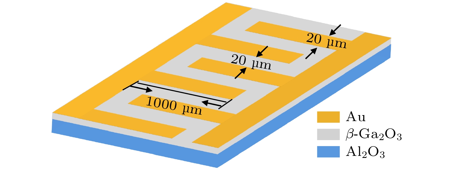
图 1 Cu掺杂β-Ga2O3薄膜日盲紫外探测器结构示意图
Figure 1. Structural diagram of solar-blind ultraviolet detector based on Cu-doped β-Ga2O3 thin film.
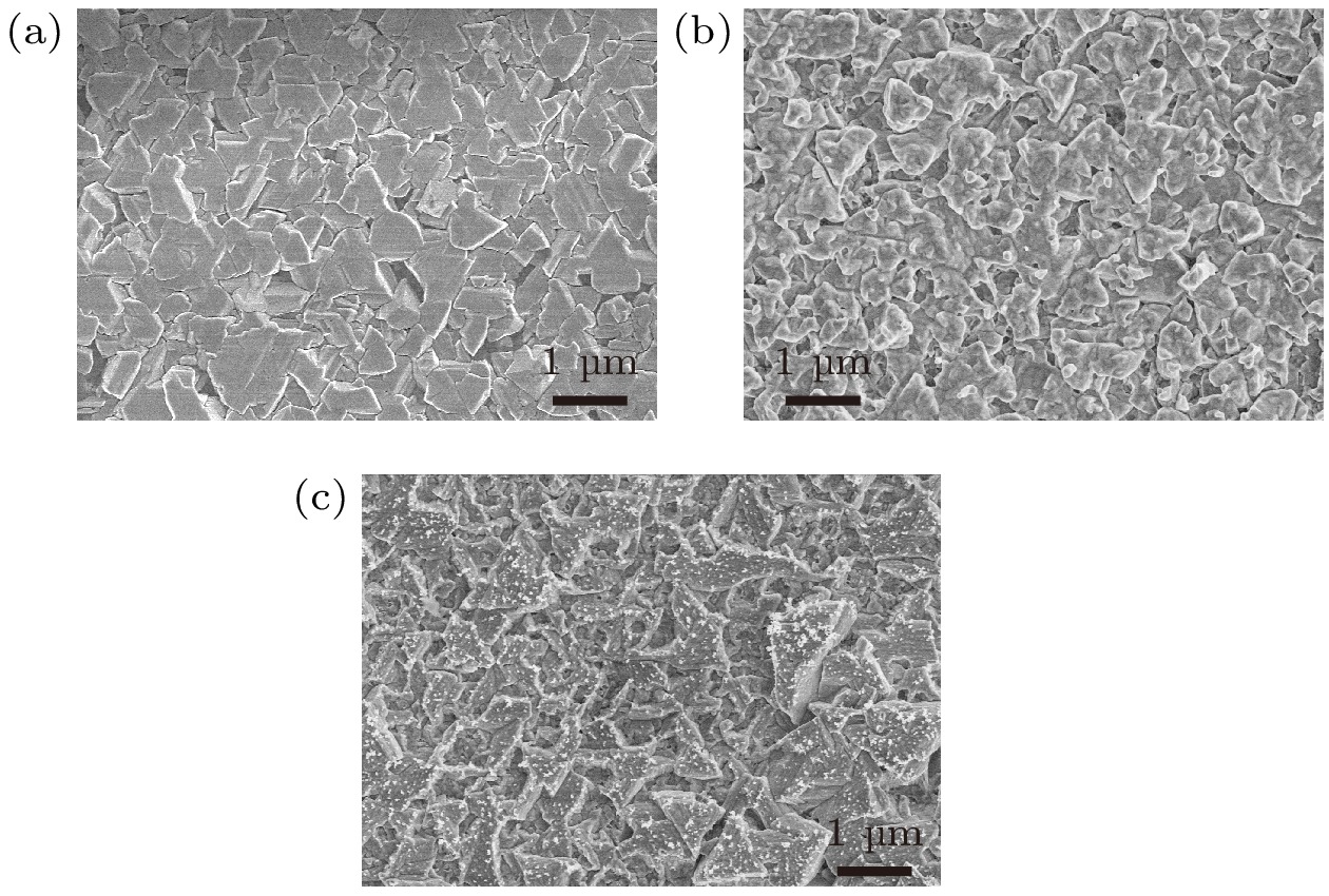
图 2 样品的SEM图 (a)样品A; (b)样品B; (c)样品C
Figure 2. SEM images of samples: (a) Sample A; (b) sample B; (c) sample C.

图 3 样品的EDS能谱图 (a)样品A; (b)样品B; (c)样品C
Figure 3. EDS spectra of samples: (a) Sample A; (b) sample B; (c) sample C.

图 4 (a)样品A, B, C的XRD图谱; (b)样品A, B, C放大的(
$\bar 201 $ )衍射峰的XRD图谱Figure 4. (a) XRD patterns of samples A, B, C; (b) XRD patterns of amplified (
$\bar 201 $ ) diffraction peak of samples A, B, C.
图 5 样品A, B, C的光学吸收图
Figure 5. Absorption spectra of samples A, B, C.

图 6 在黑暗和波长254 nm光照时, 器件的I-V曲线 (a)器件A; (b)器件B; (c)器件C
Figure 6. I-V curves of devices at dark and wave length of 254 nm illumination: (a) Device A; (b) device B; (c) device C.

图 7 (a) 10 V偏压下, 器件C对波长254 nm紫外光在不同光功率密度下的响应I-t曲线; (b)器件C单个周期的响应-恢复时间曲线
Figure 7. (a) I-t curves of responses of device C under wave length of 254 nm UV light at different light intensities at 10 V bias; (b) response-recovery time curves of a cycle for device C.

图 8 器件C的响应度和EQE随光功率密度的变化
Figure 8. Responsivity and EQE of device C with optical power intensity.
表 1 不同Cu掺杂量β-Ga2O3的实验参数
Table 1. Experimental parameters of β-Ga2O3 with different Cu contents.
样品 Ga2O3/CuO
质量比生长温度
/℃反应时间
/minAr流量
/(mL⋅min–1)O2流量
/(mL⋅min–1)A 25∶1 1000 30 200 50 B 25∶2 1000 30 200 50 C 25∶3 1000 30 200 50  DownLoad: CSV
表 2 样品A, B, C的电学性质
Table 2. Electrical properties of sample A, B, C.
样品 导电类型 载流子浓度/cm–3 霍尔迁移率/
(cm2⋅(V⋅s)–1)A p 7.36×10¹⁴ 11.64 B p 4.83×10¹⁵ 7.38 C p 1.69×10¹⁶ 4.52
DownLoad: CSV
-
[1] 谢自力, 张荣, 修向前, 韩平, 刘斌, 陈琳, 俞慧强, 江若琏, 施毅, 郑有炓 2007 物理学报 56 6717
Google Scholar
Xie Z L, Zhang R, Xiu X Q, Han P, Liu B, Chen L, Yu H Q, Jiang R L, Shi Y, Zheng Y D 2007 Acta Phys. Sin. 56 6717
Google Scholar
[2] Zhang C X, Xu C B, Wen G J, Lian Y F 2018 Opt. Eng. 57 053109
[3] Alaie Z, Nejad S M, Yousefi M H 2014 J. Mater. Sci. Mater. Electron. 25 852
Google Scholar
[4] Ouyang W, Teng F, Jiang M M, Fang X S 2017 Small 13 1702177
Google Scholar
[5] Fan M M, Liu K W, Zhang Z Z, Li B H, Chen X, Zhao D X, Shan C X, Shen D Z 2014 Appl. Phys. Lett. 105 011117
Google Scholar
[6] Cicek E, McClintock R, Cho C Y, Rahnema B, Razeghi M 2013 Appl. Phys. Lett. 103 191108
Google Scholar
[7] Pearton S J, Yang J C, IV P H C, Ren F, Kim J, Tadjer M J, Mastro M A 2018 Appl. Phys. Rev. 5 011301
Google Scholar
[8] Jubu P R, Yam F K 2020 Sens. Actuators A 312 112141
Google Scholar
[9] Jin C, Park S, Kim H, Lee C 2012 Sens. Actuators B 161 223
Google Scholar
[10] Qian Y P, Guo D Y, Chu X L, Shi H Z, Zhu W K, Wang K, Huang X K, Wang H, Wang S L, Li P G, Zhang X H, Tang W H 2017 Mater. Lett. 209 558
Google Scholar
[11] Wang D, Ge K, Meng D, Chen Z 2023 Mater. Lett. 330 133251
Google Scholar
[12] Zhang C, Li Z, Wang W 2021 Materials 14 5161
Google Scholar
[13] 冯秋菊, 李芳, 李彤彤, 李昀铮, 石博, 李梦轲, 梁红伟 2018 物理学报 67 218101
Google Scholar
Feng Q J, Li F, Li T T, Li Y Z, Shi B, Li M K, Liang H W 2018 Acta Phys. Sin. 67 218101
Google Scholar
[14] Feng Q J, Dong Z J, Liu W, Liang S, Yi Z Q, Yu C, Xie J Z, Song Z 2022 Micro Nanostruct. 167 207255
Google Scholar
[15] Xu C, Shen L, Liu H, Pan X, Ye Z 2021 J. Electron. Mater. 50 2043
Google Scholar
[16] Liu Z, Wang X, Liu Y, Guo D, Li S, Yan Z, Tan C K, Li W, Li P, Tang W 2019 J. Mater. Chem. C 7 13920
Google Scholar
[17] Guo X C, Hao N H, Guo D Y, Wu Z P, An Y H, Chu X L, Li L H, Li P G, Lei M, Tang W H 2016 J. Alloy. Comp. 660 136
Google Scholar
[18] Lin R C, Zheng W, Zhang D, Zhang Z J, Liao Q X, Yang L, Huang F 2018 ACS Appl. Mater. Interfaces 10 22419
Google Scholar
[19] Dong L P, Pang T Q, Yu J G, Wang Y C, Zhu W G, Zheng H D, Yu J H, Jia R X, Zhe C 2019 J. Mater. Chem. C 7 14205
Google Scholar
[20] Chu S Y, Yeh T H, Lee C T, Lee H Y 2022 Mater. Sci. Semicond. Process. 142 106471
Google Scholar
[21] 落巨鑫, 高红丽, 邓金祥, 任家辉, 张庆, 李瑞东, 孟雪 2023 物理学报 72 028502
Google Scholar
Luo J X, Gao H L, Deng J X, Ren J H, Zhang Q, Li R D, Meng X 2023 Acta Phys. Sin. 72 028502
Google Scholar
-
[1] Su Ran, Xi Zhao-Ying, Li Shan, Zhang Jia-Han, Jiang Ming-Ming, Liu Zeng, Tang Wei-Hua. GaSe/β-Ga2O3 heterojunction based self-powered solar-blind ultraviolet photoelectric detector. Acta Physica Sinica, 2024, 73(11): 118502. doi: 10.7498/aps.73.20240267 [2] Yi Zi-Qi, Wang Yan-Ming, Wang Shuo, Sui Xue, Shi Jia-Hui, Yang Yi-Han, Wang De-Yu, Feng Qiu-Ju, Sun Jing-Chang, Liang Hong-Wei. Performance of UV photodetector of mechanical exfoliation prepared PEDOT:PSS/β-Ga2O3 microsheet heterojunction. Acta Physica Sinica, 2024, 73(15): 157102. doi: 10.7498/aps.73.20240630 [3] Dong Dian-Meng, Wang Cheng, Zhang Qing-Yi, Zhang Tao, Yang Yong-Tao, Xia Han-Chi, Wang Yue-Hui, Wu Zhen-Ping. Ga2O3-based metal-insulator-semiconductor solar-blind ultraviolet photodetector with HfO2 inserting layer. Acta Physica Sinica, 2023, 72(9): 097302. doi: 10.7498/aps.72.20222222 [4] Zhang Mao-Lin, Ma Wan-Yu, Wang Lei, Liu Zeng, Yang Li-Li, Li Shan, Tang Wei-Hua, Guo Yu-Feng. Investigation of high-temperature performance of WO3/β-Ga2O3 heterojunction deep-ultraviolet photodetectors. Acta Physica Sinica, 2023, 72(16): 160201. doi: 10.7498/aps.72.20230638 [5] Guo Yue, Sun Yi-Ming, Song Wei-Dong. Narrowband near-ultraviolet photodetector fabricated from porous GaN/CuZnS heterojunction. Acta Physica Sinica, 2022, 71(21): 218501. doi: 10.7498/aps.71.20220990 [6] Xuan Xin-Miao, Wang Jia-Heng, Mao Yan-Qi, Ye Li-Juan, Zhang Hong, Li Hong-Lin, Xiong Yuan-Qiang, Fan Si-Qiang, Kong Chun-Yang, Li Wan-Jun. Flexible transparent solar blind ultraviolet photodetector based on amorphous Ga2O3 grown on mica substrate. Acta Physica Sinica, 2021, 70(23): 238502. doi: 10.7498/aps.70.20211039 [7] Zhou Shu-Ren, Zhang Hong, Mo Hui-Lan, Liu Hao-Wen, Xiong Yuan-Qiang, Li Hong-Lin, Kong Chun-Yang, Ye Li-Juan, Li Wan-Jun. Effect of N-doping on performance of ${\boldsymbol\beta}$ -Ga2O3 thin film solar-blind ultraviolet detector. Acta Physica Sinica, 2021, 70(17): 178503. doi: 10.7498/aps.70.20210434[8] Wang Wen-Xun, Ren Yan-Biao, Zhang Shi-Chao, Zhang Lin-Cai, Qi Jing-Bo, He Xiao-Wu. Preparation of three-dimensional graphene foam with controllable defects by closed-environment chemical vapor deposition method and composite electrode electrochemical performance. Acta Physica Sinica, 2020, 69(14): 148101. doi: 10.7498/aps.69.20200454 [9] Wang Wen-Jie, Kang Zhi-Lin, Song Qian, Wang Xin, Deng Jia-Jun, Ding Xun-Lei, Che Jian-Tao. Effect of layer variation on the electronic structure of stacked MoS2(1-x) Se2x alloy. Acta Physica Sinica, 2018, 67(24): 240601. doi: 10.7498/aps.67.20181494 [10] Huang Jing-Wen, Luo Li-Qiong, Jin Bo, Chu Shi-Jin, Peng Ru-Fang. Synthesis and photoluminescence property of hexangular star MoSe2 bilayer. Acta Physica Sinica, 2017, 66(13): 137801. doi: 10.7498/aps.66.137801 [11] Yang Yun-Chang, Wu Bin, Liu Yun-Qi. Synthesis of bilayer graphene via chemical vapor deposition and its optoelectronic devices. Acta Physica Sinica, 2017, 66(21): 218101. doi: 10.7498/aps.66.218101 [12] Wu Xiao-Ping, Liu Jin-Yang, Lin Li-Mei, Zheng Wei-Feng, Qu Yan, Lai Fa-Chun. Preparation and characteristics of ZnO nanoflowers. Acta Physica Sinica, 2015, 64(20): 207802. doi: 10.7498/aps.64.207802 [13] Pei Jia-Nan, Jiang Da-Yong, Tian Chun-Guang, Guo Ze-Xuan, Liu Ru-Sheng, Sun Long, Qin Jie-Ming, Hou Jian-Hua, Zhao Jian-Xun, Liang Qing-Cheng, Gao Shang. Effect of Pt NPs in the film on the performances of ZnO-based metal-semiconductor-metal structured ultraviolet photodetector. Acta Physica Sinica, 2015, 64(6): 067802. doi: 10.7498/aps.64.067802 [14] Han Lin-Zhi, Zhao Zhan-Xia, Ma Zhong-Quan. Process parameters of large single crystal graphene prepared by chemical vapor deposition. Acta Physica Sinica, 2014, 63(24): 248103. doi: 10.7498/aps.63.248103 [15] Yuan Ze, Gao Hong, Xu Ling-Ling, Chen Ting-Ting, Lang Ying. Fabrication of In-Al codoped ZnO nanobunches photodetectors. Acta Physica Sinica, 2012, 61(5): 057201. doi: 10.7498/aps.61.057201 [16] Yang Fan, Ma Jin, Kong Ling-Yi, Luan Cai-Na, Zhu Zhen. Structural, optical and electrical properties of Ga2(1-x)In2xO3 films prepared by metalorganic chemical vapor deposition. Acta Physica Sinica, 2009, 58(10): 7079-7082. doi: 10.7498/aps.58.7079 [17] Wu Ding-Cai, Hu Zhi-Gang, Duan Man-Yi, Xu Lu-Xiang, Liu Fang-Shu, Dong Cheng-Jun, Wu Yan-Nan, Ji Hong-Xuan, Xu Ming. Synthesis and photoluminescence of (Co, Cu)-doped ZnO thin films. Acta Physica Sinica, 2009, 58(10): 7261-7266. doi: 10.7498/aps.58.7261 [18] Jin Ke-Xin, Zhao Sheng-Gui, Chen Chang-Le. Photoinduced effect in Cu doping La0.67Sr0.33Cux Mn1-xO3 thin films. Acta Physica Sinica, 2009, 58(7): 4953-4957. doi: 10.7498/aps.58.4953 [19] Li Bao-He, Feng Chun, Yang Tao, Zhai Zhong-Hai, Teng Jiao, Yu Guang-Hua, Zhu Feng-Wu. The effect of Cu doping on the ordering of FexPt1-x thin films. Acta Physica Sinica, 2006, 55(5): 2567-2571. doi: 10.7498/aps.55.2567 [20] Peng Xing-Ping, Lan Wei, Tan Yong-Sheng, Tong Li-Guo, Wang Yin-Yue. Photoluminescent properties of Cu-doped ZnO thin films. Acta Physica Sinica, 2004, 53(8): 2705-2709. doi: 10.7498/aps.53.2705


 DownLoad:


Catalog
Metrics
- Abstract views: 6744
- PDF Downloads: 132
- Cited By: 0
