Vol. 70, No. 16 (2021)
2021-08-20
INVITED REVIEW

EDITOR'S SUGGESTION
2021, 70 (16): 160702.
doi: 10.7498/aps.70.20210685
Abstract +
Laser spectroscopy based techniques have the advantages of high sensitivities, high selectivities, non-invasiveness and in situ, real-time observations. They are widely used in numerous fields, such as environmental monitoring, life science, medical diagnostics, manned space flight, and planetary exploration. Owing to the merits of low cost, compact volume and strong environment adaptability, quartz-enhanced photoacoustic spectroscopy (QEPAS) based sensing is an important laser spectroscopy-based method of detecting the trace gas, which was invented in 2002. Detection sensitivity is a key parameter for gas sensors because it determines their real applications. In this paper, focusing on the detection sensitivity, the common methods for QEPAS are summarized. High power laser including amplified diode laser by erbium doped fiber amplifier (EDFA), and quantum cascade laser are used to improve the excitation intensity of acoustic wave. The absorption line of gas molecules located at the fundamental bands of mid-infrared region is adopted to increase the laser absorption strength. Micro-resonator is employed to enhance the generated acoustic pressure by forming a standing wave cavity. Quartz tuning forks (QTFs) with low resonant frequency are used to increase the accumulation time of acoustic energy in itself. Multi-pass strategy is utilized to amplify the action length between laser beam and target gas in the prongs of QTF. The advantages and disadvantages of the above methods are discussed respectively. For the issues in real applications, the all-fiber strucure in near-infared region and mid-infrared region and miniaturization using three-dimensional(3D) printing technique for QEPAS sensor are summarized. A QEPAS technique based multi-gas sensor is used to quantify the concentration of carbon monoxide (CO), carbon dioxide (CO2), hydrogen cyanide (HCN), and hydrogen chloride (HCl) for post-fire cleanup aboard spacecraft, which is taken for example for the real application.Finally, the methods of further improving the sensitivity of QEPAS sensor are proposed.
GENERAL
2021, 70 (16): 160301.
doi: 10.7498/aps.70.20201981
Abstract +
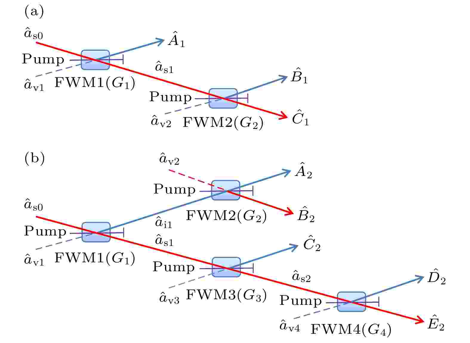
Multipartite quantum steering is an important quantum resource and the basis of secure quantum communication network. Multipartite quantum steering can be generated by beam splitter networks, optical frequency comb systems and nonlinear processes. Different types of quantum steering will be produced by different projects. In this paper, we design two different schemes, i.e. series cascaded four-wave mixing and hybrid cascaded four-wave mixing, and based on these two schemes tripartite quantum steering and quinquepartite quantum steering are generated respectively. The steering characters among different users are quantified based on the covariance matrix. In theory, we investigate steering parameters among different modes created by two schemes versus the amplitude gain of four-wave mixing process. We find that one mode can steer the other two modes separately, but the other two modes cannot steer the one mode simultaneously. By comparing the steering characters of joint multimodes to a certain single mode with the individual mode to the single mode respectively, it can be seen that the steerability of the former is stronger than the latter in the whole gain region, and there exists only the steering of joint multimodes to a single mode in the partial gain region. More importantly, the steerability of joint multimodes to a single mode can be enhanced with the quantity of joint multimodes increasing. The results show that multiple types of quantum steering can be realized by using these two schemes, which are helpful in understanding the distribution of quantum steering in multipartite system and have important significance in practical secure quantum communication and quantum secret sharing.
COVER ARTICLE
2021, 70 (16): 160302.
doi: 10.7498/aps.70.20210648
Abstract +
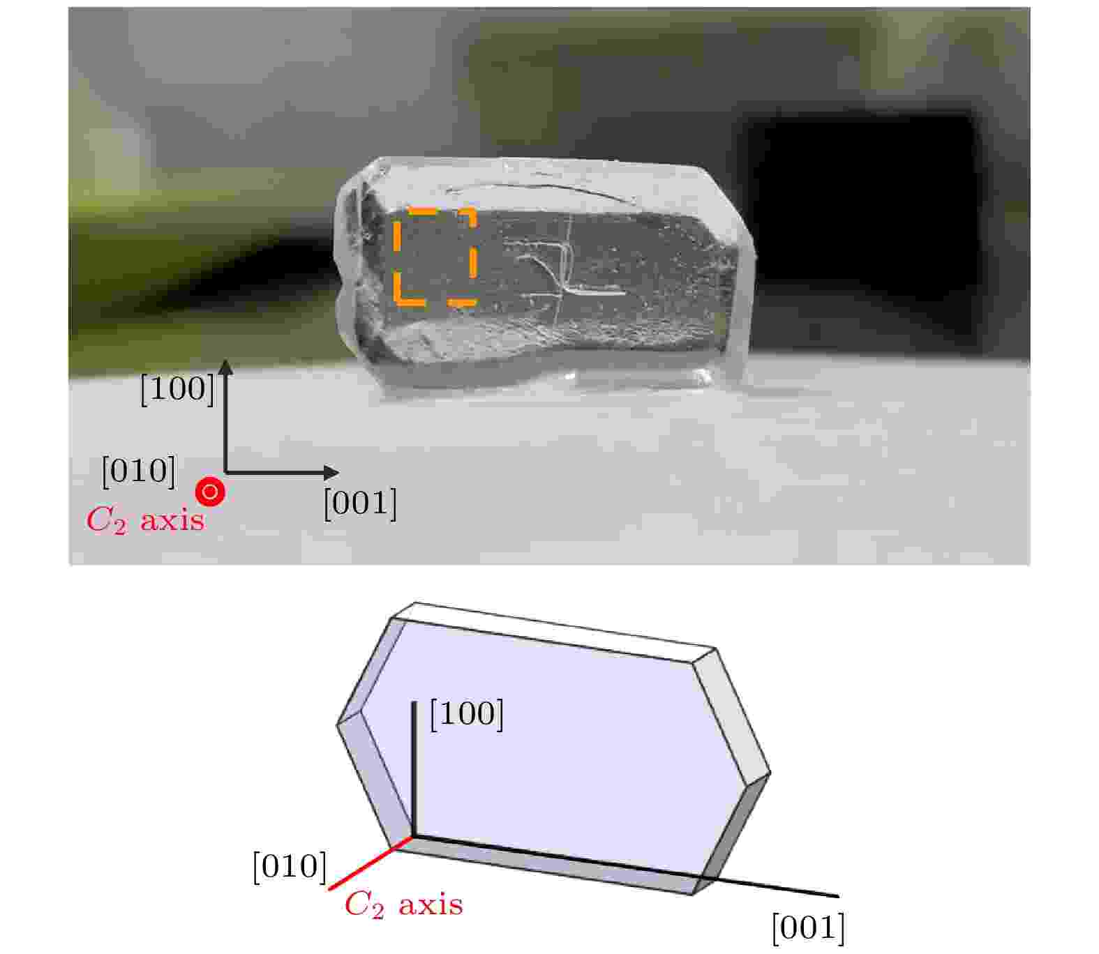
Quantum memory is a crucial component for the large-scale quantum networks. Rare-earth-ion doped crystals have been a promising candidate for the practical quantum memory because of its very long coherence time. However, doped ions cause unwanted lattice distortion, and consequently reduce the optical depth and the storage efficiency. The stoichiometric rare-earth crystals have low lattice distortion and high rare earth ion density, and thus are expected to enable high-efficiency storage. EuCl3·6H2O is a promising material for quantum memory applications because its optical inhomogeneous broadening can be smaller than its hyperfine splitting and the theoretically predicted spin coherence time is up to 1000 seconds. Despite the numerous efforts in solid-state quantum memory based on rare-earth ion doped crystals, optical memory and quantum memory have not been implemented with stoichiometric rare-earth crystals yet. Here, we report the atom frequency comb optical storage using a EuCl3·6H2O crystal. A coherence time of 55.7 μs is obtained by photon echo measurements on $^7{\rm{F}}_0 \rightarrow {}^5{\rm{D}}_0$ transition. The two-level atomic frequency comb storage is demonstrated with a storage efficiency of 1.71% at a storage time of 1 μs, showing the potential capability of optical quantum storage of this material. Based on the analysis of the line shift of $^7{\rm{F}}_0 \rightarrow {}^5{\rm{D}}_0$ depending on the sample temperature, we highlight the challenge of achieving high-efficiency optical pumping in this material, which imposes a limit on the achievable efficiency.
2021, 70 (16): 160701.
doi: 10.7498/aps.70.20210247
Abstract +
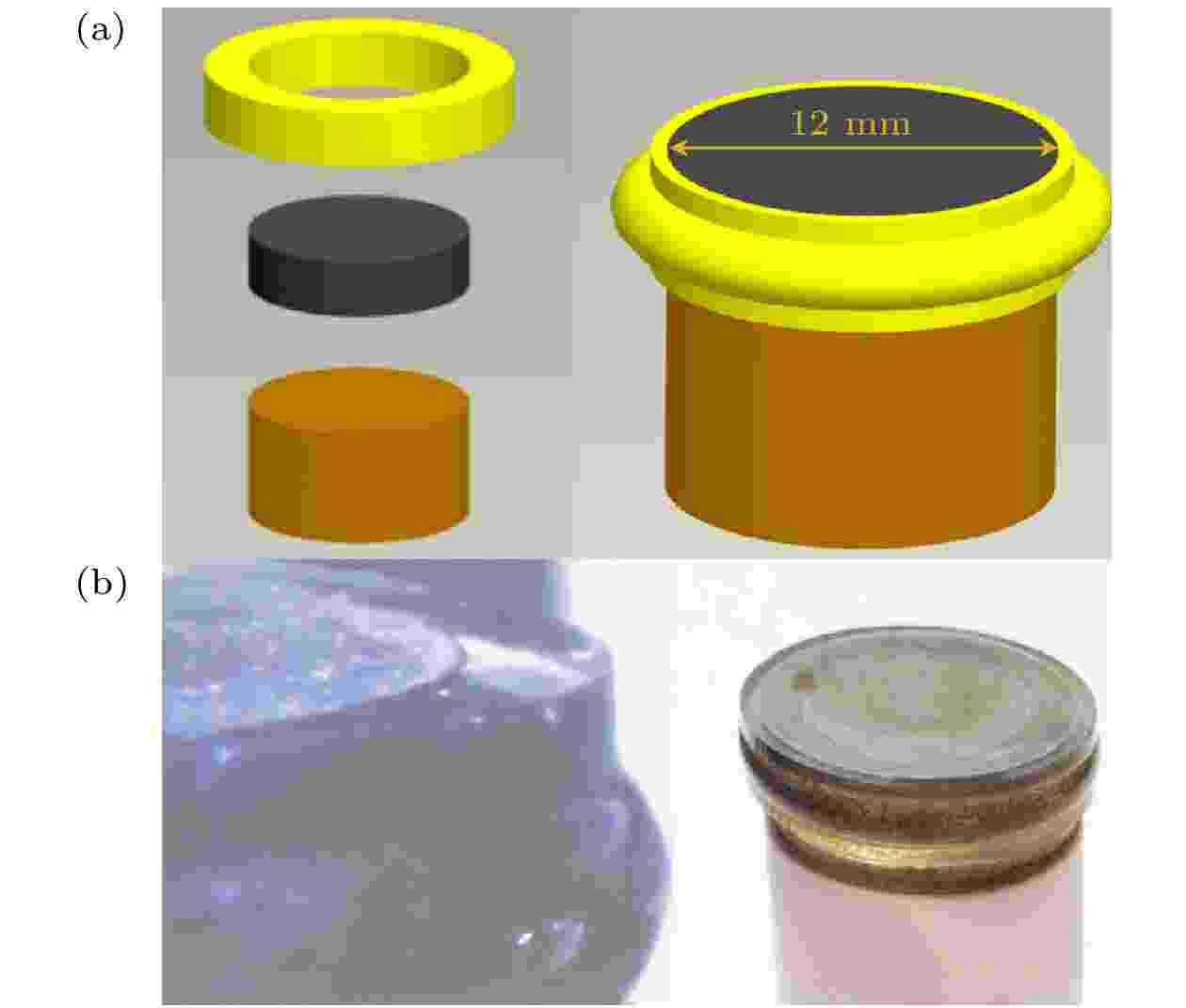
Applications of magnetometers are affected mainly by their sensitivities and detection bandwidths. Till now, the applications of the centimeter-scale optomechanical magnetometer have been still limited by those two factors. In order to improve its sensing performance in a low frequency regime of the alternating current (AC) magnetic field sensor based on centimeter-scale whispering gallery mode resonator, we design a new centimeter-scale crystalline whispering gallery mode resonator which has different relative distributions of the magnetostrictive material (Terfenol-D) and the optical material (CaF2) from the unoptimized centimeter-scale whispering gallery mode resonator. Experimental results show that this new resonator is able to detect the AC magnetic field ranging from 6 Hz to 1 MHz, and a peak sensitivity of 530 pT·Hz–1/2 at 123.8 kHz is achieved without DC bias field in a magnetically unshielded non-cryogenic environment. On condition that the optical quality factor is at the same level of 108 and there is no DC bias magnetic field, the best sensitivity of the optimized resonator is 11 times higher than that of the unoptimized resonator, and the corresponding detection frequency band is expanded by 1.67 times, switching from the frequency band of 10 Hz–600 kHz to 6 Hz–1 MHz. Besides, the device only needs 100 μW light intensity to operate, which offers us a low optical power consumption magnetometer. Within the detection frequency band, the proposed magnetometer can detect both a single frequency alternating magnetic field signal and an alternating magnetic field signal covering a certain frequency range. It can detect 50 or 60 Hz alternating magnetic field signal generated by current in the wire so that the working status of the power system can be monitored. If the sensing performance is further improved, it may be able to detect the magnetic field signal at frequency in a range of 1 kHz–10 MHz generated by the partial discharge current and the extremely low frequency human body magnetic field signal located in a frequency band of [10 mHz–1 kHz]. Further improvement in sensing performance is possible through optimizing the system noise and the magnetic field response capability of the device, which might allow the device to possess the applications in the fields of power system fault monitoring and medical diagnosis.
2021, 70 (16): 160703.
doi: 10.7498/aps.70.20210029
Abstract +
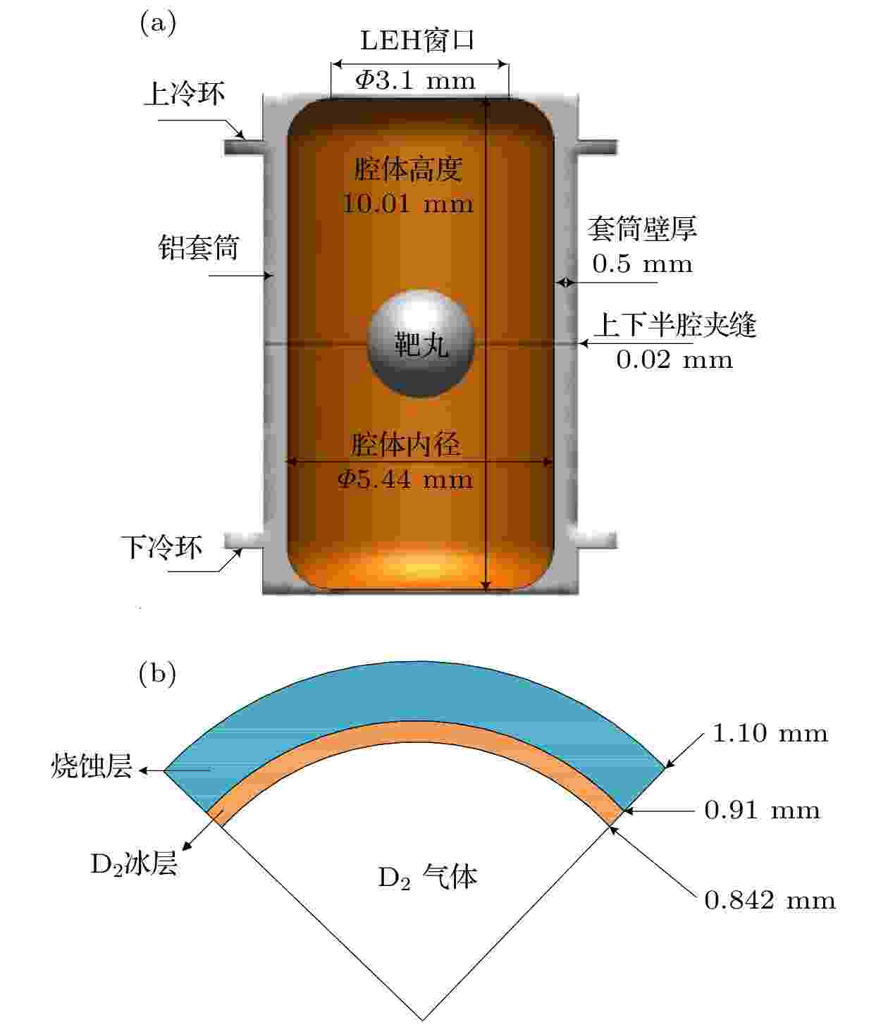
For an inertial-confinement-fusion cryogenic target, the fusion ice layer inside the capsule should have a uniformity more than 99% and an inner surface roughness less than 1 μm (root mean square) to avoid Rayleigh-Taylor instabilities. And this highly smooth ice layer required for ignition is generated at the presence of volumetric heat and affected by the thermal environment around the capsule. For the D2 fuel targets, the volumetrically heating can be supplied by exposing the ice layer to IR radiation. A major challenge of IR-layering is a spherically uniform IR illumination of the capsule, particularly for capsules held in cylindrical hohlraums in indirect-drive targets. In the present study, a numerical study is conducted on the thermal environment of D2 fuel capsule under directional infrared radiation. A 3D simulation model coupling the photonic and thermal fields has been established based on the Monte Carlo ray tracing method. The influence of infrared optical fibers’ layouts and source power intensity on temperature characteristics outside the capsule have been studied. The results indicate that at constant total power of optical fibers, the more optical fibers set up, the lower the average temperature of the outer surface decreases, and the more uniform the capsule outer surface temperature turns to be. The temperature uniformity of capsule outer surface deteriorates with the two or less optical fibers, but improves with the number greater than 2 in which case ΔTmax and ΔTw can decrease by 61.94% and 76.33% at most. A proper offset of optical fiber spots towards the hohlraum poles can improve the temperature uniformity of capsule outer surface, while the other two optical fiber spot offset schemes deteriorate the temperature uniformity. The results are of guiding significance for determining the optical fibers layout in experiment and further design option for cryogenic targets.
EDITOR'S SUGGESTION
2021, 70 (16): 160704.
doi: 10.7498/aps.70.20210156
Abstract +
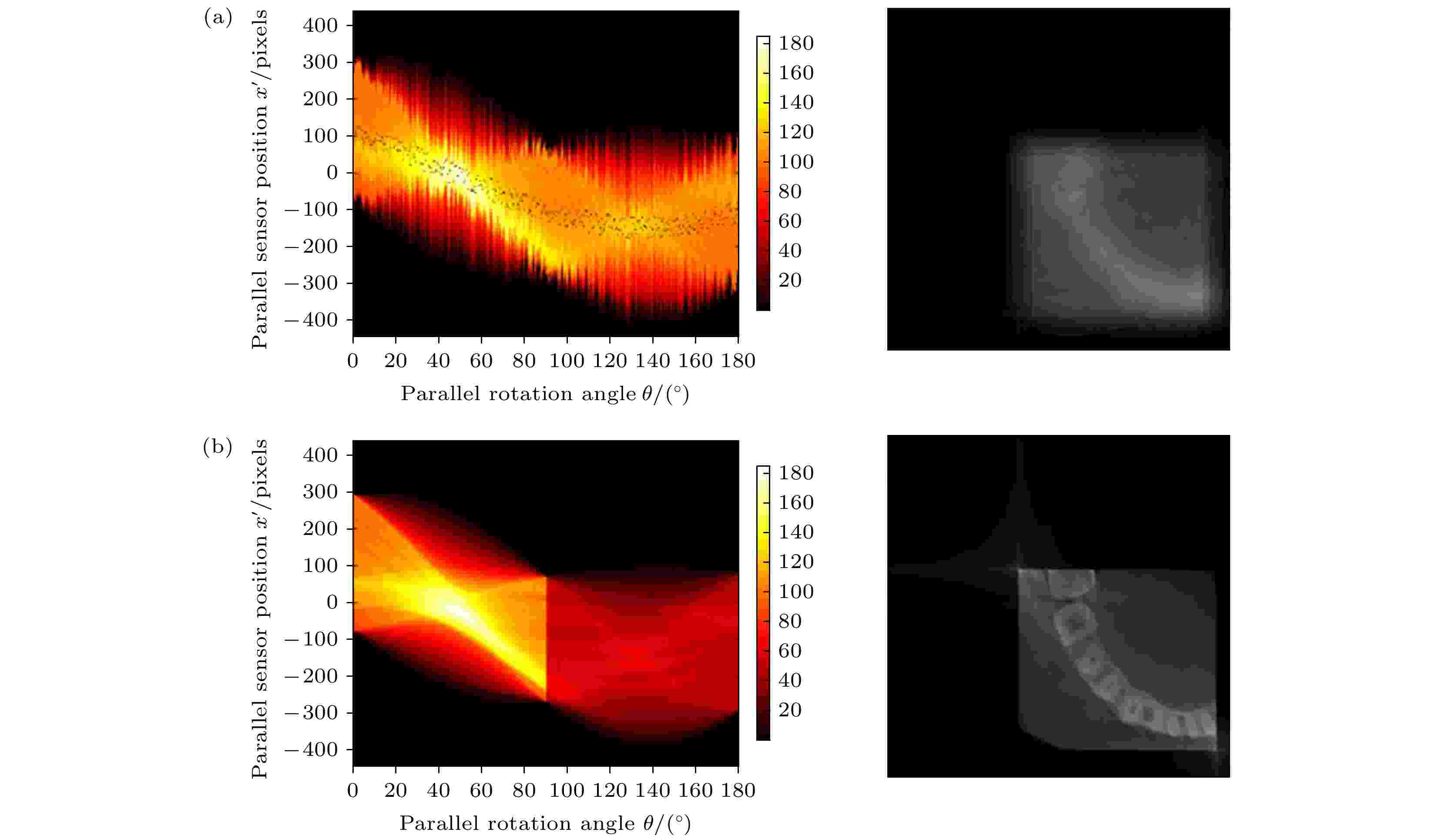
Synchrotron radiation-based X-ray nano-imaging is a powerful tool for non-destructively studying the internal nano-scale structure of matter. Here in this paper, we review the state-of-the-art image alignment technology in the field of nano-resolution imaging, and classify and analyze the technology according to the research stage. First, through the publications of image alignment algorithm, the development direction of future research is analyzed. Then, the most effective image alignment application in the field of nano imaging based on classic image alignment algorithms is summarized. The paper also presents the feature detection operators that are useful for nano-scale image registration selected from recent feature detection research, which has important guiding significance for the specific application and optimization of nano-imaging image registration. Finally, the state-of-the-art image registration method based on deep learning is introduced, the applicability and potential of deep learning in nano-imaging registration technology are discussed, and future research directions and challenges are prospected based on different neural network characteristics.
THE PHYSICS OF ELEMENTARY PARTICLES AND FIELDS
2021, 70 (16): 161201.
doi: 10.7498/aps.70.20210030
Abstract +
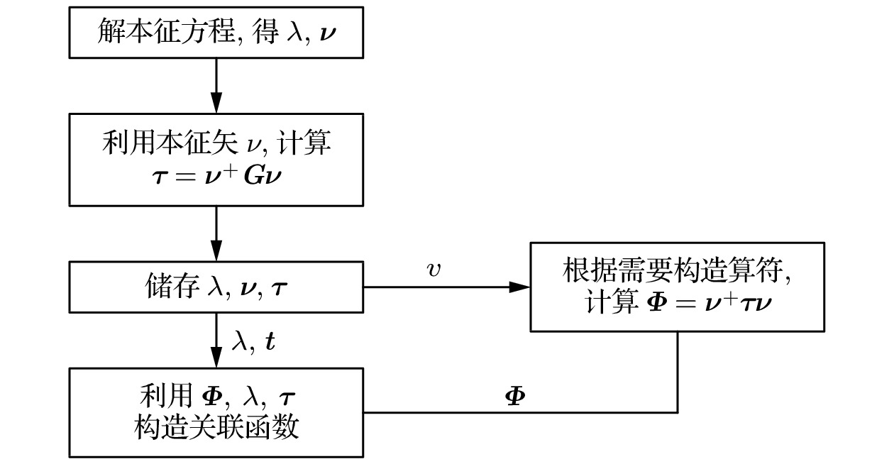
Lattice quantum chromodynamics (lattice QCD) is a theory based on quantum chromodynamics, which is widely used in strong interaction related calculations. As a research method that can give accurate and reliable theoretical results, with the improvement of computer ability, Lattice QCD is playing an increasingly important role in recent years. Distillation method is an important numerical method to calculate hadron correlation function in lattice QCD, and can improve the signal-to-noise ratio of calculated physical quantities. Distillation is a method to approximately compute full propagator via replace the laplacian operator with it's outerproduct of laplace eigenvectors. In this way, the construction of operators is independent of the inversion of propagator which is costful. The eigenvector system and perambulator can be used in different physical projects and we don't need to compute these data repeatedly. It's also convinent for computing disconnected part of correlation function. However, it also faces to the problem of large amount of data in constructing correlation function because the difficulty of compuation is proportional to the cubic of the number of eigenvectors, so it is necessary to further improve its computational efficiency. A program is developed in this work to construct correlation function of quark bilinear with distillation method, and solved the bottleneck of computing performance by using MPI(Message Passing Interface, https://www.open-mpi.org), OpenMP(Open Multi-Processing) and SIMD(Single Instruction Multiple Data) multi-level optimization technology. And this program distribute timeslices to different MPI processes because the computation of each timeslice is independent. In order to show the efficiency of our program some tests result are presented. After various tests of the program, it shows that our design can support large-scale computation. Under the strong scalability test, the parallel computing efficiency of 512 processes can still achieve about 70%. The ability of calculating correlation function is greatly improved. The correction of results also has been checked via compute pseudo-scalar correlators of charmonium. Three different $ 0^{-+}$ operators were adopted for variational analysis and there effecitive mass plateau were compared with the effective mass obtained from the tradional method with point source. The results of distillation method are consistent with traditional method. After variational analysis, three state is obtained, which means the variational analysis take effects and the correlation functions obtained from distillation method is reasonable.
NUCLEAR PHYSICS

2021, 70 (16): 162401.
doi: 10.7498/aps.70.20210503
Abstract +
Using the Monte Carlo method, the energy losses in silicon carbide of heavy ions with different linear energy transfers (LETs) are simulated and calculated. The simulation results show that the energy loss per unit depth of heavy ions in silicon carbide is affected by both the ion energy and the incident depth. Primary heavy ions and secondary electrons mainly cause energy loss, and the non-ionization energy loss only accounts for about 1% of the total energy loss. With the increase of LET, the initial angle and energy distribution of the secondary electrons become more and more concentrated. The peak position of the generated charge deposition is in the center of the heavy-ion track, and the distribution is linearly decreasing in Gaussian form in the direction perpendicular to the incident depth. In the californium source experiment of SiC MOSFET, when the drain voltage is 480 V, the device has a single event burnout, and the breakdown voltage of SiC MOSFET is less than 1 V after burnout has occurred. With the experimental results, we carry out the TCAD simulation of SiC MOSFET and obtain the electric field distribution inside the device under different drain voltages. The electric field parameters are used in the Monte Carlo simulation of SiC MOSFET with considering the metal layer. It is found in the Monte Carlo simulation that the greater the electric field of the epitaxial layer, the longer the path of heavy ions moving on the epitaxial layer is and the more the deposited energy, and that the secondary electrons are more likely to move in the direction of the electric field as the electric field increases, resulting in excessive energy deposition in local areas.
ATOMIC AND MOLECULAR PHYSICS
2021, 70 (16): 163101.
doi: 10.7498/aps.70.20202039
Abstract +
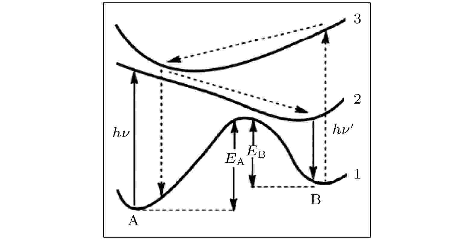
The photochromic switching mechanism of 2,3-difurylmaleic anhydride (DFMA) is investigated by first-principles calculations. Based on the stable structures of the open-ring (O-DFMA) and closed-ring (C-DFMA) of the DFMA, the minimum energy path (MEP) and the configuration of transition states (TS-DFMA) between the O-DFMA and C-DFMA are found by using the nudged elastic band (NEB) method, the potential barriers of O-DFMA and C-DFMA are 24959 cm–1(3.0945 eV) and 23328 cm–1(2.8923 eV), respectively, indicating that the DFMA molecule may be a thermally bistable molecule. Along the molecular configuration corresponding to the MEP curve (i.e. ground state S0), the potential energy curves of the lowest 8 singlet excited states of DFMA are calculated. Among these energy curves, only the first electronic excited state (i.e. S1 state) has a minimum value in the transition state (TS-DFMA) configuration. Combined with the molecular orbital transitions and orbital images, the photochromic mechanism of DFMA can be described as follows (1) From C-DFMA to O-DFMA process: under the action of the laser with S1–S0 resonance transition wavelength, the C-DFMA transits from S0 to S1 state, and then deactivates along the S1 potential energy curve, until a cross jumping transition occurs at the TS-DFMA structure from S1 to S0 and finally the molecule along the S0 potentioal energy curve returns to the O-DFMA configuration, then the switching action from closed-ring to open-ring is completed. The S1 state potential energy curve drops monotonically in this switching process, implying that there will be no fluorescent radiation in this process. (2) From O-DFMA to C-DFMA process: under the action of the laser with S1–S0 resonance transition wavelength, O-DFMA transits from S0 to S1 state. From the O-DFMA to TS-DFMA structure, there is a relatively “flat” area in the potential energy curve of the S1 state, and it decreases significantly only when it is close to the TS-DFMA. This means that O-DFMA needs to be excited with some vibrational modes to pass through the “flat” region of S1 and approaching to the TS-DFMA configuration, and then DFMA de-excites from the S1 state potential energy curve along a monotonic decline and a cross jumping transition from S1 to S0 occurs in the TS-DFMA configuration, completing the switching action from open-ring to closed-ring. It is also precisely because of the flat region of the potential energy curve of the initial S1 state that this excitation and switching process is accompanied by fluorescent radiations. The photochromic mechanism of DFMA indicates that it is suitable for making fluorescent molecular switches.

EDITOR'S SUGGESTION
2021, 70 (16): 163201.
doi: 10.7498/aps.70.20210193
Abstract +

EDITOR'S SUGGESTION
2021, 70 (16): 163202.
doi: 10.7498/aps.70.20210405
Abstract +
Coherent population oscillations spectroscopy, which is based on the interaction between atoms and the phase locked laser, is a kind of atomic population modulation spectroscopy. When the laser frequency difference is less than natural width of energy level, the coherent oscillation of atomic population will be induced by laser intensity modulation so that the probe laser transmission with narrow bandwidth can be realized. For a closed two-level system (TLS), the spectral line-width is limited mainly by the spontaneous emission lifetime of the upper atomic energy level. As for a three-level atomic system of Λ configuration, the two linearly polarized beams with both σ+ and σ- polarization component, the laser-atom interaction satisfies the selection rule. The spectral line-width mainly depends on the ground-state relaxation time, and the dependence on the line-width of spontaneous radiation is eliminated. In this paper, the laser from a external-cavity diode laser has its frequency locked to Cesium $6{{\rm{S}}_{1/2}}\left( {F = 3} \right) \to 6{{\rm{P}}_{3/2}}\left( {F' = 3} \right)$ transition. The frequencies of the two beams are shifted down by two independent double-passed acousto-optic modulators (AOM) to nearly resonate to Cesium $6{{\rm{S}}_{1/2}}\left( {F = 3} \right) \to 6{{\rm{P}}_{3/2}}\left( {F' = 2} \right)$ transition. The probe beam and the coupling beam are superposed at polarization beam splitter (PBS) cube and transmitted through the magnetically shielded cesium vapor cell in the same direction. The two beams have approximately the same Gaussian diameter of 6.6 mm. The beams are separated by another PBS behind the vapor cell, and the probe beam is detected by a photodiode. We realize the coherent population oscillation spectroscopy through the Cesium vapor cell at room temperature without buffer gas. The spectral linewidth is typically less than 50 kHz which is far below the spontaneous radiation linewidth(~5.2 MHz). The linewidth of coherent population oscillation spectroscopy of the Λ-type atomic energy level structure depends only on the population associated with the oscillation of multiple degenerate level systems except phase correlations of atomic states. Coherent population oscillation is beneficial to the obtaining of the narrow linewidth spectroscopy through the Rydberg atomic system with long excited state lifetime. Considering the importance of electric field measurement using Rydberg atoms, the method of coherent population oscillation can be used to improve the sensitivity of precise measurements based on Rydberg atoms.
EDITOR'S SUGGESTION
2021, 70 (16): 163301.
doi: 10.7498/aps.70.20210100
Abstract +
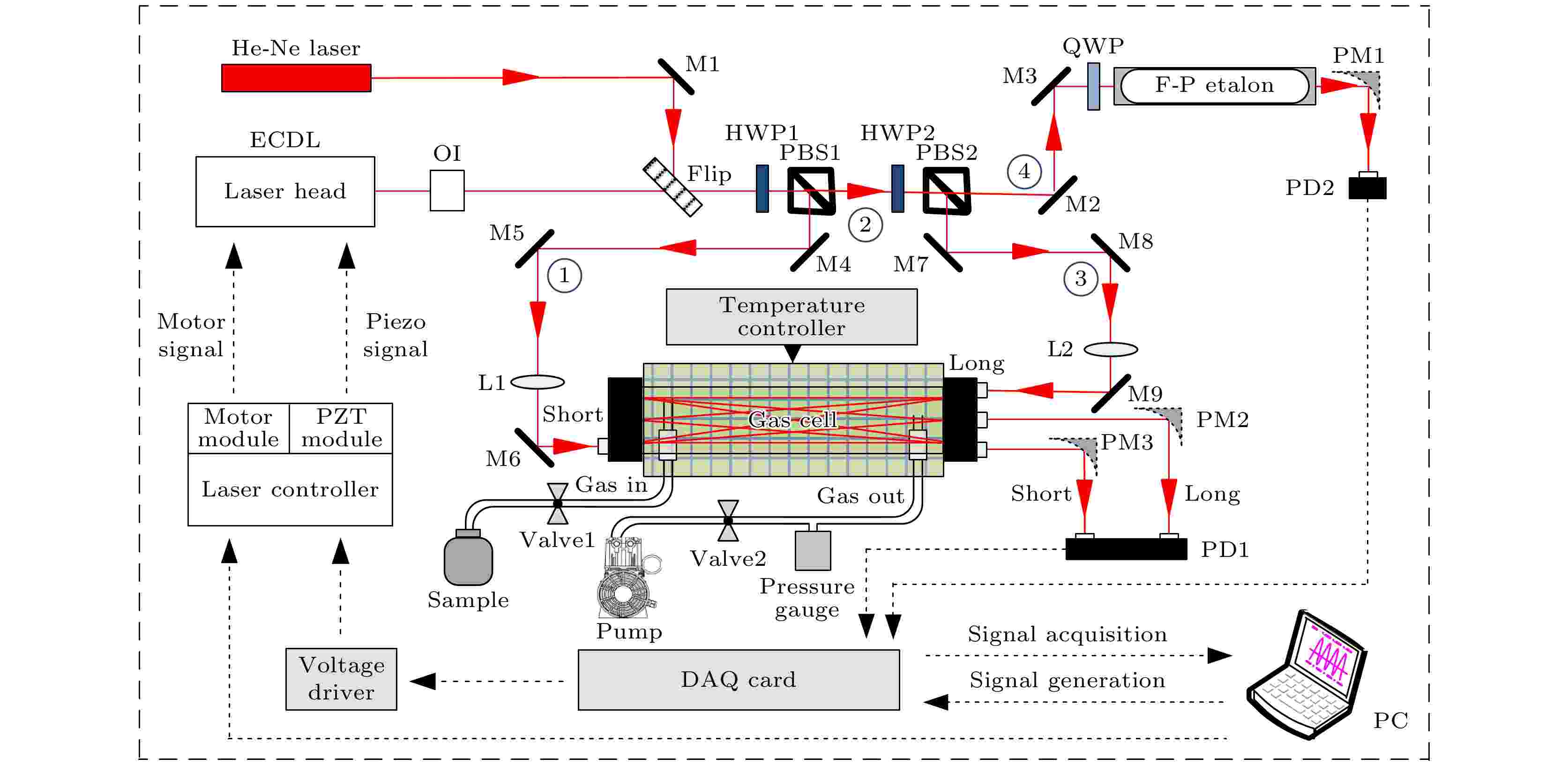
Based on the gas multi-pass absorption cell with dual-optical paths (long optical path: 72.46 m; short optical path: 36.23 m), a measurement method of simultaneously detecting water vapor absorption spectra is advanced. Combining with a narrow line-width external cavity diode laser and a high-precision Fabry-Perot etalon, a high-resolution simultaneous measurement device with dual-optical paths for water vapor absorption spectra in 1 μm band is developed. Since the external cavity diode laser has excellent polarization characteristics which could be combined with a half-wave plate and a polarization beam splitter to implement the laser transmissions in dual-optical paths simultaneously. Both the multi-pass absorption cell and the Fabry-Perot etalon in the measurement device have pressure and temperature control units, which are utilized for achieving ambient stability. The free spectral range of Fabry-Perot etalon is accurately measured by the method of optical comb frequency. Corresponding free spectral range with a deviation of only 0.02 % from the theoretical value is obtained to be a value of 749.52 MHz, and the influence of temperature on the frequency shift of etalon is less than 1 % of the measured value. The stability of the pressure and the temperature in the dual-optical path gas multi-pass absorption cell in the system are evaluated in detail, and the calculated relative errors are not more than 0.03 % and 0.02 %, respectively. At a temperature of 300 K, the system is used to measure the absorption spectra of water vapor at 9152.53 cm–1 from 400 Pa to 2000 Pa on dual-optical paths, then the integrated absorbance and Lorentzian line-width of water vapor for long optical path and short optical path are inverted by fitting absorption spectra with Voigt profile respectively. The absorption line intensities and self-broadening coefficients are acquired by performing linear fitting to the integrated absorbance and Lorentzian line-width under different pressures. And the relative deviations of the average values of the dual-optical path absorption line intensities (converted to the reference temperature of 296 K) and the self-broadening coefficients and the corresponding data of the HITRAN2016 database are 0.78 % and 3.8 %, respectively. Consequently, the feasibility of the dual-optical path simultaneous measurement method and the reliability of the measurement device are demonstrated by the results.
EDITOR'S SUGGESTION
2021, 70 (16): 163302.
doi: 10.7498/aps.70.20210522
Abstract +
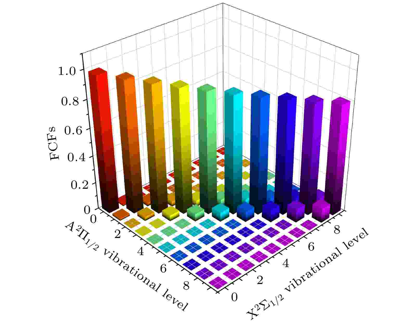
Laser cooling and trapping of neutral molecules has made substantial progress in the past few years. On one hand, molecules have more complex energy level structures than atoms, thus bringing great challenges to direct laser cooling and trapping; on the other hand, cold molecules show great advantages in cold molecular collisions and cold chemistry, as well as the applications in many-body interactions and fundamental physics such as searching for fundamental symmetry violations. In recent years, polar diatomic molecules such as SrF, YO, and CaF have been demonstrated experimentally in direct laser cooling techniques and magneto-optic traps (MOTs), all of which require a comprehensive understanding of their molecular internal level structures. Other suitable candidates have also been proposed, such as YbF, MgF, BaF, HgF or even SrOH and YbOH, some of which are already found to play important roles in searching for variations of fundamental constants and the measurement of the electron’s Electric Dipole Moment (eEDM). As early as 2004, the CaH molecule was selected as a good candidate for laser cooling and magneto-optical trapping. In this article, we first theoretically investigate the Franck−Condon factors of CaH in the ${{\rm{A}}}^{2}\Pi _{1/2}\leftarrow {{\rm{X}}}^{2}\Sigma _{1/2}$ transition by the Morse potential method, the closed-form approximation method and the Rydberg-Klein-Rees method separately, and prove that Franck−Condon factor matrix between $ {\mathrm{X}}^{2}\Sigma _{1/2} $ state and $ {\mathrm{A}}^{2}\Pi _{1/2} $ state is highly diagonalized, and indicate that sum of f00, f01 and f02 for each molecule is greater than 0.9999 and almost 1 × 10⁴ photons can be scattered to slow the molecules with merely three lasers. The molecular hyperfine structures of $ {X}^{2}\Sigma _{1/2} $ , as well as the transitions and associated hyperfine branching ratios in the ${{\rm{A}}}^{2}\Pi _{1/2}\left(J=1/2, \mathrm{ }+\right)\leftarrow {{\rm{X}}}^{2}\Sigma _{1/2}\left(N=1, \mathrm{ }-\right)$ transition of CaH, are examined via the effective Hamiltonian approach. According to these results, in order to fully cover the hyperfine manifold originating from $ |X, \mathrm{ }N=1, -\rangle $ , we propose the sideband modulation scheme that at least two electro-optic modulators (EOMs) should be required for CaH when detuning within 3Γ of the respective hyperfine transition. In the end, we analyze the Zeeman structures and magnetic g factors with and without J mixing of the $ |X, \mathrm{ }N=1, -\rangle $ state to undercover more information about the magneto-optical trapping. Our work here not only demonstrates the feasibility of laser cooling and trapping of CaH, but also illuminates the studies related to spectral analysis in astrophysics, ultracold molecular collisions and fundamental physics such as exploring the fundamental symmetry violations.
2021, 70 (16): 163303.
doi: 10.7498/aps.70.20202044
Abstract +
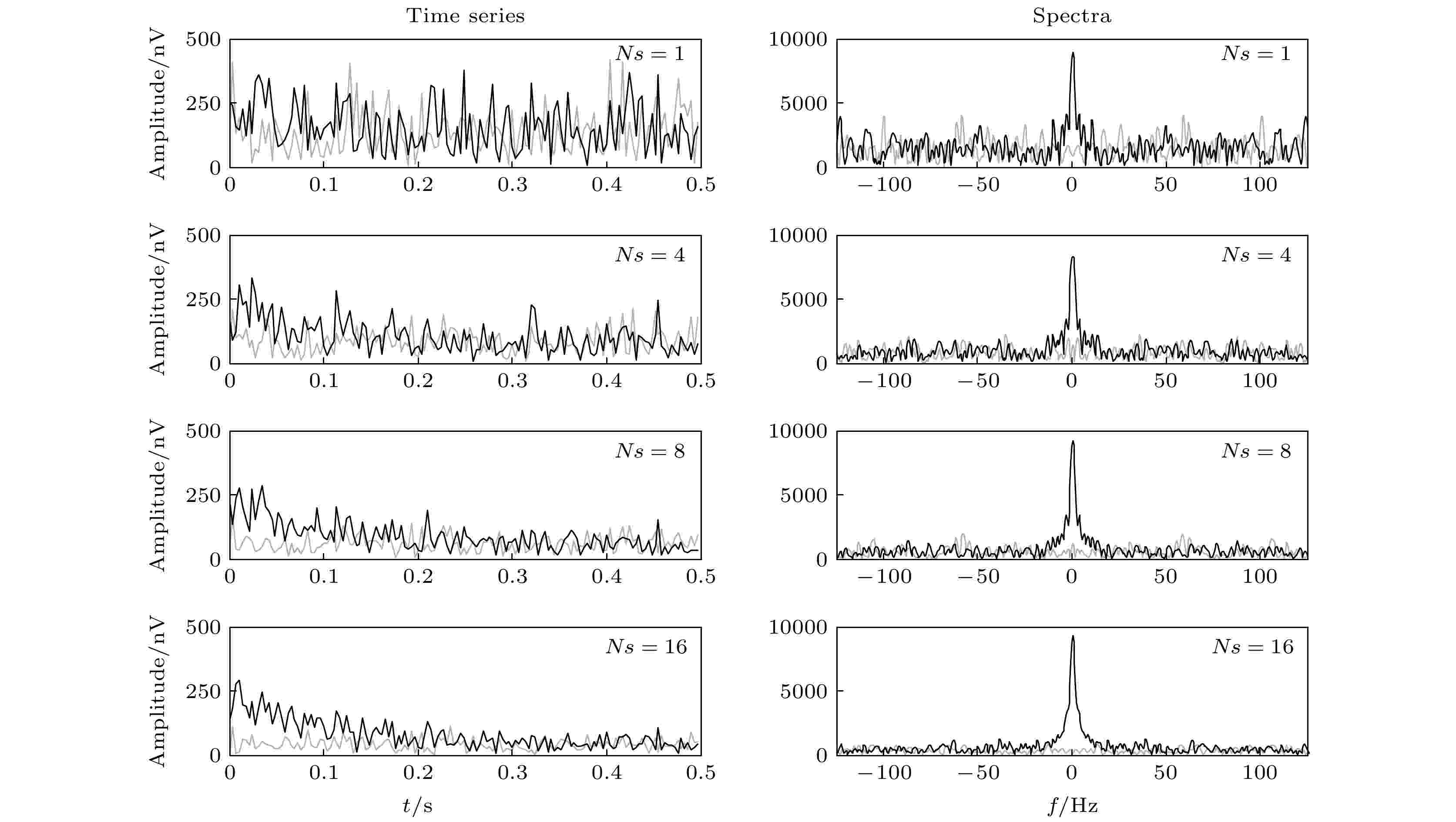
Magnetic resonance sounding (MRS) has the advantage of detecting groundwater content directly without drilling, but the signal-to-noise ratio (SNR) is extremely low which limits the application of the method. Most of the current researches focus on eliminating spikes and powerline harmonic noise in the MRS signal, whereas the influence of random noise cannot be ignored even though it is difficult to suppress due to the irregularity. The common method to eliminate MRS random noise is stacking which requires extensive measurement repetition at the cost of detection efficiency, and it is insufficient when employed in a high-level noise surrounding. To solve this problem, we propose a modified short-time Fourier transform(MSTFT) method, in which used is the short-time Fourier transform on the analytical signal instead of the real-valued signal to obtain the high-precision time-frequency distribution of MRS signal, followed by extracting the time-frequency domain peak amplitude and peak phase to reconstruct the signal and suppress the random noise. The performance of the proposed method is tested on synthetic envelope signals and field data. The using of the MSTFT method to handle a single recording can suppress the random noise and extract MRS signals when SNR is more than –17.21 dB. Compared with the stacking method, the MSTFT achieves an 27.88dB increase of SNR and more accurate parameter estimation. The findings of this study lay a good foundation for obtaining exact groundwater distribution by utilizing magnetic resonance sounding.
ELECTROMAGNETISM, OPTICS, ACOUSTICS, HEAT TRANSFER, CLASSICAL MECHANICS, AND FLUID DYNAMICS
2021, 70 (16): 164101.
doi: 10.7498/aps.70.20210334
Abstract +
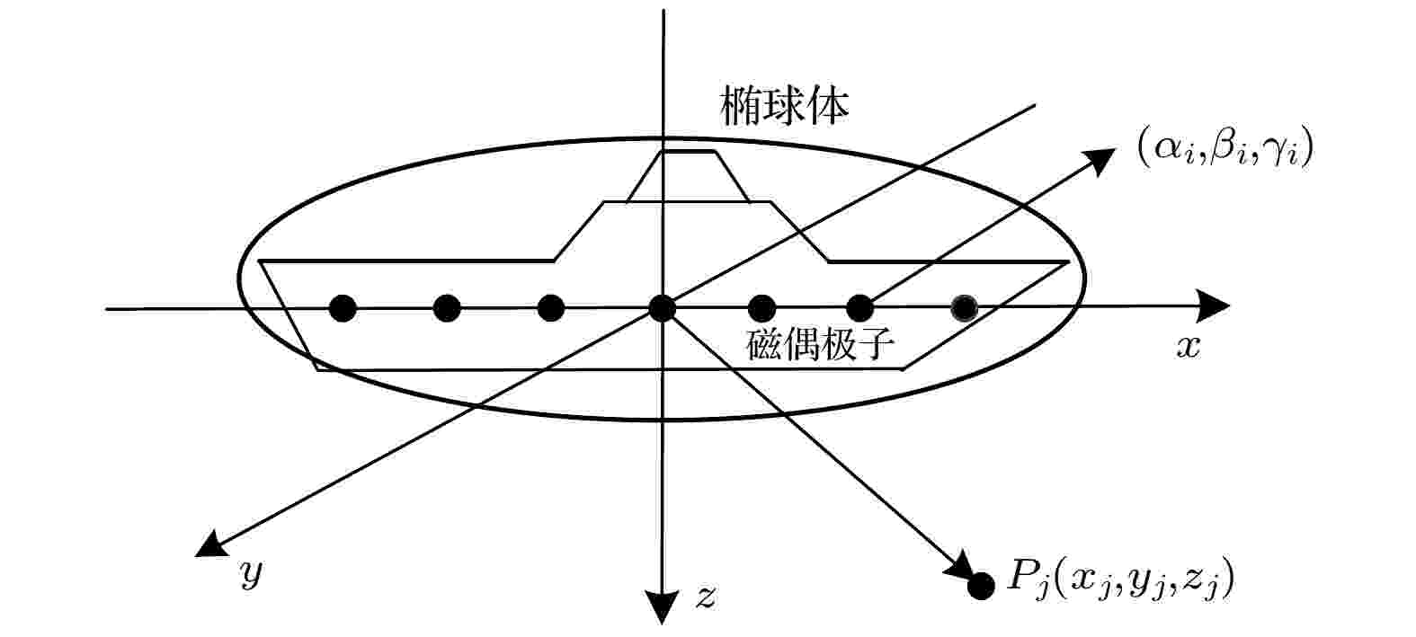
Ship magnetic field modeling is not only beneficial to understanding the characteristics of ship magnetic field, but also can predict the space distribution of ship magnetic field, which has an important application in ship protection and underwater weapons. Aiming at the problems of low modeling accuracy and poor stability in establishing the ship magnetic field hybrid model, a method of establishing a high precision stablity model is proposed in this paper. A hybrid model of magnetic field of a ship is established by using a uniformly magnetized rotating ellipsoid and a magnetic dipole array. Since the number and positions of magnetic dipoles in the hybrid model have an important effect on the modeling accuracy and stability, the fitting error function representing the modeling accuracy and the coefficient matrix condition number function representing the stability of the model are constructed by taking the magnetic dipole parameters as unknown variables. The multi-objective function is constructed by combining the fitting error function with the coefficient matrix conditional number function, which indirectly transforms the modeling problem into a multi-objective optimization problem. The multi-objective function is solved by using the multi-objective particle swarm optimization algorithm, and an optional set of modeling solution results is obtained. In order to select the best results from the optional set, the corresponding selection rules are designed based on the modeling accuracy. The proposed method is validated by the measured data of three kinds of ship models, the modeling results show that the relative error of the model is less than 3%, and the conversion error is less than 6%, which verifies that the proposed method can effectively model the ship magnetic field. Though the measurement data error exists, the modeling solution results from the proposed method have the best stability, which verifies that the modeling method proposed in this work has good stability. Compared with the two existing modeling methods, the proposed method has very good modeling accuracy and stability. Finally, the actual data of a ship on the sea are used for modeling, and the modeling results further verify that the proposed method has high modeling accuracy and conversion accuracy, and can be effectively applied to the relevant projects.
2021, 70 (16): 164201.
doi: 10.7498/aps.70.20210314
Abstract +
EDITOR'S SUGGESTION
2021, 70 (16): 164202.
doi: 10.7498/aps.70.20210287
Abstract +
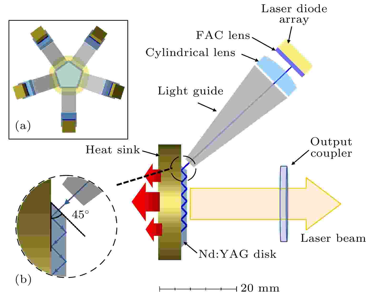
The high-average-power diode-pumped solid-state laser is one of the main research directions in the field of international laser technology, and has major applications in the fields like space exploration, precise detection, fusion research, etc. Under high-power pumping conditions, the conventional rods or slabs are not conducive to effectively removing waste heat. And the thermal effect causes the quality of the laser beam to deteriorate, which limits the further increase of the output power. In this article, the polygonal Nd: YAG thin disk is taken as a gain medium for the laser, and experiments verify that the side pumping method can obtain a higher output power of the all-solid-state pulsed laser while ensuring high beam quality. The gain medium is a regular pentagonal Nd: YAG thin disk with a side-cut-angle of 45°, the crystal thickness is 1.5 mm, and the diameter of the inscribed circle on the front face is 16 mm. Five laser diode arrays are placed symmetrically around the disk, and the pump surfaces are parallel to the sides of the disk. The pump laser propagates along the zigzag path between the upper and lower surface of the disk, thus improving the absorptive efficiency and pump uniformity. Through the optimization study of its gain characteristics and optical characteristics, the high-efficiency high-uniform pumping is achieved. Along the pump light coupling transmission path, the fast-axis collimator is used to control the beams in the fast-axis direction to be nearly parallel, and the large-area pump light is compressed through the coupling structure of cylindrical lens and light guide to match the size of the thin disk, and the pump coupling efficiency measured experimentally is 97%. When the Nd3+ doping concentration in the crystal is 0.3 at.%, the gain medium absorptive efficiency is 87%, and the root mea squared pump absorptive distribution uniformity in the gain medium is 3.21%. The fluorescence distribution of the gain medium is in good agreement with the simulated data. When the pump energy is 2.2 J, a laser output with an energy of 0.85 J is obtained, and optical-to-optical efficiency and slope efficiency are 38.8% and 40.1%, respectively. The single pulse energy stability is 2.7%(RMS) at 1 Hz frequency. In the stable cavity, the beam quality β - factor is measured to be about 10.
2021, 70 (16): 164203.
doi: 10.7498/aps.70.20210095
Abstract +
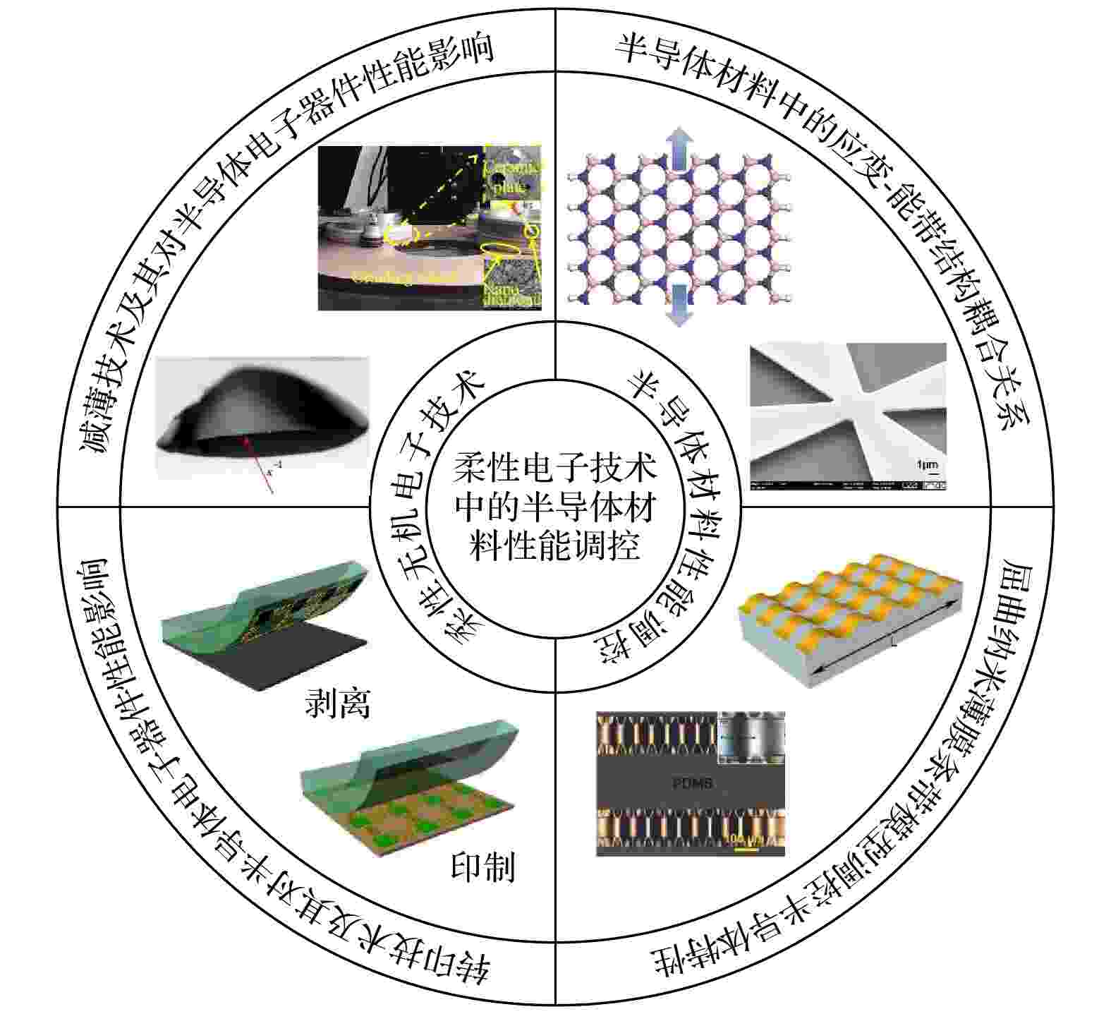
Flexible electronics technology plays an important role in regulating the properties of semiconducting materials, leading to the breakthrough in traditional strain engineering that is limited by the rigid and brittle inorganic materials and the fixed strain values. Thereby, the relevant research not only provides a new clue for strain regulation of semiconductor materials or other functional materials, but also lays a theoretical foundation for the performance evaluation of stretchable and flexible electronic devices based on inorganic functional materials in large-deformation environments. In this paper, the research progress of flexible inorganic electronics and strain effects on band structures, especially the property regulation of semiconducting materials in flexible electronics, is reviewed. Firstly, the nano-diamond particles based thinning process and the transfer printing are emphatically expounded with their influence on the properties of semiconducting electronics explored. In addition, the development and application of strain effect on band structure in recent years are introduced. In particular, the strain control based on buckling GaAs nanoribbon and buckling quantum well structure are studied to demonstrate the superior advantage of flexible electronics technology in the property regulation of semiconducting materials. The application and developing trend of strain engineering in the future are prospected finally.
PHYSICS OF GASES, PLASMAS, AND ELECTRIC DISCHARGES
2021, 70 (16): 165201.
doi: 10.7498/aps.70.20210461
Abstract +
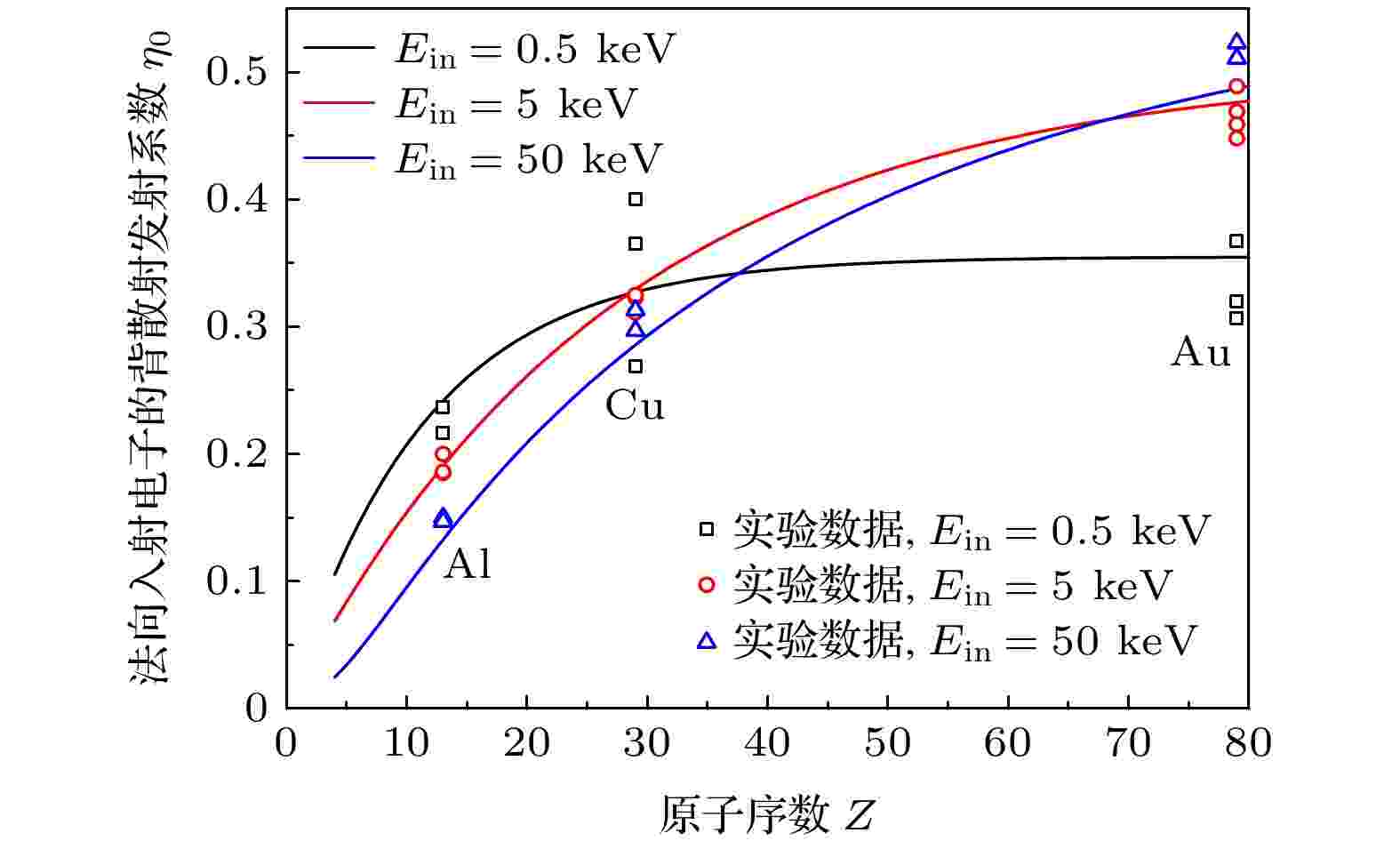
It is difficult to effectively shield the system generated electromagnetic pulse (SGEMP), which can significantly affect the performance of important electronic devices and infrastructure, such as low-orbit spacecraft. Numerical simulation is an essential way to study the SGEMP response. However, many previous studies ignored or simplified the effect of secondary electron emission in their models. In this paper, a three-dimensional electromagnetic particle-in-cell numerical simulation model is developed to evaluate the effect of secondary electrons on the SGEMP response of two typical structures (external SGEMP and cavity SGEMP, respectively) under different current densities (0.1–100 A/cm2) and different materials (Al, Cu and Au). A right cylinder or cylindrical cavity with a length of 100 mm is used. The photoelectrons produced by the interaction between the X-ray photon and metal are emitted from one end of the system and assumed to be monoenergetic. The photoelectron pulse follows a sine-squared distribution, and its full width at half maximum is 1 ns. Some important parameters of secondary electrons are discussed and summarized, including the emission coefficients of elastically and inelastically backscattered electrons, as well as the probability density functions of emission angles and energies. The results show that ignoring the secondary emission in the simulation model leads the peak electric field to be underestimated by twice-thrice, and the duration of electric field response by more than 10%. The oscillation frequency and the amplitude of the second peak of the tangential magnetic field are also increased, with the secondary electrons considered. Among various types of secondary electrons, backscattered electrons have a dominant effect on the change of SGEMP. The effect of true secondary electrons is about 1/5 of that of backscattered electrons. The effect of secondary electrons on SGEMP response increases with a higher atomic number of the material used in the system, mainly due to higher backscattering emission coefficient and a high ratio of high energy inelastically backscattered electrons. The secondary electrons will influence the response of the external SGEMP only when the space charge effect is strong (high X-ray fluence). While the response of the cavity SGEMP is more easily affected by the secondary electrons even at a relatively low X-ray fluence. This paper helps to better obtain the SGEMP response of a specific device under strong radiation through numerical simulation.
2021, 70 (16): 165202.
doi: 10.7498/aps.70.20210441
Abstract +
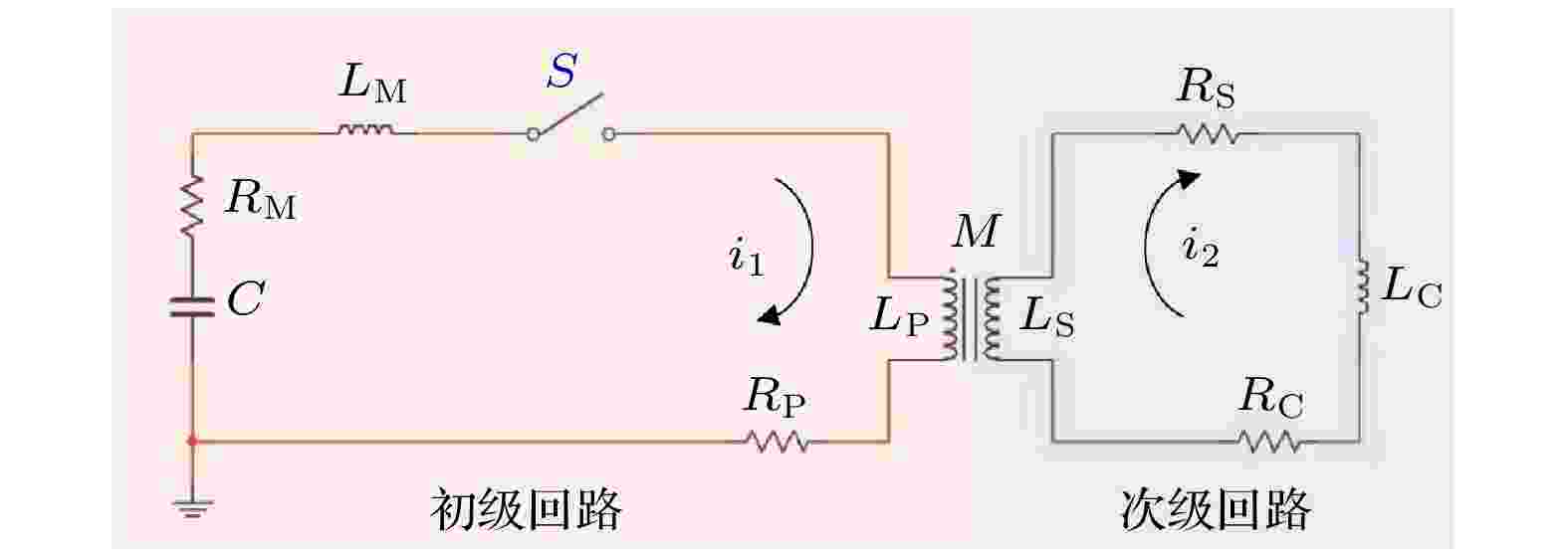
Magnetized laser plasma has attracted a lot of attention in recent years especially in magnetized inertial confinement fusion, laboratory astrophysics, and industrial application. Pulsed intense magnetic field device is the core equipment of magnetized laser plasma experiment. Here in this work, an inductively coupled coil is developed to optimize the pulsed intense magnetic field device. The primary coil of a multi-turn solenoid is used instead of a single-turn coil. Then the energy of the solenoid is delivered to the secondary coil via inductively coupled transformer, which increases the current density markedly. The current generates a stronger magnetic field in the single-turn magnetic field coil. The influence of the diameter and the number of turns of the primary solenoid of the inductively coupled coil on the magnetic field are explored in experiment and simulation. It is found that for a discharge system of 2.4 μF capacitance, the optimized parameters of the primary solenoid are 35 turns and 35 mm diameter. The optimized magnetic field is 3.6 times stronger than that of the conventional directly connected single-turn coil. At a charging voltage of 20 kV, the peak magnetic field reaches 19 T in a magnetic field coil of 5 mm inner diameter. The inductively coupled coil made of CuBe solves the problem of coil expansion in intense magnetic field, and a peak magnetic field of 33 T is obtained at a charging voltage of 35 kV. The present approach creates stronger magnetic field environments. At the same time, the inductively coupled coil reduces the requirements for system inductance, so that components such as energy storage capacitors and switch can be placed far from the coil, which improves the flexibility of the experiment setup.
CONDENSED MATTER: STRUCTURAL, MECHANICAL, AND THERMAL PROPERTIES
2021, 70 (16): 166101.
doi: 10.7498/aps.70.20210515
Abstract +
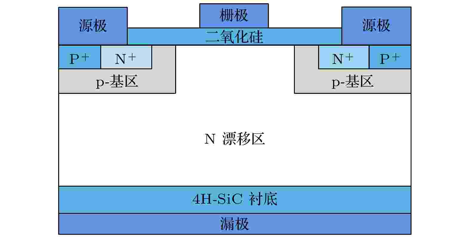
In this paper, silicon carbide field effect transistor device is taken as a research object, and the cobalt source irradiation experiment is conducted under different voltages and different temperatures and the annealing experiment is also performed after irradiation. The semiconductor parameter analyzer is used to test the direct current (DC) parameters of the device, and the changes in the radiation sensitive parameters of the device in the irradiation and annealing process are studied. The reasons for the influence of voltage and temperature on the radiation degradation of the device are analyzed, and the annealing recovery is also explored. The results show that the oxide trapped charge induced by irradiation is the main reason for the degradation of the electrical parameters of the silicon carbide field effect transistor device. The voltage and temperature can affect the final yield of the oxide trapped charge, which causes the device to produce the difference in the degree of degradation after irradiation at different voltages and different temperatures; in the annealing process, due to the annealing of the tunneling of oxide trapped charges, the electrical performance of the device can be restored partially.
EDITOR'S SUGGESTION
2021, 70 (16): 166201.
doi: 10.7498/aps.70.20210089
Abstract +
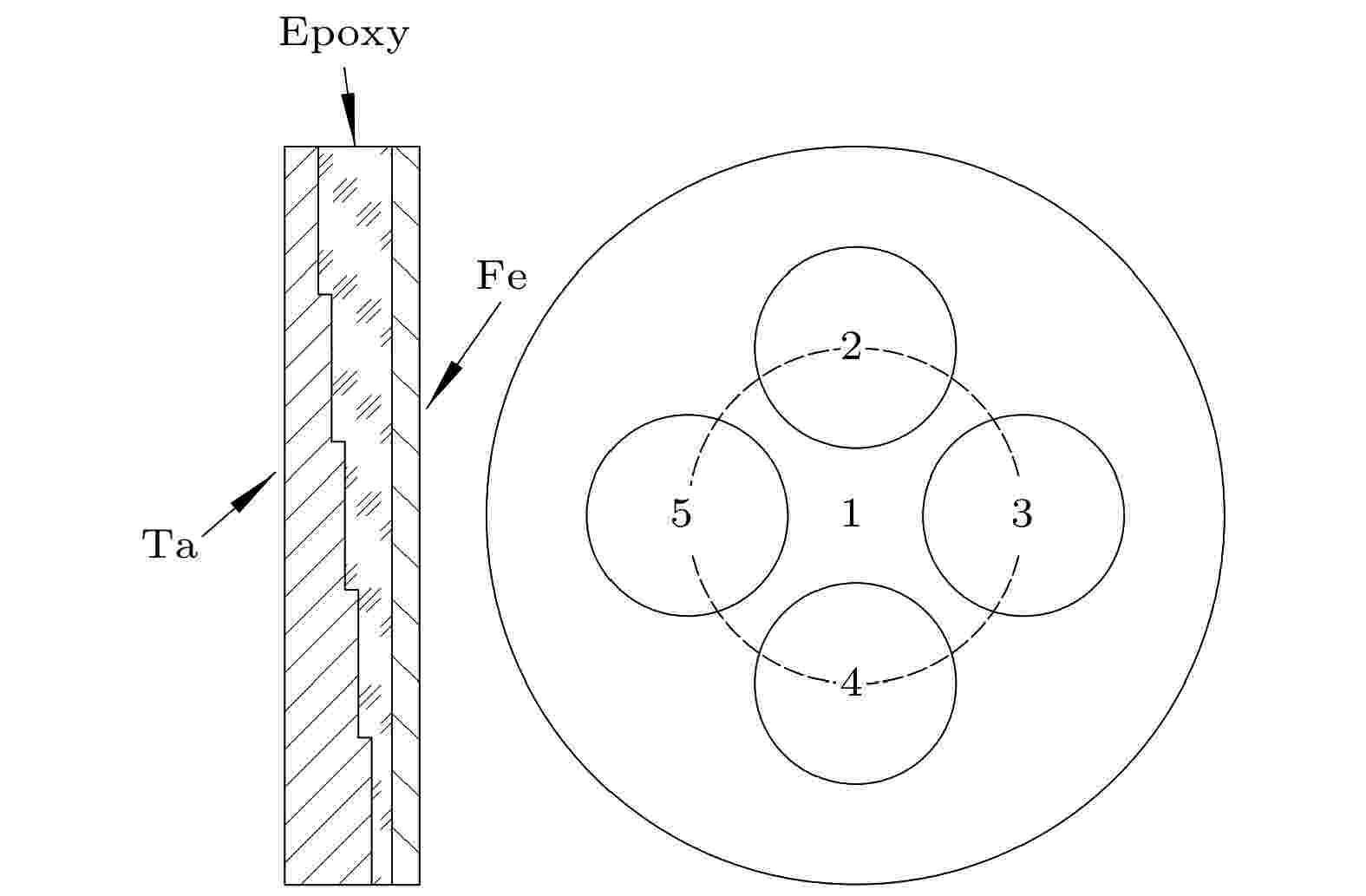
The dynamics of iron under extreme conditions like high temperature and high pressure has been well studied for several decades. But, there have been not many reports about the phase transition kinetics coupled with complicated thermodynamic paths, especially loading-unloading-reloading path, which is closer to the real applications. A three-layer structure impactor with five stages performed in the front-surface experiment is made up to approach the special path. We choose epoxy to be the adhesive as it has low impedance and high strength. Tantalum, the standard material of high impedance which also has single wave structure, is selected for reloading process. The wave profile shows a 3-wave structure in the first unloading period and the inverse phase transition threshold is calculated to be about 11.3 GPa. This onset pressure of reverse phase transition is not consistent with Barker’s result, higher than his result (about 2.5 GPa). By comparing with recalculated result of Jensen’s data, we find that our result is consistent with theirs.In this work the inverse phase transition ends at about 10 GPa, the value from this way which is higher than Barker’s finding, even higher than his result of the threshold pressure of reverse phase transition. And at this state there remains 12%–15% of ε phase. So it cannot be seen as the completed reverse phase transformation. The phase transition onset pressure is 10–12 GPa on the reloading path and it is about 1–2 GPa lower than the first phase transition. By simulating the wave profile, the discrepancy of using different phase transformation characteristic time τ as 30 ns and 5 ns is analyzed. It can be seen that the phase transition rate of reloading is faster than that of the first loading process. These phenomena may be caused by the twins and the dislocations which are produced by the inverse phase transition. Also, as unloading time becomes longer, the mass fraction of ε phase becomes lesser and the onset pressure of α → ε phase transition becomes lower. This because with more ε phases transforming into α phase, more twins and dislocations will be produced in material. Therefore, it brings the lower onset pressure.

2021, 70 (16): 166301.
doi: 10.7498/aps.70.20210271
Abstract +
Monolayer tellurene is a novel two-dimensional semiconductor with excellent intrinsic properties. It is helpful in understanding doping and scattering mechanism to study the electronic structure of defective tellurene, thus it is important for the application of tellurene in electronic and photo-electronic devices. Using first-principles calculation based on the density functional theory, we investigate the effects of commonly seen point defects on the electronic structure and optical properties of monolayer β-Te. Seven kinds of point defects that may be present in β-Te are designed according to the lattice symmetry, including two single vacancies (SV-1, SV-2), two double vacancies (DV-1, DV-2) and three Stone-Wales (SW) defects (SW-1, SW-2, SW-3). It is found that the defect formation energies of these defects are 0.83–2.06 eV, which are lower than that in graphene, silicene, phosphorene and arsenene, suggesting that they are easy to introduce into monolayer β-Te. The two most stable defects are SV-2 and SW-1 where no dangling bond emerges after optimization. The calculated band structures show that all seven defects have little effect on the band gap width of monolayer β-Te, but they can introduce different numbers of impurity energy levels into the forbidden band. Among them, the SV-1, SV-2, DV-1 and SW-2 each act as deep level impurities which can be recombination centers and scattering centers of carriers, SW-1 acts as a shallow level impurity, DV-2 and SW-3 act as both deep level impurity and shallow level impurity. Besides, SW-1, SW-2 and DV-1 can change the band gap of monolayer β-Te from direct band gap to indirect band gap, which may result in the increase of the lifetime of carriers and decrease of photoluminescence of monolayer β-Te. The optical properties of monolayer β-Te, which are sensitive to the change in band structure, are also affected by the presence of defects. New peaks are found in the complex dielectric function and the absorption coefficient of defective monolayer β-Te in an energy range of 0–3 eV, of which the number and the position are dependent on the type of defect. The SV-1, DV-1, DV-2 and SW-2 can enhance the light response, polarization ability and light absorption in the low energy region of monolayer β-Te. This research can provide useful guidance for the applications of β-Te in the electronic and optoelectronic devices.

2021, 70 (16): 166302.
doi: 10.7498/aps.70.20210268
Abstract +
CdS/CdMnTe heterojunction is the core of photoelectric conversion of CdMnTe film solar cells, whose interface properties have an important influence on the cell efficiency. In this study, the first-principles calculation method based on density functional theory is used to build the surface model for each of the CdS (002) and the CdMnTe (111) and the model of CdS/CdMnTe heterojunction with Mn atoms occupying different positions, and to analyze their electronic properties and optical properties. The results show that the lattice mismatch of the CdS/CdMnTe heterojunction is about 3.5%, the atomic positions and bond lengths of the interface change slightly after relaxation. The density of states shows that there is no interface state near the Fermi level in CdS/CdMnTe interface. Besides, the atoms at CdS/CdMnTe interface are hybridized, which can enhance the interface bonding. The differential charge density analyses indicate that the charge transfer mainly occurs at the interface, and electrons transfer from CdMnTe to CdS. The optical analysis shows that CdS/CdMnTe heterojunction mainly absorbs ultraviolet light, and the absorption coefficient can reach 105 cm–1. However, the optical properties of heterojunctions with different Mn atom positions are slightly different. In a range of 200–250 nm, the absorption coefficient of the heterojunction with Mn atom in the middle layer is larger, but in a range of 250–900 nm, the absorption peak of the heterojunction with Mn atom in the interface layer is higher. The results in this paper can provide some references for improving the photoelectric conversion efficiency of stacked solar cells through the reasonable construction of the heterojunction model and the analysis of the interface photoelectric performance, which is beneficial to the experimental research of multi-band gap heterojunction.
2021, 70 (16): 166401.
doi: 10.7498/aps.70.20210361
Abstract +
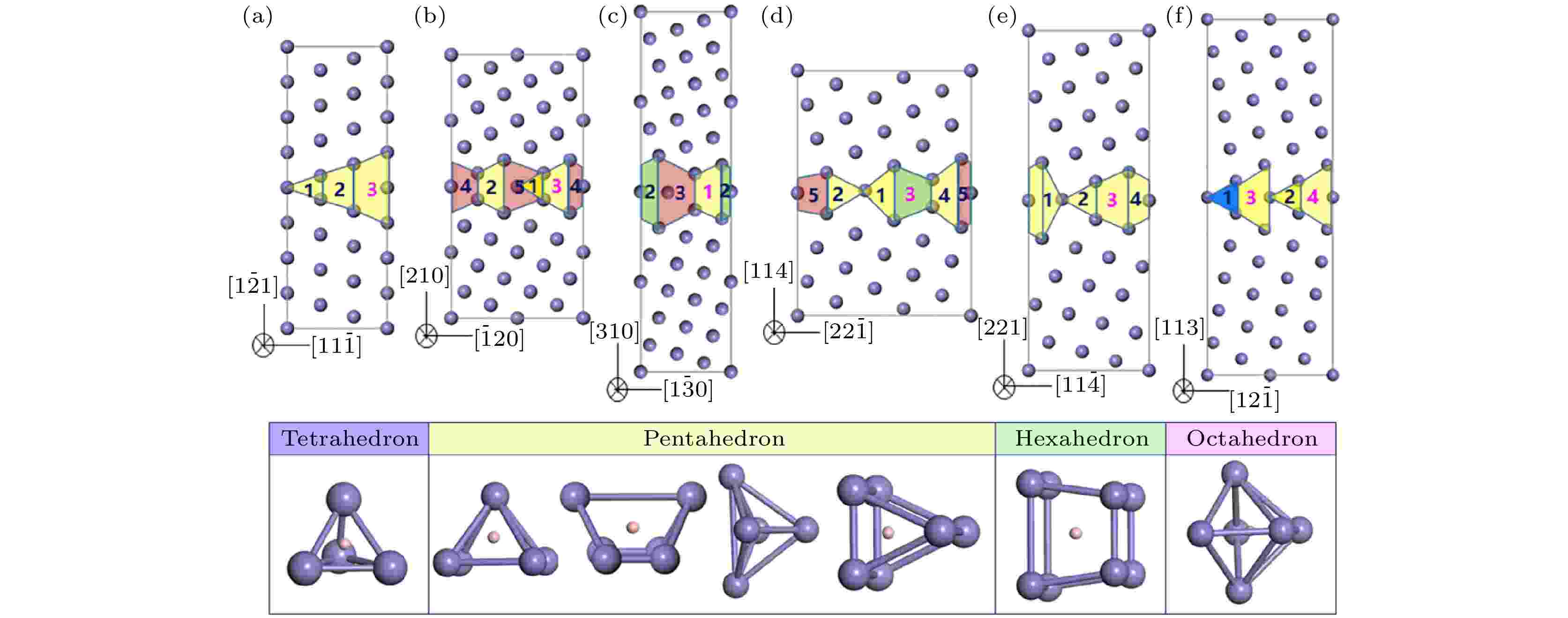
Boron, a commonly used microalloying element in steel, is distributed mainly at the grain boundary of stainless steel and plays an important role in regulating the mechanical, corrosion resistance and grain boundary structure of stainless steel. Owing to the small amount of boron added into the steel, it is difficult experimentally to detect the traces of boron segregation at the grain boundary, not to mention analyzing the structural characteristics of the boron segregation grain boundary. First-principles density functional theory (DFT) provides convenience in analyzing the existence mode and mechanism of boron in austenitic steel from the atomic level. Combining with the actual grain boundary structure types in austenitic stainless steel, Fcc-Fe Σ3(112), Σ5(210), Σ5(310), Σ9(114), Σ9(221) and Σ11(113) symmetric tilt grain boundaries are constructed based on DFT, and the segregation behaviors of boron atoms at the six grain boundaries are studied to reveal the segregation mechanism from the atomic and electronic level. The results show that boron segregation occurs mostly at Σ5(210), Σ5(310) and Σ9(114) grain boundaries, while a relatively weak segregation tendency is observed at Σ9(221), Σ3(112) and Σ11(113) grain boundaries; boron atom preferentially occupies the pentahedral or hexahedral segregation position with the largest coordination number; the interface adhesive strength at grain boundaries is improved by the segregation of boron according to the tensile test, which complies with the calculation results of Rice-Wang thermodynamic model; the chemical effect caused by the increase of local charge density after boron segregation at Σ9(114) grain boundary outstrips the adverse effect of structural changes, and the strong interaction between B-p electrons and Fe-s electrons improves the interface adhesive strength. The results provide a reference for using boron to optimize the interface structure of austenitic stainless-steel.

2021, 70 (16): 166801.
doi: 10.7498/aps.70.20210386
Abstract +
Hexagonal boron nitride (h-BN) has huge potential applications in micro-nano electromechanical system due to its good lubricity and insulation. In this paper, a microporous array is prepared on a SiO2/Si substrate by the substrate etching process, and then the h-BN is transferred to the microporous substrate to form a suspension structure. The effect of electric field on tribological properties of suspended h-BN is studied by atomic force microscopy. The results show that the friction of the suspended h-BN is smaller than the friction on the h-BN supported by the substrate, because the greater in-plane stretch weakens the puckering effect. The electric field increases the friction of the suspended h-BN, and the influence of positive bias is greater than that of negative bias. The application of the electric field increases the electrostatic force on the tip, thereby increasing the additional load and the interface barrier in the friction process. The electric field causes the stick-slip behavior to change from single-slip to multi-slip. Compared with the h-BN supported by the substrate, h-BN in the suspended state is strongly affected by the electric field. The reduction of the interface distance and the absence of the substrate oxide layer lead the electrostatic force to increase. This paper proposes a method to adjust h-BN’s friction by electric field, which provides theoretical guidance for studying the friction characteristics of two-dimensional materials.
2021, 70 (16): 166802.
doi: 10.7498/aps.70.20201594
Abstract +
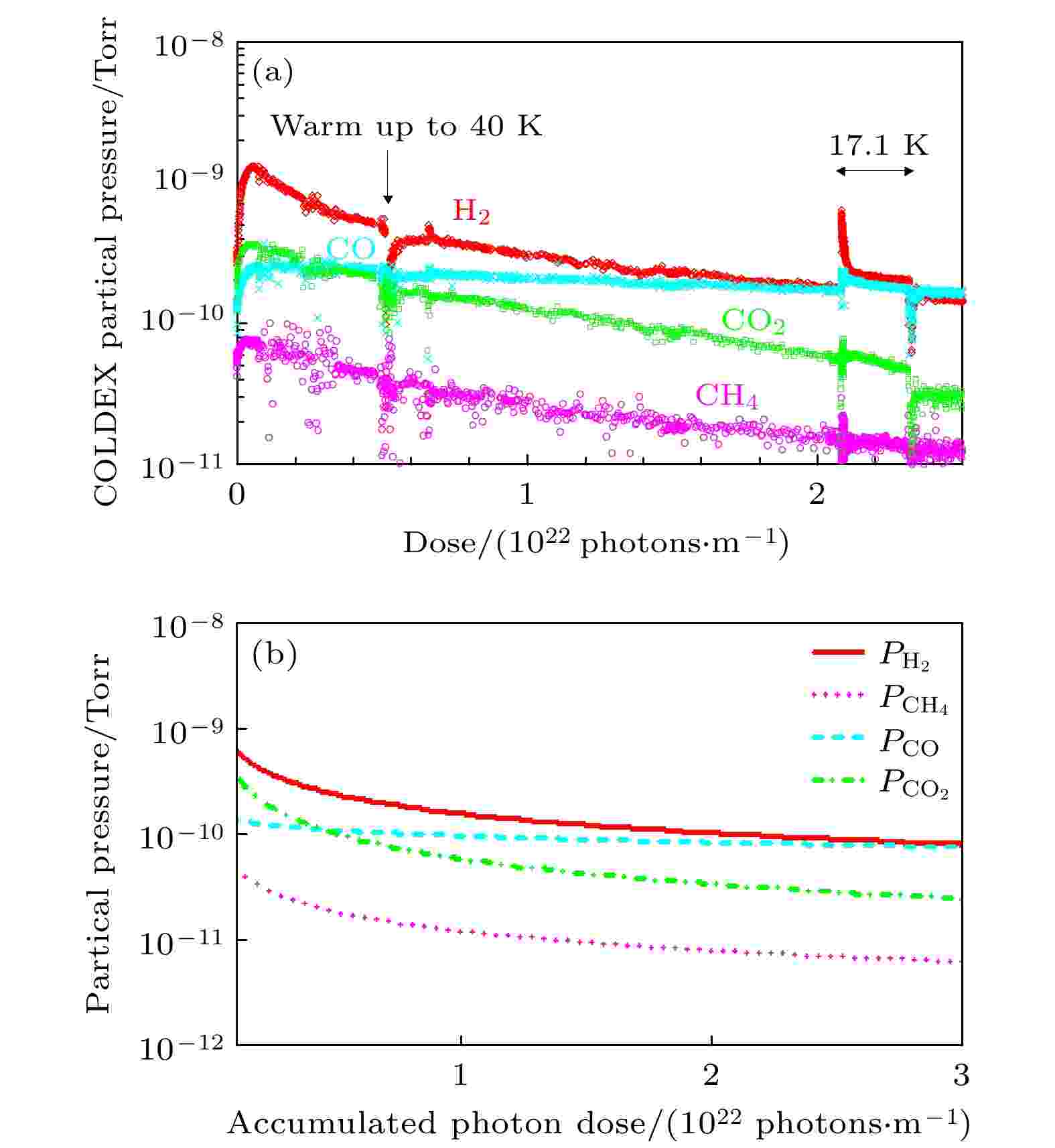
Vacuum stability is one of the key issues in the design of particle accelerators, especially high-energy super proton-proton colliders. The synchrotron radiation generated by proton beams in the bending area will desorb and crack the gas molecules which have adsorbed on the wall of the cold bore. The collision or scattering between the proton beam and the desorbed gas molecules may result in the degradation of the beam quality and the reduction of beam life time, and even the collapse of the beam. Usually a copper coated stainless steel beam screen is installed in the cold bore to intercept synchrotron radiation and reduce gas desorption. Based on the design parameters of the Super Proton-Proton Collider, in this paper the source of gas in the beam screen is analyzed. By considering the photon-induced desorption process and the gas molecule cracking process, the gas dynamic model in the beam screen is established. Moreover, the calculation of the evolution of the gas density in the beam screen with the beam operating time is carried out, and the effect of TiZrV non-evaporable getter film coated beam screen on the dynamic gas density is explored. The results show that H2 is the main desorption gas in the beam, the next is CO, while the molecular density of CO2 and CH4 are limited by molecular cracking. The maximum gas density in the beam screen appears at the initial stage of operation, and the gas density decreases with time going by. In order to strengthen adsorption and reduce desorption, TiZrV coated beam screen is discussed in this paper. In the case of TiZrV coated stainless steel beam screen, the maximum equivalent H2 density is about two order of magnitude lower than in the case of copper coated stainless steel beam screen. The non-evaporable getter(NEG) for beam screen material can significantly improve vacuum performance. The calculation results can qualitatively reflect the dynamic vacuum evolution in the beam screen during the beam operation and provide a reference for designing vacuum systems.
CONDENSED MATTER: ELECTRONIC STRUCTURE, ELECTRICAL, MAGNETIC, AND OPTICAL PROPERTIES
2021, 70 (16): 167101.
doi: 10.7498/aps.70.20210536
Abstract +
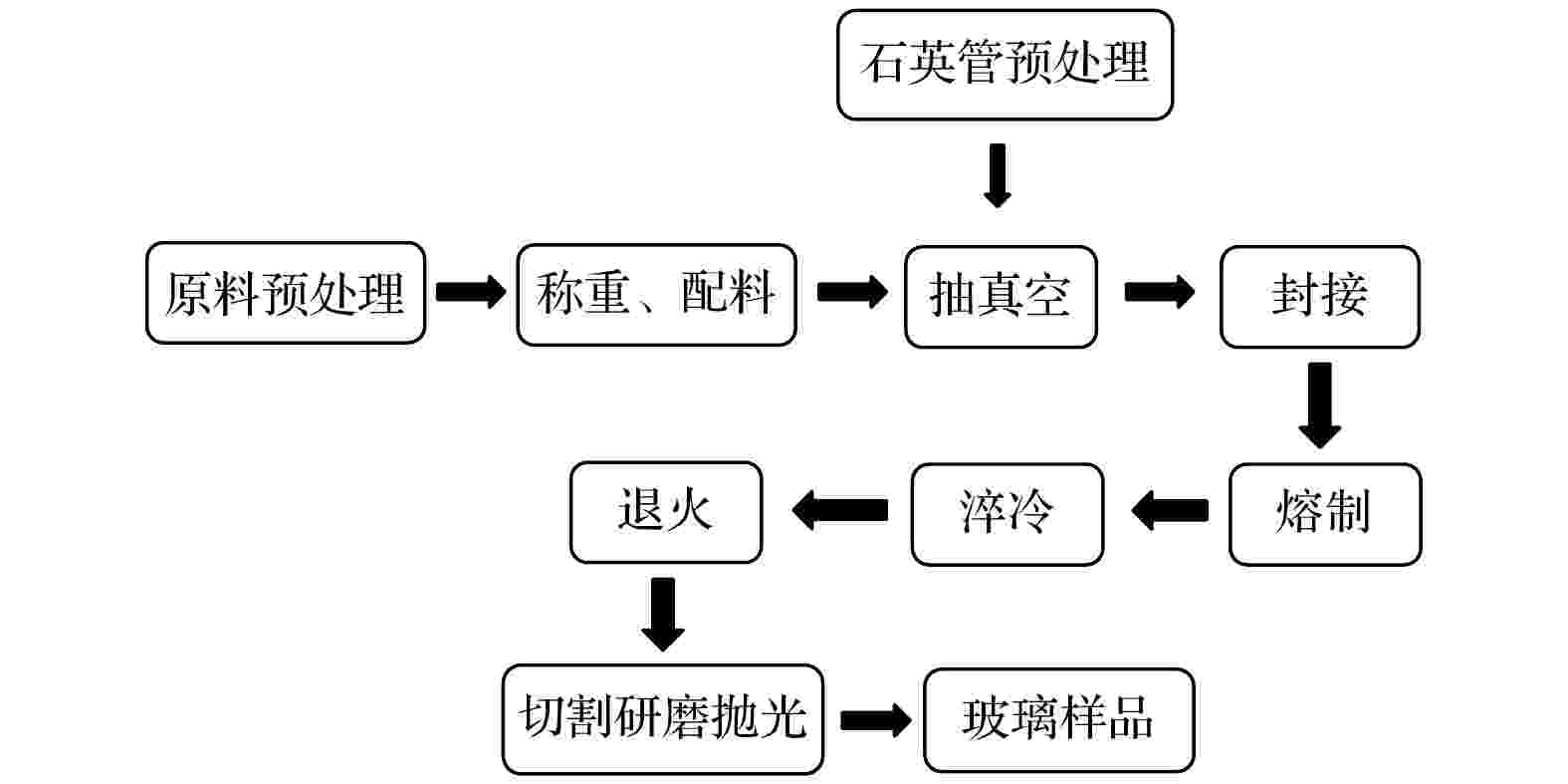
In this paper, chalcogenide glasses Ge11.5As24Se64.5–xSx (x = 0, 16.125%, 32.25%, 48.375% and 64.5%) are prepared and their optical properties are studied in order to select the best components for the use in optical devices. The values of laser damage threshold, refractive index, and third-order nonlinear refractive index, as well as the absorption spectra of the glasses are measured. The results show that the linear and third-order nonlinear refractive indices of the glass decrease gradually, the glass optical band gap increases gradually, and the laser damage threshold increases continuously after the high threshold component S atoms have been introduced gradually. We further investigate the structural origins of these changes in physical properties by Raman scattering spectra and high resolution X-ray photoelectron spectroscopy. By analyzing the evolution process of different structural units in the glass, it is found that the heteropolar bonds (Ge—Se/S, As—Se/S) are dominant in these glass network structures, and compared with Se, and that Ge and As prefer to bond with S. As the ratio of S/Se increases, the number of chemical bonds related to Se (Ge—Se, As—Se and Se—Se) decreases gradually, while the number of chemical bonds related to Se (Ge—S, As—S and S—S) increases gradually, which has little effect on the change of the topological structure of glass. It can be concluded that the main reason for the change of physical properties of glass is the difference of the strength between chemical bonds in the glass structural system.
2021, 70 (16): 167201.
doi: 10.7498/aps.70.20210454
Abstract +
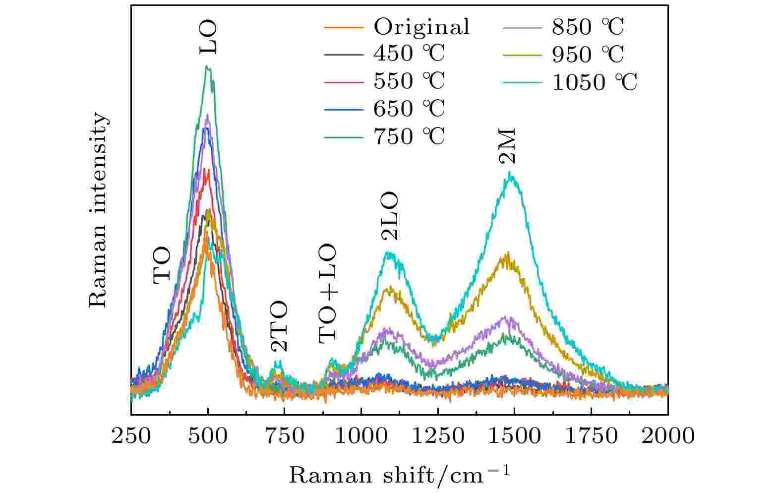
Laser Raman spectroscopy is used to study the enhancement effect of two-magnon scattering in nickel oxide through annealing treatment in a temperature range from 450 ℃ to 1050 ℃, and investigate laser heating effect on two-magnon scattering. Our study shows that two-magnon scattering of nickel oxide can be tremendously enhanced with annealing temperature rising. In the temperature range from 450 ℃ to 1050 ℃, the enhancement increases with annealing temperature increasing, and with 1050 ℃ annealing the two-magnon scattering can be enhanced more than two orders of magnitude, also the enhancement of two-magnon scattering is much stronger than that of two-phonon scattering. This tremendous enhancement is correlated not only with the significant decrease of Ni-vacancy by high temperature annealing, but also with the magnetic spin ordering network of Ni ions. The variation of sensitive intensity of two-magnon scattering with the concentration of Ni-vacancy can be used to provide a simple Raman spectroscopy method of quantitatively measuring the Ni-vacancy in nickel oxide. In addition, the annealing treatment can significantly reduce the laser heating effect on two-magnon scatting in nickel oxide power samples. At low annealing temperature, the intensity of two-magnon scattering quickly quenches with increasing laser power. With 1050 ℃ annealing, the laser heating effect on two-magnon scattering is significantly reduced and two-magnon scattering can still have strong intensity at high laser power.
2021, 70 (16): 167501.
doi: 10.7498/aps.70.20210448
Abstract +
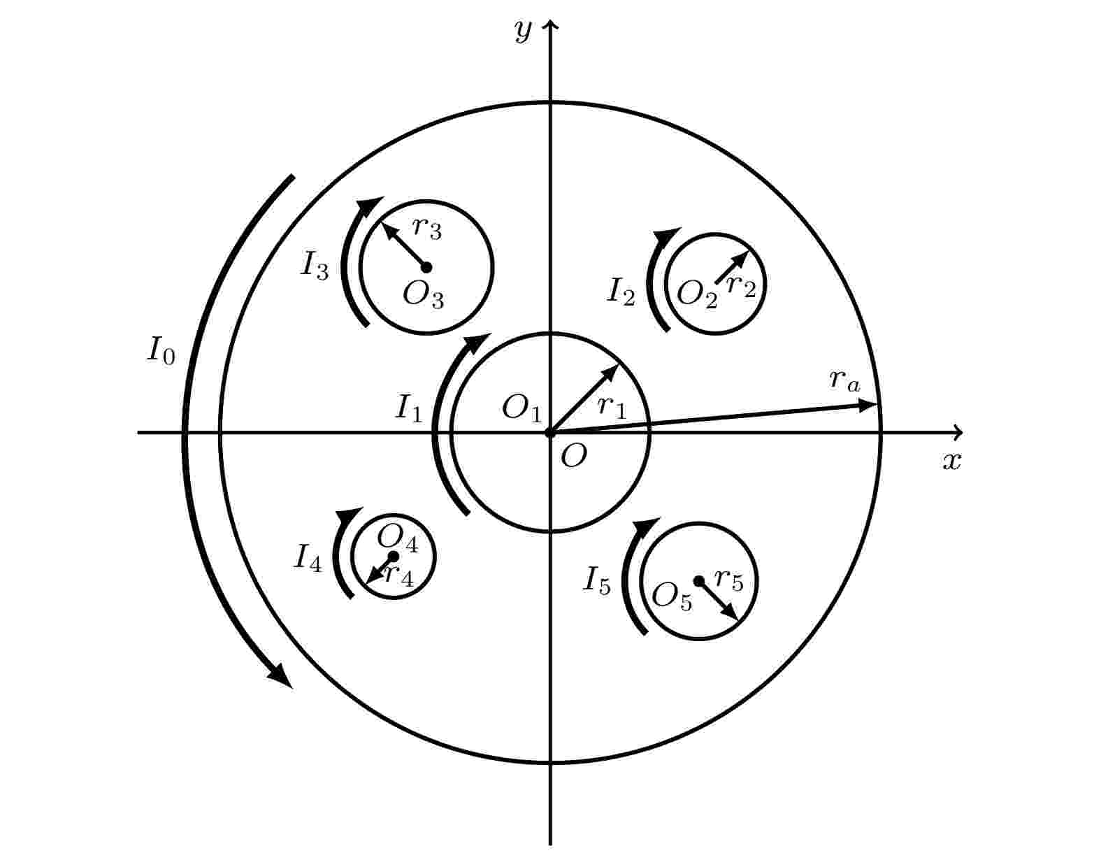
This article proposed an equivalent model to calculate the magnetic field of a special multipole magnet. The special multipole magnet is formed when two permanent magnets of large dimension differences are forced into contact with the same polarity, after the removal of the small magnet, the large magnet becomes the multipole magnet. In the process, the interacting force between the two magnets changes from repulsive force to attractive force as the two magnets approach. Moreover, the reversed pole of the multipole magnet occupies an area roughly the same as the contact area of the two magnets. Qualitatively, the large magnet possesses a lower load line than the small magnet, which suggests that the large magnet is prone to irreversible demagnetization, whereas the small magnet tends to remain unperturbed. Quantitatively, taking axially magnetized cylindrical magnets as examples, the equations for the magnetic fields were derived based on the magnetizing current theory under the assumption that the magnetization of the multipole magnet is locally homogeneous. To validate our equivalent model, two special multipole magnets (model A and model B) have been studied both theoretically and experimentally. Model A was obtained by a large magnet ($\Phi40\times2.5$ ) demagnetized at the center by a small magnet ($\Phi12\times18$ ), model B was obtained by demagnetizing model A with 4 extra small magnets ($\Phi6\times20$ ) at specific symmetrical positions around the center. Measurements for the magnetic induction intensity of the special multipole magnets are in good agreement with the theoretical calculations. The results suggested that the special multipole magnets of model A and B are equivalent to ring magnets and porous magnets, where the near field magnetic induction of the multipole magnets can be adjusted by the small magnets. In addition, a parameter analysis was carried out to study the influence of small magnets on the special multipole magnets. The results indicated that the reversed pole behavior of the special multipole magnet works mainly at positions near the magnet, and decreases rapidly as the observation point moves away from the reversed area. Our model may provide a theoretical basis and alternative solutions for electromechanical systems using multipole magnets.
2021, 70 (16): 167801.
doi: 10.7498/aps.70.20210357
Abstract +
2021, 70 (16): 167802.
doi: 10.7498/aps.70.20210443
Abstract +
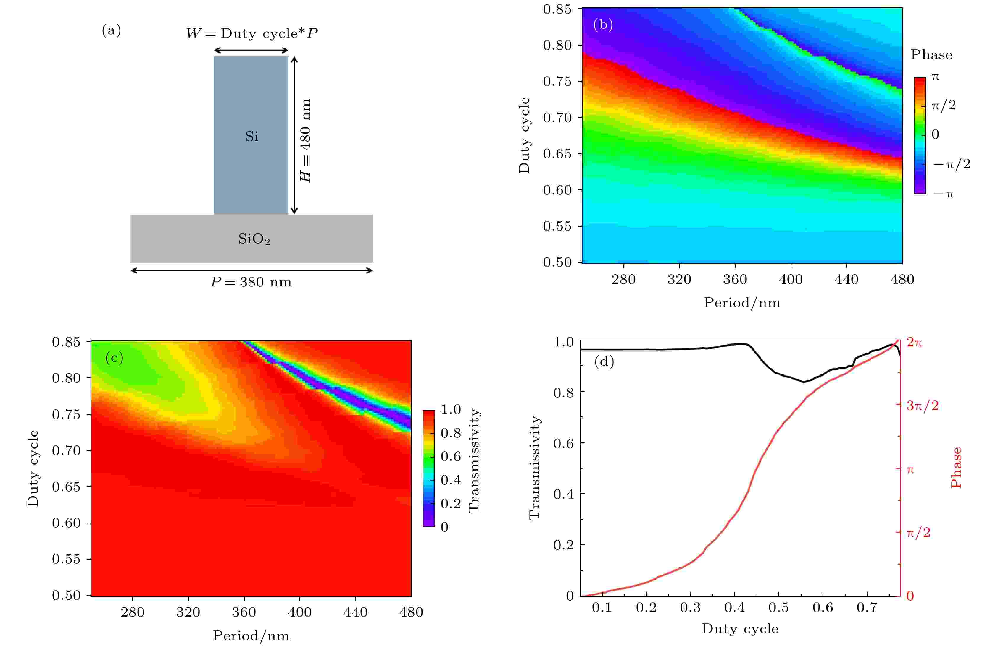
Metasurface can precisely control degrees of freedom of the phase, polarization, and amplitude of the incident light field. It provides a new way to develop the next generation of the experimental platform of quantum-state manipulation on-chip, which has important application prospects. This paper proposes a new type of metasurface structure, that is, a metalens composed of silicon grating elements with different duty ratios that can form a focusing ring on the focal plane. The intensity distribution of the ring light field in the focal plane and the focusing characteristics of metalens with different numerical apertures are studied. An optical storage ring of magnesium fluoride (MgF) molecule is constructed by using this kind of metalens focusing ring. The optical potential and dipole force of the MgF molecule in the focused light field are calculated, and the dynamic process of MgF molecule motion in the storage ring is simulated by the Monte-Carlo method. The research results show that for the incident light of 1064-nm radially polarized light, the designed metasurface structure has good focusing characteristics, and the light field intensity of the focusing ring is 55.1 times stronger than that of the incident light. The focal length of the annular light field is 22 μm and the full width at half maximum of the light intensity distribution in the focal plane is 0.8 μm, and the numerical aperture of the hyperlens is 0.69. The maximum dipole potential of MgF molecules in the light field is 32 μK, which can realize the loading of MgF molecules and trap them in the surface storage ring.
EDITOR'S SUGGESTION
2021, 70 (16): 167803.
doi: 10.7498/aps.70.20210438
Abstract +
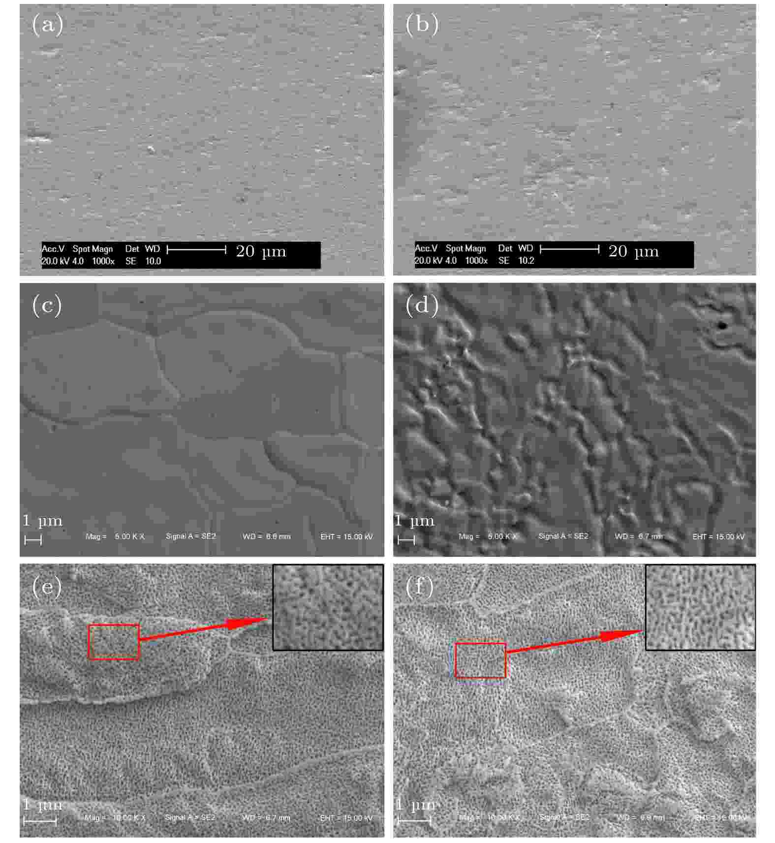
Pure tungsten (W) is a primary plasm-facing material (PFM) candidate because of its superior properties, but it still has some drawbacks. In order to solve these problems, various methods have been used to improve the performances of tungsten-based materials. Potassium (K) doping, as one of the typical dispersion-strengthening methods for W materials, improves low temperature brittleness, reduces the ductile-brittle transition temperature, and suppresses the recrystallization. Meanwhile, it also improves the thermal shock resistance and fracture toughness of the material by introducing nano-sized K bubbles. However, this method brings a large number of defects inevitably. In fact, the K bubbles and the dislocations which are pinned by these K bubbles can affect the morphology and evolution of hydrogen (H) and helium (He) atoms in the alloys. As a very sensitive method to detect vacancy-type defects in materials, positron annihilation spectroscopy is used to study the irradiation damage caused by H and He atoms in this paper. The calculation of positron lifetime shows that positrons are more sensitive to the vacancy-type defects. Bounding of H and He with vacancies reduces the positron lifetime because of the increase of valence electron density. Combining the calculated results with the positron annihilation lifetime spectrum (PLAS) results shows that the W-K alloy is easier to promote the H atoms to release. Besides, it also more likely to form larger He bubbles which can be estimated by positron lifetime values. The result is also confirmed by the measurements from the scanning electron microscope (SEM) and slow positron Doppler broadening spectroscopy (DBS). The defects in the W-K alloy such as K bubbles and their pinned dislocations can act as diffusion channels to promote the H atoms to release, which gives rise to a smoother surface under the pure H irradiation. Meanwhile, under the condition of the H+6%He irradiation, the K bubbles and their pinned dislocations in the W-K alloy become the capture center of He atoms, promote their nucleation and grow into larger He bubbles. Moreover, under the action of stress and temperature gradient, some of the He bubbles migrate to the surface and release, this process is conducive to the recovery of related defects and the reduction of radiation damage.
INTERDISCIPLINARY PHYSICS AND RELATED AREAS OF SCIENCE AND TECHNOLOGY

2021, 70 (16): 168101.
doi: 10.7498/aps.70.20210062
Abstract +

EDITOR'S SUGGESTION
2021, 70 (16): 168201.
doi: 10.7498/aps.70.20202130
Abstract +
In recent years, the cathode materials of magnesium ion batteries have become a hot point of research, and the improvement of high-rate performance and cycle stability has become the main research goal. In this paper, sodium manganese oxide (Na0.55Mn2O4·1.5H2O) nanomaterial with a blended structure of nanowires and nanosheets is prepared by the hydrothermal method. The structure and morphology of the material are analyzed by X-ray diffraction and scanning electron microscopy. The variable rate charge-discharge curves and variable scan rate cyclic voltammetry curves are obtained by a battery tester and electrochemical workstation, respectively. The results show that the hydrothermal reaction time has significant effects on phase structure and morphology composition of the material. The nanosheets and nanowires in the sample form a closely blend by 72-h hydrothermal reaction (NMO-72), and the nanosheets effectively fill into the intersecting space of the nanowires. In this way, the tap density of the material is improved. More importantly, NMO-72 has higher discharge specific capacity and rate cycling performance. At a current density of 50 mA·g–1, the discharge specific capacity of NMO-72 reaches 229.1 mAh·g–1. At a current density of 1000 mA·g–1, the discharge specific capacity of the NMO-72 stabilizes at 81 mAh·g–1. When the current density returns to 50 mA·g–1 again, the discharge specific capacity remains stable at 164.7 mAh·g–1. Besides, the cyclic voltammetry test shows that the NMO-72 material has more excellent magnesium ion diffusion kinetic performance than other materials. Therefore, the NMO-72 material has more excellent reversible specific capacity, high rate performance and cycling stability.
EDITOR'S SUGGESTION
2021, 70 (16): 168501.
doi: 10.7498/aps.70.20210368
Abstract +
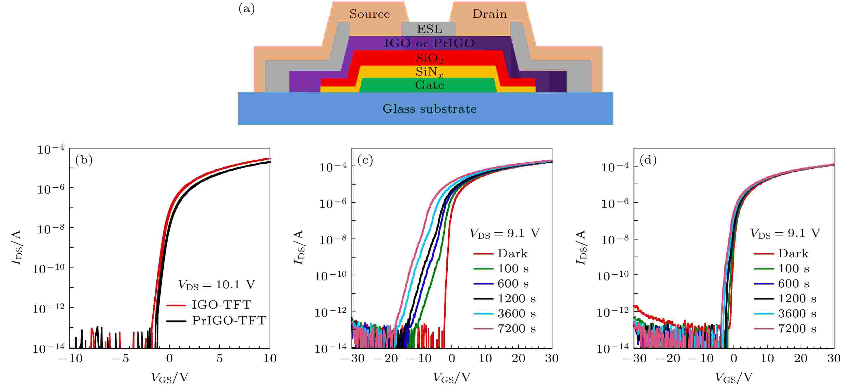
Metal oxide thin film transistors (MOTFTs) have been extensively investigated in the display industry because of their attractive characteristics, including high performances, low processing temperatures, and simple fabrication. However, under the actual working condition, the characteristics of TFTs are easily affected by the light irradiation caused the negative gate bias stress (NBIS). Therefore, the NBIS stability of MOTFT is a crucial issue that must be solved before their commercialization into an optoelectronic device. In this article, praseodymium-doped indium gallium oxide (PrIGO) is employed as the channel layer of thin film transistor (TFT). The TFTs with Pr doping exhibit a remarkable enhancement in NBIS stability. The structure and chemical composition of PrIGO film are analyzed by X-ray diffraction (XRD) and X-ray photoelectron spectroscopy (XPS), respectively. Besides, to further explore the mechanism for the improvement of NBIS stability, the low-frequency noise characteristics of IGO-TFT device and PrIGO-TFT device are studied. According to the low frequency noise characterization and analysis results, the correspondence between the normalized drain current noise power spectral density($ S_{\rm ID}/I_{\rm DS}^2 $ ) and frequency shows 1/fγ (γ ≈ 0.8) low frequency noise behavior for IGO-TFT device and PrIGO-TFT device. In addition, by studying the influences of different channel lengths on the low frequency noise of the IGO-TFT and PrIGO-TFT devices, it can be concluded that the low frequency noise of the device comes mainly from the channel region rather than from the source/drain contact region. In the linear region of the IGO-TFT device and PrIGO-TFT device, according to the linear fitting of the $ S_{\rm ID}/I_{\rm DS}^2 $ versus the overdrive voltage (VGS – Vth), it is proved that the low frequency noise of the IGO-TFT device and the PrIGO-TFT device are mainly affected by the carrier number fluctuation model. Finally, based on the carrier number fluctuation model, the defect state density at the interface between active layer and gate insulating layer is extracted to be 7.76 × 1017 cm–3·eV–1 and 9.55 × 1017 cm–3·eV–1 for IGO-TFT and PrIGO-TFT devices, respectively. We speculate that the Pr element can induce defect states in the IGO system, and the trap states induced by Pr ions facilitate the capture of free electrons by positively charged oxygen vacancies, which lead the photo-induced carrier in conduction band to be suppressed.
2021, 70 (16): 168701.
doi: 10.7498/aps.70.20210084
Abstract +
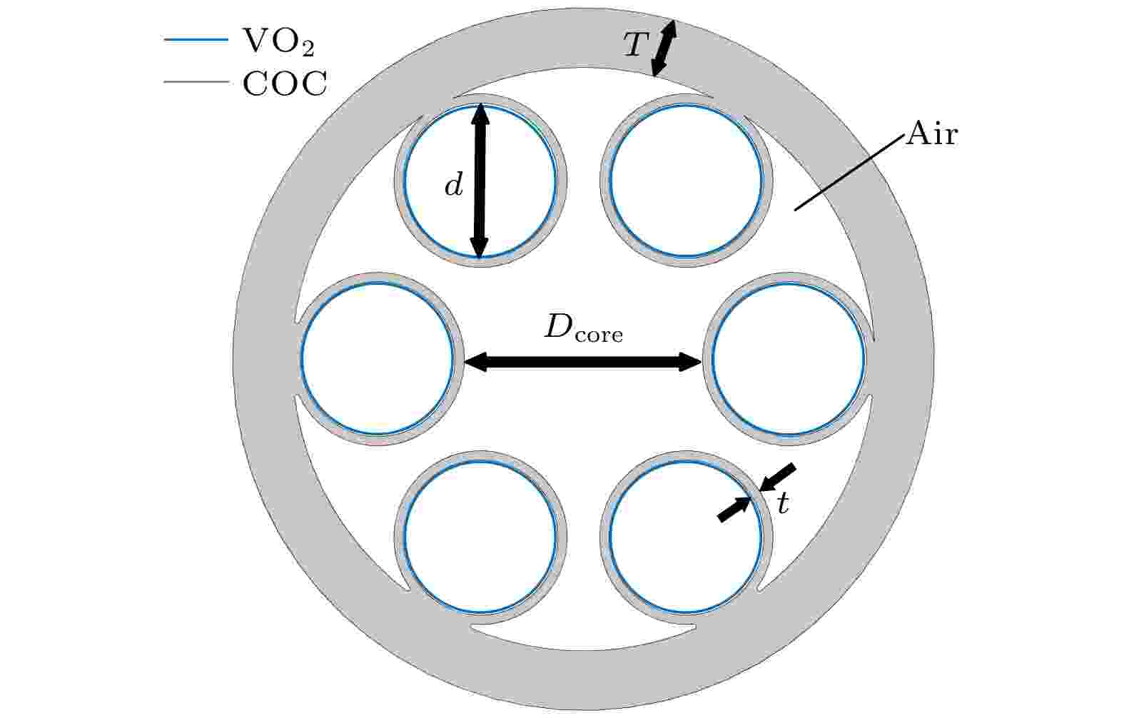
Terahertz (THz) wave is an electromagnetic wave with frequency in a range of 0.1–10 THz, which possesses excellent photonic and electronic properties. THz wave has higher penetration and lower photon energy to non-polar materials, which makes it possess great academic value in medical, non-destructive testing and other related fields. In addition, the features such as wide bandwidth and large communication capacity of THz wave allow it to be widely used in communication, radar detection and other applications. Despite its rapid development in recent years, THz technology is used still mainly in free space currently and it is difficult to control the transmission direction of THz wave over a long distance in free space. What is more, the transmission of THz waves in free space is affected usually by the dust and water vapor. For achieving the efficient transmission of THz waves, researchers have proposed a variety of THz waveguides, including plastic fiber, Bragg fiber, photonic crystal fiber and anti-resonant fiber (ARF). The ARF confines the incident beam within the air hole of fiber center by the anti-resonance effect, which has aroused great interest because of its simple structure, low transmission loss, high damage threshold, low dispersion, and high transmission bandwidth. At present, adjustable THz fiber devices based on ARF are still reported rarely. In the near-infrared band, researchers have combined ARF with vanadium dioxide (VO2) to realize the exceptional modulation effects. The VO2 is a metal oxide with insulator-metal phase transition when the ambient temperature is near 68 ℃, in which its electrical conductivity, dielectric constant and other properties will change drastically. In this paper, the VO2 is coated on the inner wall of the THz ARF cladding tubes, and the effect of the phase transition of VO2 on the propagation characteristics of the ARF is studied. Simulation results indicate that in the THz band, the phase transition of VO2 will cause the anti-resonance period of the ARF to change greatly, in which the confinement effect of the ARF cladding tubes on the incident beam is converted from anti-resonant state to resonant state. Without changing the structure of the ARF, the effective modulation on the THz wave in the core of the ARF can be achieved only by controlling the phase transition of VO2, which has a wide application prospect in the field of THz adjustable devices. In this paper, a THz optical switch and a polarization controller based on VO2-coated ARF are proposed. With the optical switch being on and off, the corresponding losses are 0.5 dB/m and 110 dB/m respectively at 120 μm. If phase transition of VO2 is induced by the excitation laser, it is expected to realize a fast-optical switch. Regarding the polarization controller, the polarization state and polarization direction of the THz wave in the core of the ARF can be controlled, and the birefringence coefficient of the ARF in the polarization state is more than 1.4 × 10⁻⁴.
2021, 70 (16): 168702.
doi: 10.7498/aps.70.20210403
Abstract +
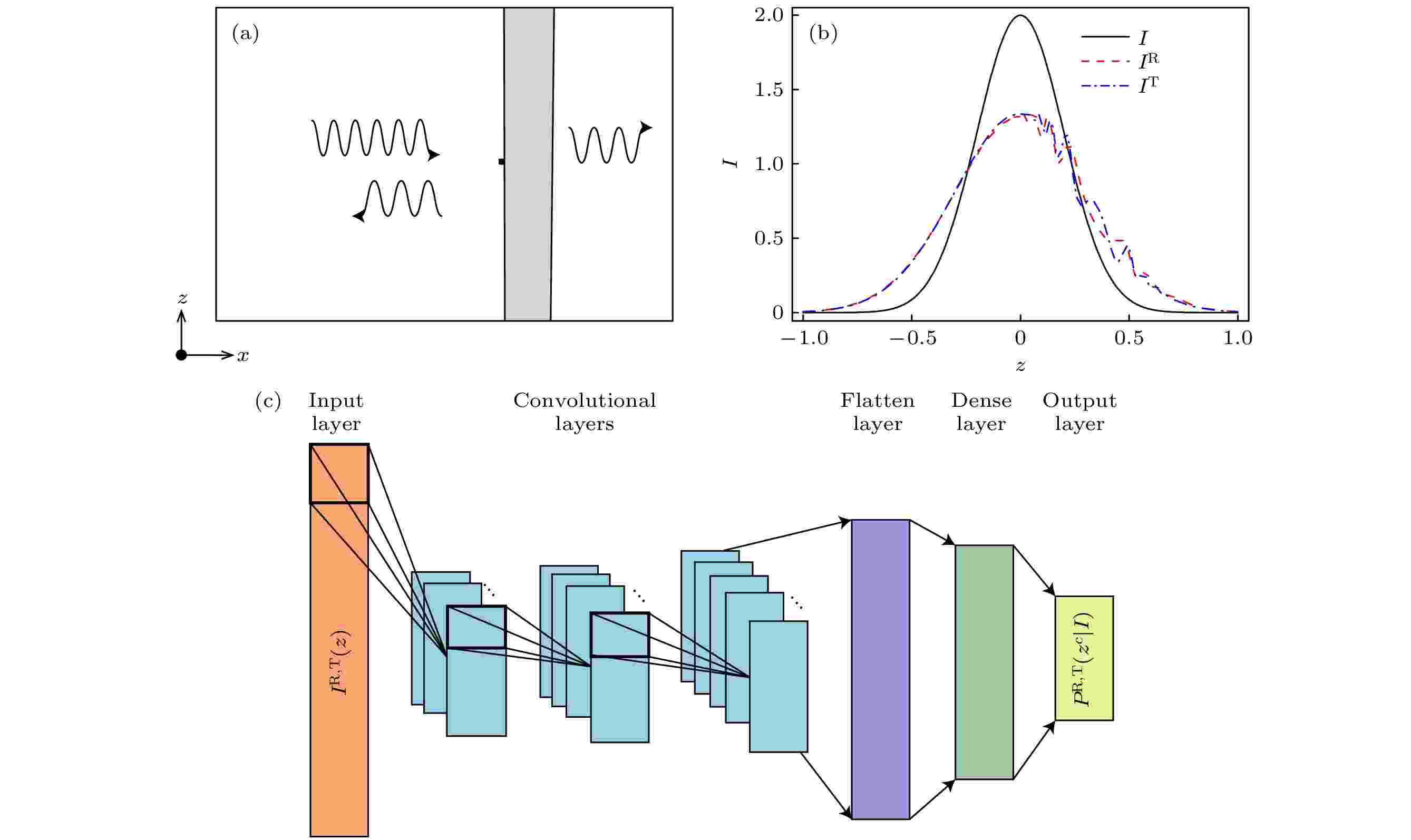
Laser technology plays fundamental roles in the modern optical experiments and applications. The performance of optical devices will be significantly affected by micro impurities and defects on the optical surfaces. Therefore, precisely positioning the optical impurities and defects is an important issue in optics. In this paper, we theoretically propose to adopt the deep learning neural networks in addressing this problem. Specifically, we generate the training data via simulating the dynamic process in which a probe optical pulse being scattered by a micro-impurity on an optical surface, and then the position information of the impurity carried by the reflection and the transmission signal can be efficiently learned by a deep convolutional neural network. One step further, we show that the deep neural network can make precise predictions on the generalization datasets generated through varying the size, refractive index, and geometry of the impurity, respectively. Additionally, we also compared the learning capability of two different networks architectures. This work provides new perspective for the impurity and defect detections in the field of precision optics.
Effects of CH3NH3 polymer formation on performance of organic-inorganic hybrid perovskite solar cell
2021, 70 (16): 168801.
doi: 10.7498/aps.70.20210353
Abstract +
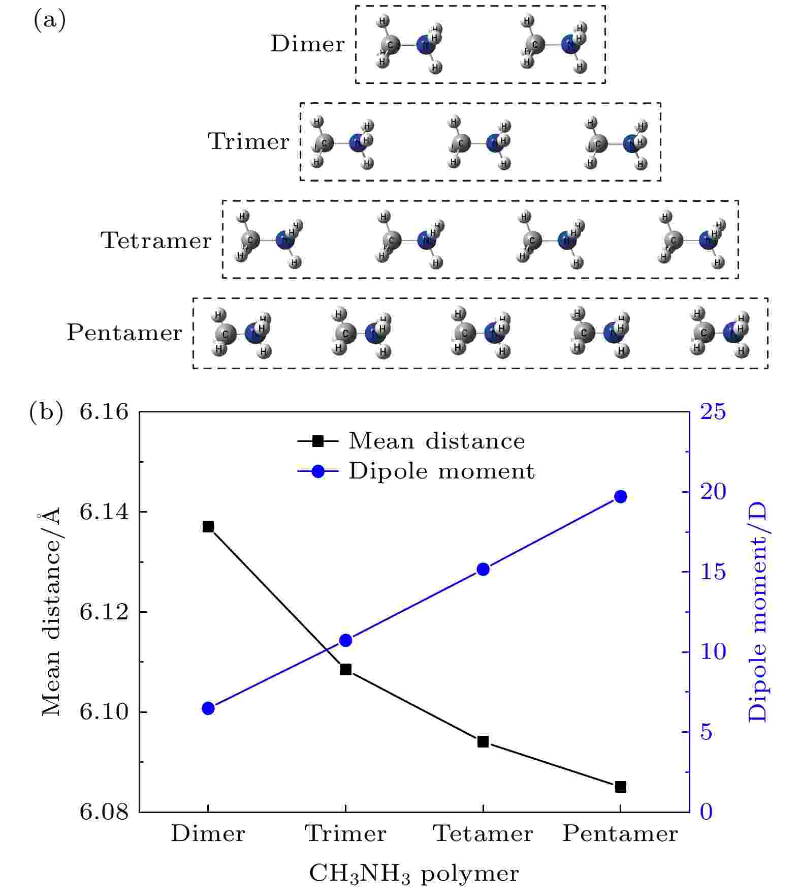
CH3NH3PbI3 is one of the most promising candidates for high-performance hybrid organic-inorganic perovskite solar cells. The CH3NH3PbI3 single crystal and polycrystalline thin film exhibit the unique features of long carrier lifetimes and diffusion lengths, however, their carrier mobilities are in fact rather modest in a range from 1 cm2·V–1·s–1 to 100 cm2·V–1·s–1. Experimentally, the temperature dependence of mobility is described as T–1.3 to T–1.6 due to the acoustic phonon scattering. To be sure, the rotating CH3NH${}_3^+ $ cations are disadvantageous to the carrier transport and performance for CH3NH3PbI3 solar cells. The effect of the rotating CH3NH${}_3^+ $ cations on high-performance CH3NH3PbI3 solar cells remains an open question. The Gaussian 09 software has been utilized to optimize the geometrical structures of CH3NH3 dimer, trimer, tetramer, and pentamer in isolated state at the MP2 level with using the cc-PVTZ basis set. For CH3NH3 polymer, the mean distance between two centroids of neighboring CH3NH3 decreasing with the number of CH3NH3 is slightly smaller than the lattice constant 6.28 Å of tetragonal CH3NH3PbI3, which is advantageous to structural stability and higher structural order of inorganic [PbI3]– framework. It signifies that the long range order of electrically neutral CH3NH3 is easily formed for room-temperature CH3NH3PbI3. The total dipole moment linearly increases with the number of CH3NH3 for CH3NH3 polymer, and attains a large value 19.7 Debye for CH3NH3 pentamer, which may be the origin of strong polarization in CH3NH3PbI3 heterojunction. The molecular orbitals of five unpaired electrons for CH3NH3 pentamer are distributed around NH3-sides of five different CH3NH3 pentamers respectively, and these orbital energies are in a range from –4.4 eV to –3.2 eV. The unpaired electrons in CH3NH3 polymer have an electrostatic attraction on the CH3-side of neighboring CH3NH3, which is the key cause of forming the ordered CH3NH3 polymer. Hence it can be inferred that the orbital energies of unpaired electrons are getting closer when the longer range order of CH3NH3 are formed in room-temperature CH3NH3PbI3 through the interfacial electron injection. The vector field map of electrostatic potential (ESP) shows that CH3NH${}_3^+ $ has strong electrophilic character, and the NH3-side has a stronger electrophilic character than CH3-side, however, CH3NH3 monomer and polymer have weak electrophilic and nucleophilic character. Thus, the forming of CH3NH3 polymer at the CH3NH3PbI3 heterojunction leads the organic and inorganic portions to be decoupled, which can effectively reduce the anharmonic phonon modes. Under an applied electric field, the unpaired electrons in CH3NH3 pentamer can transfer along the C-N axis through the hopping mechanism. According to these results, we can draw three useful conclusions below. i) The electrons under an applied electric field are easily injected into the CH3NH3PbI3 material through the heterojunction, the CH3NH3 polymer is easily formed, and the unpaired electrons in polymer are transferred between two neighboring CH3NH3 through hopping mechanism. ii) The decoupling between organic CH3NH3 and inorganic [PbI3]– framework can effectively reduce the anharmonic phonon modes, which can lead the carrier scattering decrease and the efficiency of carrier separation and transport to improve; iii) The ordered CH3NH3 polymer at the CH3NH3PbI3 heterojunction can enhance the order of inorganic [PbI3]– framework. Our researches may help to further understand the origin of high power conversion efficiency (PCE) for hybrid organic-inorganic perovskite solar cells.

2021, 70 (16): 168802.
doi: 10.7498/aps.70.20210134
Abstract +
Methylamine lead iodide (CH3NH3PbI3 MAPbI3) and formamidine lead iodide (CH(NH2)2PbI3 FAPbI3) are the most commonly used organic lead iodine perovskite materials for solar cell research. For the perovskite solar cell with a layered structure, the optical properties and thickness of each layer affect the photoelectric conversion efficiency of the cell. In this paper, the optical admittance method and rigorous coupled wave analysis method are used to calculate the absorptivities and transmittances of metal oxide transparent conductive films for tin-doped indium oxide (In2O3:Sn), fluorine-doped tin oxide (SnO2:F), TiO2, MAPbI3 and FAPbI3. The influence of each layer thickness and device structure on the short-circuit current density of the cell are analyzed. It is shown that for the FTO(ITO)/TiO2/MAPbI3 structure, when the thickness of the FTO film is 50–450 nm and the thickness of the ITO film is 10–150 nm, the average transmittance for the 360–800 nm wavelength light is 85%. For the FTO(ITO)/TiO2/FAPbI3 structure, when the thickness of the FTO film and ITO film are 50–250 nm and 10–150 nm, respectively, the average values of the transmittance for the 360-840 nm wavelength light are 81.6% and 78%, respectively. Under the optimal thickness of FTO and TiO2, and the thickness of MAPbI3 and FAPbI3 are 300–1000 nm, the corresponding short-circuit current densities are in a range of 21.9–23.7 and 23.0–24.4 mA·cm–2, respectively. The band gap of MAPbI3 and FAPbI3 are 1.56 and 1.48 eV, for which the corresponding absorption cut-off wavelengths are 796 and 840 nm, respectively, indicating that FAPbI3 has a wider absorption spectrum than MAPbI3. In order to maximize the Jsc value of the organic lead iodine perovskite solar cell, the thickness range of each layer for MAPbI3 perovskite solar cell (FTO thickness is (80 ± 50) nm, ITO thickness is less than 120 nm, MAPbI3 thicknessis 300–600 nm) and for FAPbI3 perovskite solar cell (FTO thickness is (120 ± 50) nm, ITO thickness is less than 180 nm, FAPbI3 thickness is 300–600 nm) are given. The research results of this article have guiding significance in designing and preparing the perovskite solar cells with high conversion efficiency.


