Vol. 71, No. 19 (2022)
2022-10-05
GENERAL
2022, 71 (19): 190201.
doi: 10.7498/aps.71.20220833
Abstract +
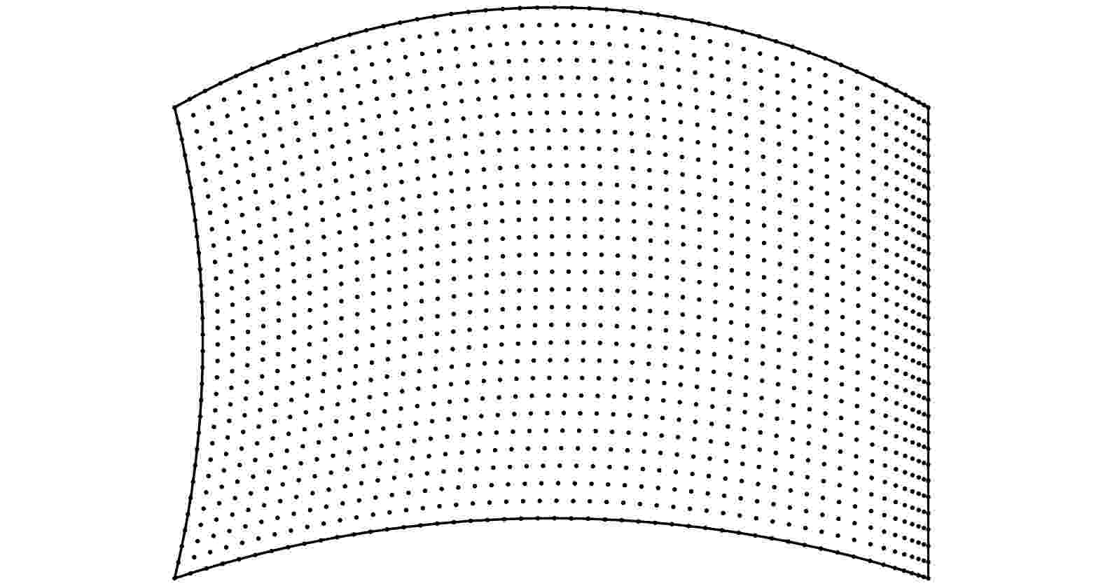
In this paper, a completely new numerical method, called finite line method, is proposed and is used to solve fluid-solid coupled heat transfer problems. The extensively used finite element method is a method based on volume discretization; the finite volume method is a method operated on the surface of the control volume; the boundary element method is the one based on boundary surface discretization; the meshless method is the one constructing the computational algorithm using surrounding scatter points at a collocation point. The method proposed in the work is based on the use of finite number of lines, in which an arbitrarily high-order computational scheme can be established by using only two or three straight or curved lines at each point. The creative idea of the method is that by using a directional derivative technique along a line, high-order two- and three-dimensional spatial partial derivatives with respective to the global coordinates can be derived from the Lagrange polynomial interpolation formulation, based on which the discretized system of equations can be directly formed by the problem-governing partial differential equation and relevant boundary conditions. The proposed finite line method is very simple in theory and robust in universality, by using which the boundary value problems of partial differential equations in solid and fluid mechanics problems can be solved in a unified way. In solving fluid mechanics problems, the diffusion term is simulated by using the central line set to maintain a high efficiency, and the convection term is computed by using an upwind line set to embody its directional characteristic. A few of numerical examples will be given in this paper for fluid-solid coupled heat transfer problems for verifying the correctness and efficiency of the proposed method.

2022, 71 (19): 190301.
doi: 10.7498/aps.71.20220331
Abstract +
Boson sampling is a candidate for quantum protocols to truly realize the quantum computation advantage and to be used in advanced fields where complex computations are needed, such as quantum chemistry. However, this proposal is hard to achieve due to the existence of noise sources such as photon losses. In order to quantificationally analyze the influences of photon losses in optical networks, boson sampling is classically simulated based on the equivalent beam splitter mechanism, where the photon loss happening in optical units is equivalent to the photon transmission into the environmental paths through a virtual beam splitter. In our simulation, networks corresponding to random unitary matrices are made up, considering both the Reck structure and the Clements structure. The photon loss probability in an optical unit is well controlled by adjusting the parameters of the virtual beam splitter. Therefore, to simulate boson sampling with photon losses in optical networks is actually to simulate ideal boson sampling with more modes. It is found that when the photon loss probability is constant, boson sampling with Clements structures distinctly performs much better than that with Reck structures. Furthermore, the photon loss probability is also set to follow the normal distribution, which is thought to be closer to the situation in reality. It is found that when the mean value of photon loss probability is constant, for both network structures, errors of outputs become more obvious with the increase of standard deviation. It can be inferred that the increase of error rate can be explained by the network depth and the conclusion is suitable for larger-scale boson sampling. Finally, the number of output photons is taken into consideration, which is directly related to the classical computation complexity. It is found that with the photon loss probability, the ratio of output combinations without photon losses decreases sharply, implying that photon losses can obviously affect the quantum computation advantage of boson sampling. Our results indicate that photon losses can result in serious errors for boson sampling, even with a stable network structure such as that of Clements. This work is helpful for boson sampling experiments in reality and it is desired to develop a better protocol, for example, a well-designed network or excellent optical units, to well suppress photon losses.

Stochastic resonance in asymmetric bistable coupled network systems driven by Gaussian colored noise
2022, 71 (19): 190501.
doi: 10.7498/aps.71.20220909
Abstract +
In this work studied is the synergistic effect of asymmetric bistable coupled network systems under the action of Gaussian colored noise and periodic signal. The system is a network model consisting of a large number of oscillators. The interaction and change between individuals produce complex nonlinear behavior patterns. For further research, firstly, the original N-dimensional system is reduced and approximated by using the mean field theory, the unified colored noise approximation theory and the equivalent nonlinearization method. Secondly, the Langevin equation of simplified model is obtained through the slaving principle by using the two-state model theory to derive the theoretical expression of signal-to-noise ratio. It is found that the system produces the phenomenon of scale stochastic resonance. Finally, the effects of Gaussian color noise parameters, system parameters and periodic signal parameters on the stochastic resonance behavior of asymmetric coupled network systems are discussed. The results show that the increase of Gaussian colored noise correlation time and noise intensity can promote the scale stochastic resonance phenomenon; selecting appropriate coupling coefficient can achieve the optimal stochastic resonance effect. And the stochastic resonance phenomenon of the system driven by the Gaussian colored noise and the Gaussian white noise, respectively, are analyzed and compared with each other. Research result shows that Gaussian colored noise is more conducive to enhancing stochastic resonance phenomenon.

EDITOR'S SUGGESTION
2022, 71 (19): 190502.
doi: 10.7498/aps.71.20220904
Abstract +
In this paper, a four-terminal hybrid driven refrigerator model with three capacitively coupled quantum dots is proposed, which can be driven by the energy current injected from the highest temperature thermal reservoir and the power input to achieve the refrigeration of the low temperature reservoir. Based on the master equation we derive the expressions for charge current and heat current between three quantum dots and thermal reservoirs in the weak/strong capacitive coupling case, respectively. We numerically analyze the thermodynamic performance characteristics of the refrigerator between the cooling rate and the coefficient of performance, and the main performance parameters of the refrigerator are optimized under the condition of the maximum cooling rate. Finally, we compare the performance of this refrigerator in the strong capacitive coupling case with that in the weak capacitive coupling case.
NUCLEAR PHYSICS
2022, 71 (19): 192101.
doi: 10.7498/aps.71.20220929
Abstract +
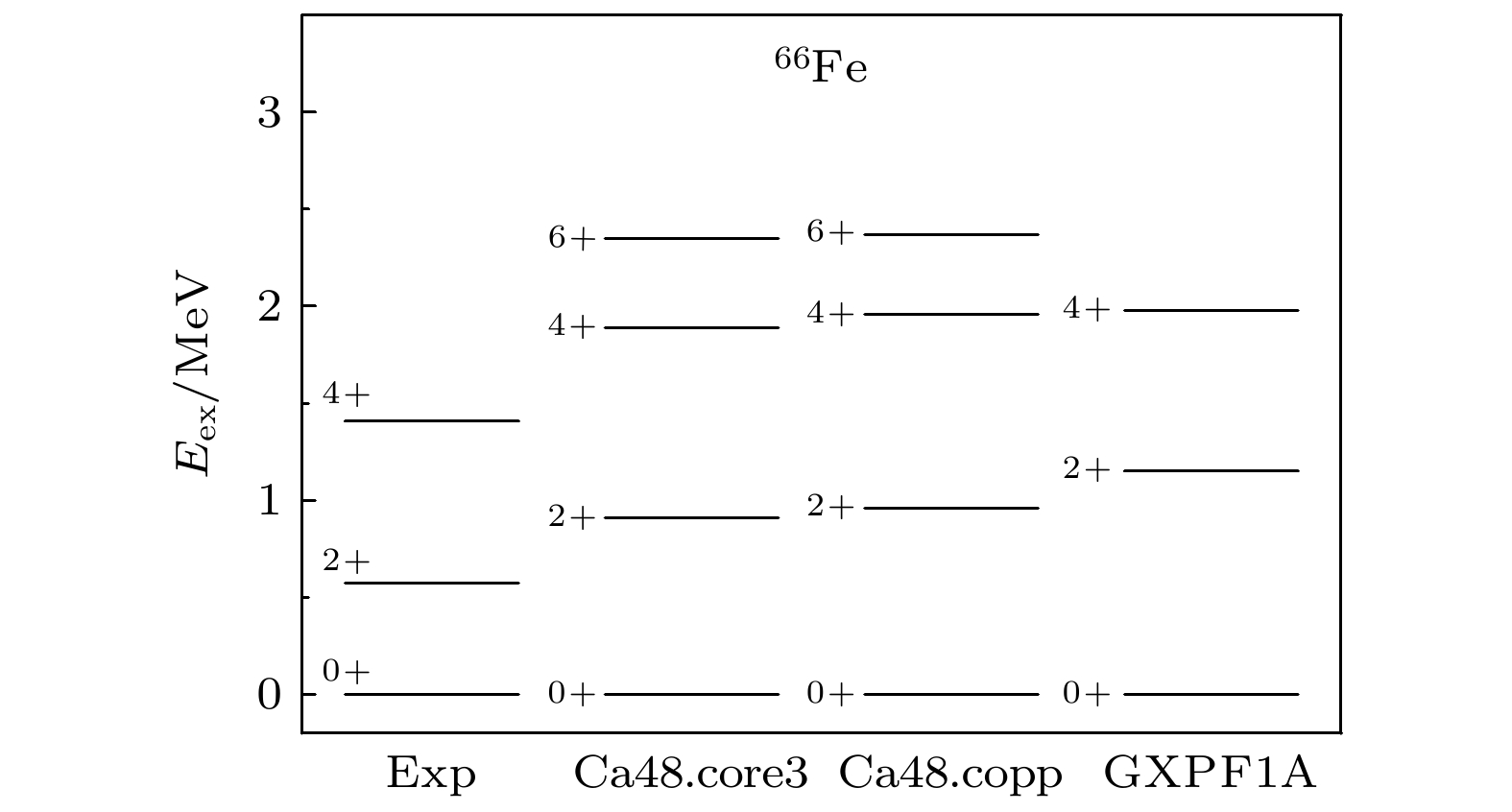
The calculation of weak interaction rates plays a very important role in studying nuclear physics and nuclear astrophysics. In this work, we calculate the electron capture rate of 66Fe in the framework of shell model. We mainly focus on the contribution of allowed transition and forbidden transition to the total rate. It is found that in some astrophysical environments the forbidden transition is very important in contribution to the electron capture rate, in which the non-unique forbidden transition plays a major role. This is very important for nuclear structures and astrophysics.

EDITOR'S SUGGESTION
2022, 71 (19): 192501.
doi: 10.7498/aps.71.20220776
Abstract +
Natural iridium acts as a high-quality activated detector for probing the energy components of a neutron fluence. Measurements of 191Ir(n,2n)190Ir cross sections are carried out near 14 MeV by the activation method based on 93Nb(n,2n)92mNb reaction cross section standard by PD-300 neutron generator DT neutron source. The (n,2n) products are measured by using a calibrated high pure Ge detector. The cross sections of 191Ir(n,2n)190Ir, σm2 and σg+m1, are measured carefully. The 191Ir(n,2n)190Ir cross sections: σm2, σg+m1, σg+m1+m2 and cross section ratio of σm2/σg+m1 are obtained in an energy range of 13.40–14.86 MeV. Experimental uncertainties are in a range of 3.4%–3.5%. The measured cross sections for the reaction of 191Ir(n,2n)190Ir at 14 MeV are σm2 = (136.05 ± 4.93) mb, σg+m1 = (1972.35 ± 67.06) mb, σg+m1+m2 = (2108.40 ± 71.99) mb, and σm2/σg+m1 = 0.0690 ± 0.0024. The present data are compared with the previous experimental data and the ENDF/B-VIII.0 and JEFF3.0/A evaluated data, showing that the experimental data from the literature are in good agreement with the present data for σg+m1, the evaluated data from JEFF3.0/A are underestimated by 5%–20% in comparison with the present data for σm2, the evaluated data from ENDF/B-VIII.0 are underestimated by 10% in comparison with the present data for σm2, and the ENDF/B-VIII.0 data are consistent with the present data for σg+m1+m2. The discrepancies between the data from the literature and the present data are analyzed and clarified. The present data show significant improvement in accuracy in comparison with data from the literature, these results provide more reliable nuclear data for improving the future evaluation.
2022, 71 (19): 192801.
doi: 10.7498/aps.71.20220530
Abstract +
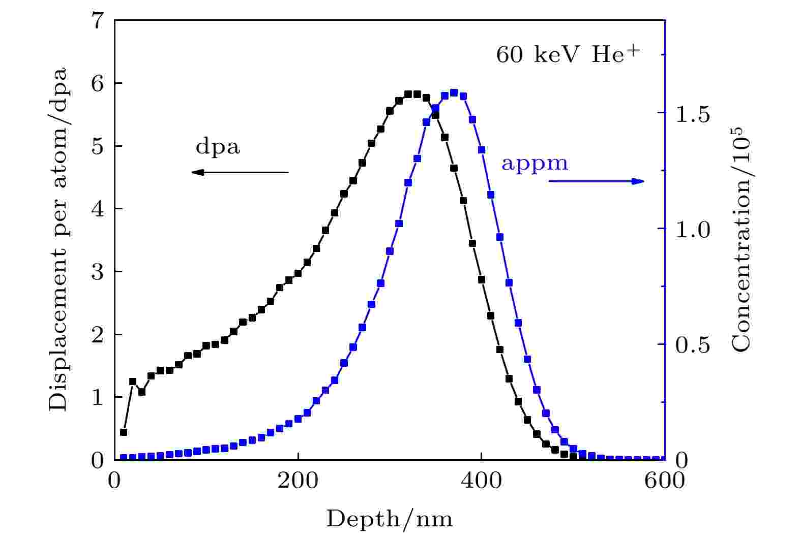
Since the 21st century, low atomic number material coating has been considered as one of methods for treating the first wall of controllable thermonuclear fusion device . The TiB2 material with high melting point, high hardness, low coefficient of thermal expansion, excellent wear resistance and low atomic number has entered into people’s field of vision. Single TiB2 is difficult to sinter and process into other products. Therefore, adding ceramic and metal additives to TiB2 matrix material to effectively improve the mechanical properties and processability of the material has become a research hotspot. On the basis of the existing researches of TiB2-SiC, in the present work the metal Ti powder is added as the second additive to improve the properties of TiB2 composite. The TiB2 and SiC are mixed at a mass ratio of 2 to 3, then two kinds of TiB2-SiC-Ti materials with different amounts of Ti content are prepared by spark plasma sintering (SPS) technology. The materials are irradiated by a He+ beam with energy of 60 keV and ion fluence of 2 × 10¹⁷ ions/cm2 at room temperature. The material is heat-treated at 1500 ℃ before and also after irradiation. The performances of prepared samples, the effect of irradiation on materials and the results of high temperature heat treatment are characterized by energy dispersive spectroscopy, Raman spectrum, grazing angle x-ray diffraction spectrum, Vickers hardness, wear resistance test, and scanning electron microscope. The results show that the surface morphology and toughness of TiB2-SiC-Ti material with 3% Ti mass fraction are poor as shown in SEM images. The wear resistance test indicates that the material surface is seriously worn and the wear resistance is poor. The X-ray diffraction spectrum and Raman spectra show that the material is oxidized seriously at 1500 ℃, which is likely to be the cause of the poor compactness of materials. Raman spectra, Grazing angle X-ray diffraction spectrum and some Vickers hardness data before and after irradiation indicate that the material with low Ti content possess better crystal structure and weaker irradiation hardening. In conclusion, the TiB2-SiC-Ti material with 3% Ti mass fraction exhibits lower density, poorer wear resistance and lower hardness, while the material with lower Ti mass fraction is more resistant to irradiation than the material with 6% Ti mass fraction at room temperature.
ATOMIC AND MOLECULAR PHYSICS
2022, 71 (19): 193101.
doi: 10.7498/aps.71.20220734
Abstract +
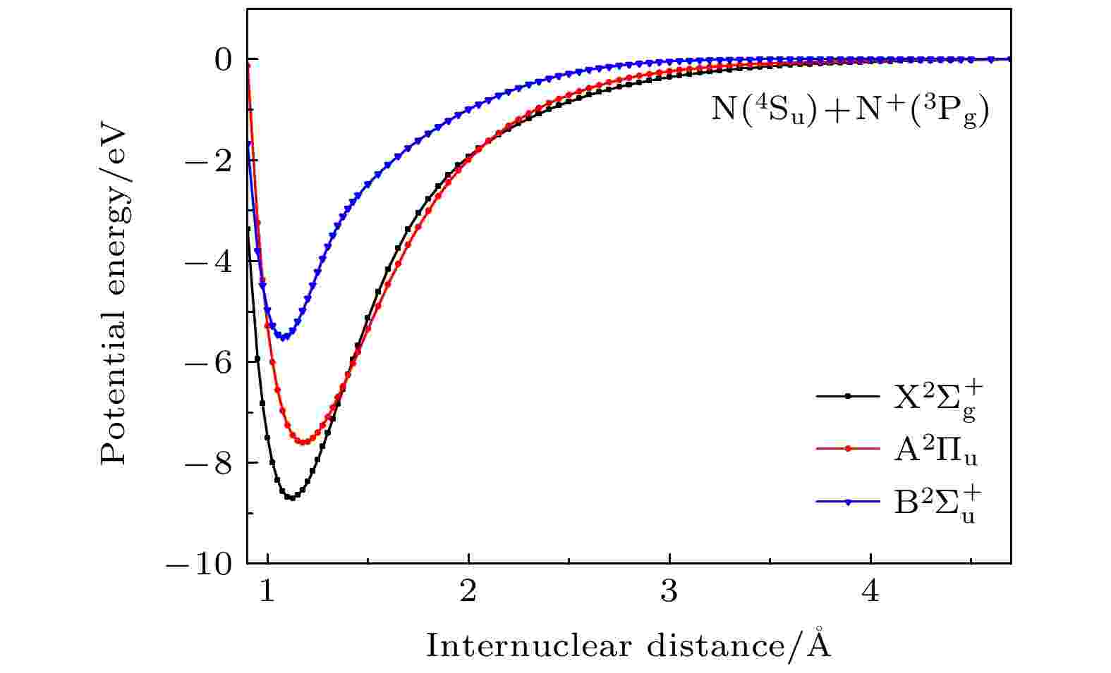
The potential curves, spectroscopic constants and dipole moments for $ {{\text{X}}^{2}}{\Sigma}_{\text{g}}^{+} $ , A2Πu and $ {{\text{B}}^{2}}{\Sigma}_{\text{u}}^{+} $ state of $ {\text{N}}_{2}^{+} $ are calculated by the internal contraction multi reference configuration interaction (icMRCI) method, with Davidson correction taken into consideration. According to the results of molecular structures, we present the partition function in a temperature range of 100–40000 K and the opacities at different temperatures (295, 500, 1000, 2000, 2500, 5000 and 10000 K) under a fixed pressure of 100 atm. It is found that the populations of excited states increase with temperature increasing, as a result, the wavelength range of opacity also increases and band boundaries for different transitions gradually become obscure. In comparison with the cases of N2 with the same pressure and temperature, significant discrepancies are found in the wavelength ranges and structures of opacity of $ {\text{N}}_{2}^{+} $ for the present work. The influence of temperature on the opacity of $ {\text{N}}_{2}^{+} $ is studied systematically in the present work, which is expected to provide theoretical and data support for astrophysics.
2022, 71 (19): 193201.
doi: 10.7498/aps.71.20221044
Abstract +
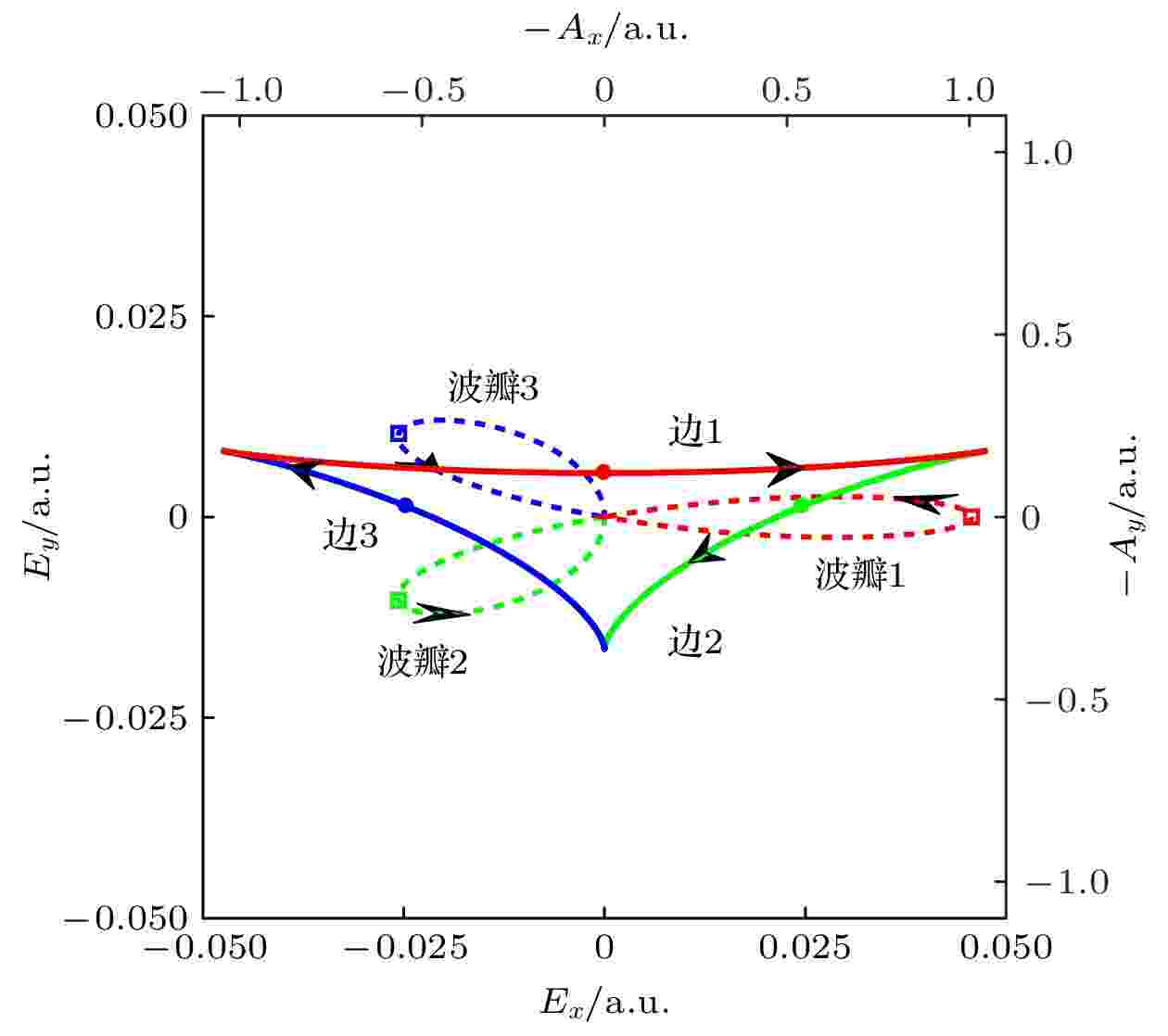
Electron correlation behaviors and recollision dynamics in nonsequential double ionization (NSDI) of Ar atoms in a counter-rotating two-color elliptically polarized (TCEP) field are investigated by using a three-dimensional classical ensemble model. The numerical results show that the correlated momentum distribution of electron pairs in the x-axis direction evolves from a V-shaped structure in the first quadrant at the low intensity, to an arc-shaped structure mainly located in the second and fourth quadrants at moderate intensity, finally to a distribution near the origin located in the first quadrant in the high intensity. With the laser intensity increasing, the dominant correlation behavior evolves from correlation to anti-correlation and finally reverts back to correlation. The combined electric field traces out a trefoil pattern, i.e. the waveform in a period shows three leaves in different directions. Each leaf is called a lobe. The electric field recursively evolves from lobe 1 to lobe 2 and to lobe 3. Unlike the counter-rotating two-color circularly polarized fields, the combined fields from two elliptical fields do not have the spatial symmetry. Amplitudes of the three field lobes and the angles between them are different. Furthermore, the back analysis of NSDI trajectories shows that the single ionization in NSDI events mainly occurs in lobe 1 and lobe 3, and the contribution from lobe 1 increases and that from lobe 3 decreases with the increase of the intensity. Correspondingly, the free electrons mainly return to the parent ion from 20° and 175°. With the laser intensity increasing, the electrons returning from 20° gradually increase and those returning from 175° gradually decrease. In order to further understand the correlation behaviors of electron pairs in the x-axis direction, the NSDI events triggered off by single ionization from different lobes are separately discussed. With the increase of laser intensity the correlation behavior of NSDI events triggered off by single ionization from field lobe 1 evolves from anti-correlation behavior to correlation behavior, but the correlation behavior of NSDI events induced by single ionization from field lobe 3 evolves from correlation behavior to anti-correlation behavior. With the laser intensity increasing, the NSDI events induced by single ionization from field lobe 1 increase gradually, but those from field lobe 3 decrease. This results in that the total dominant correlation behavior evolves from correlation to anti-correlation and finally reverts back to correlation as the laser intensity increases.
2022, 71 (19): 193301.
doi: 10.7498/aps.71.20220866
Abstract +
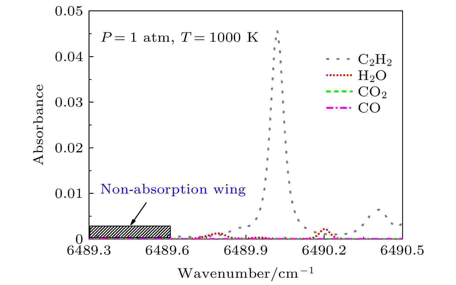
Soot particles from the combustion of hydrocarbon fuels are the main source of the air fine particles and they are also an important factor of reducing the combustion efficiency. As one of their major precursor, acetylene (C2H2) plays an important role in forming soot. So the simultaneous detecting of soot particle and C2H2 is significant in studying the mechanism of the soot formation. In this work, a sensor for the simultaneous detecting of soot particle and C2H2 is developed by using a single DFB diode laser with a wavelength near 1540 nm. The extinction spectrum near the proper C2H2 line at 6490.02 cm–1 is used to infer the mass concentration of particles and the C2H2 concentration. The performance of the sensor is confirmed in a home-made heated static cell which can provide well controlled gaseous environment and particulate environment. The measured mass concentration of particles and the C2H2 concentration are within 2.73% and 5.17% of the expected values over the full temperature range of 500–1000 K, respectively. All the measurements show the potential application of the sensor in the simultaneous detecting of soot particle and C2H2 at elevated temperature.

2022, 71 (19): 193302.
doi: 10.7498/aps.71.20220430
Abstract +
Depending on a four-level inverted-Y atomic system, we demonstrate the limitation of linewidth-narrowing for the probe absorption spectrum in the electromagnetic induced absorption platform. Thanks to the use of an auxiliary control field which couples one hyperfine ground state and one middle-excited state we show that the linewidth limitation can be constrained by a coherence decay rate between two hyperfine ground states, rather than by the decay rate between the ground and the excited states as in previous Ladder schemes. That fact makes the theoretically-predicted absorption linewidth at least two orders of magnitude narrower. By using a suitable adjustment for the control-field amplitude and the detuning we numerically show that an extremely-narrowed probe absorption spectrum accompanied by a higher spectra contrast can be obtained, which confirms well with our theoretical predictions. We study the transient time response to the absorption spectrum and show that a relatively longer response time arises due to the small coherence decay rate between two hyperfine ground states. Furthermore, we reduce the influence on linewidth-narrowing from the Doppler effect via an optimized design of lasers, and reveal that no Doppler-free effect exists due to the lack of three-photon process. Our results may pave a route to the development of high-resolution spectroscopy in current experiments.
ELECTROMAGNETISM, OPTICS, ACOUSTICS, HEAT TRANSFER, CLASSICAL MECHANICS, AND FLUID DYNAMICS
2022, 71 (19): 194101.
doi: 10.7498/aps.71.20220353
Abstract +
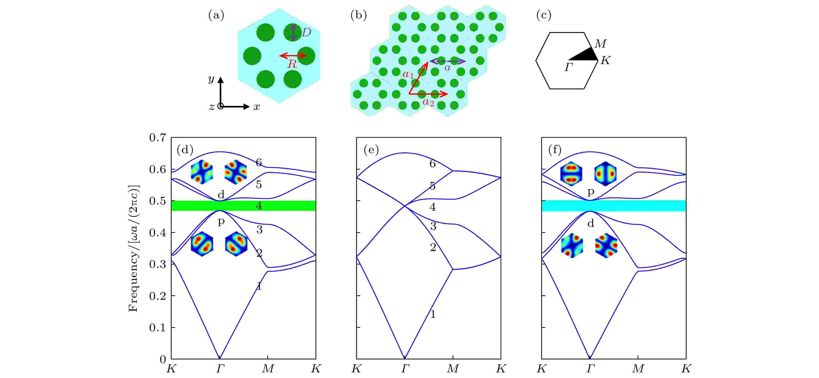
The unidirectional propagation of the pseudospin-locked optical waves can be achieved by using the helical edge states in two-dimensional topological spin photonic crystals. Although there have been lots of researches on topological spin photonic crystal, the unidirectional propagation regulation of helical edge states has been rarely studied up to now. Herein, by tuning the diameter D of the dielectric rod and the distance R between the center of the unit cell and the center of the rod in two-dimensional topological spin photonic crystal with C6v symmetry, the effects of geometric parameters on the bandgap structure, topological properties and unidirectional propagation of helical edge states in topological spin photonics crystals are studied in detail. The results show that the parameter R has significant effects on the bandgap structure and topological properties of topological spin photonic crystal, and the diameter D of rod only affects the bandgap positions. The structures of helical edge states and their unidirectional propagations are closely related to the topological properties of the bandgaps and the frequency structures of photonic crystals on both sides of boundary. Without changing the topological properties of bandgaps, only changing the structures of the photonics crystals on either side of the boundary can also regulate the structures of the helical edge states and their unidirectional propagation. Thus, by adjusting the geometric parameters R and D of the topological spin photonic crystals, the helical edge states and their unidirectional propagations can be controlled. This study provides useful references for the selection and application of helical edge states in topological spin photonic crytals.

2022, 71 (19): 194102.
doi: 10.7498/aps.71.20220599
Abstract +
2022, 71 (19): 194201.
doi: 10.7498/aps.71.20220494
Abstract +
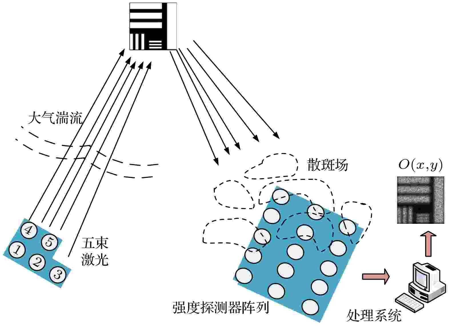
Sheared beam imaging (SBI) is considered a computational imaging technique that transmits three sheared coherent laser beamlets for illumination, and a sensor array to receive the intensity of the speckle pattern reflected from the target. The SBI can be used to image remote objects through a turbulent medium with no need of any adaptive optics. However, while imaging low-orbit moving targets, the number of detectors of sensor array required by the receiving system of SBI is very large, and the development of sensor array is difficult and costly. In this work, a spatial domain sparse sampling technique is proposed for the SBI system through transmitting five laser beamlets to illuminate the target carrying more of its spectral information, which can reduce the number of detectors of the sensor array. Firstly, the principle of the sparse imaging technique is deduced. Then, a sparse reconstruction algorithm is studied. The phase difference and amplitude information of the target in the echo signal after sparse sampling can be extracted accurately by searching for the accurate positions of the beat frequency components. The wavefront phases can be demodulated by the least-squares method, and wavefront amplitude can be obtained by the algebraic operation of speckle amplitude. The reconstructed wavefront is used to formulate the two-dimension image of the target. Theoretically, without affecting the resolution, the number of detectors of the sensor array can be reduced to half of the traditional three-beam method, which breaks through the limitation that the detector spacing of sensor array is equal to the shear length of beamlet. From the simulation results, when the number of detectors of the sensor array is reduced by 50%, the proposed sparse reconstruction algorithm has almost the same quality as the reconstructed image with the traditional three-beam method.

2022, 71 (19): 194202.
doi: 10.7498/aps.71.20220574
Abstract +
2022, 71 (19): 194203.
doi: 10.7498/aps.71.20220675
Abstract +
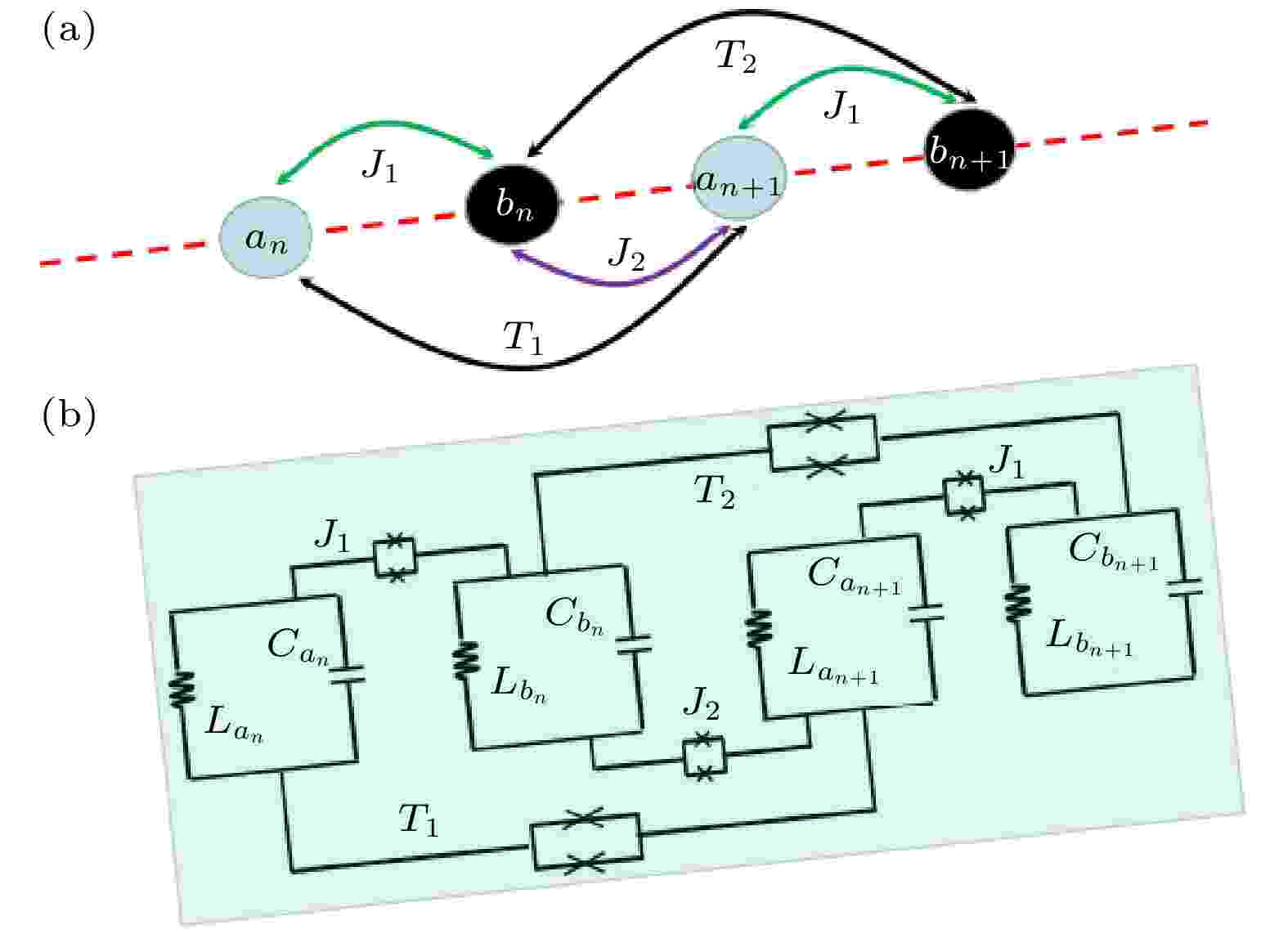
We propose a theoretical scheme for a one-dimensional lattice based on a superconducting quantum circuit system consisting of two types of superconducting microwave cavities, the interaction between nearest-neighbor and next-nearest-neighbor unit cells that can be adjusted by the magnetic flux, the system can obtain the collective dynamic evolution and study the topological properties of the system.First, we investigate the energy spectrum and edge states of the odd-even lattice size and find that the odd-even lattice number affects the topological properties of the system. Furthermore, considering the next-nearest interactions, it is found that there are constraints on the next-nearest interactions, which can be tuned to study the topological phase transitions of the system and the transfer of topological quantum states.In addition, considering the influence of defects on topological properties, it is found that the defect potential energy is small, the system energy band is stable, the edge states remain unchanged, and the energy spectrum fluctuation is small and distinguishable. Conversely, the energy band distribution is destroyed, it will become disordered and chaotic. The research results can design some new quantum devices for quantum optics and quantum information processing.

2022, 71 (19): 194204.
doi: 10.7498/aps.71.20220829
Abstract +
Single-frequency pulsed fiber lasers have aroused intense interest due to their excellent performances in terms of good coherence, compact structure and good beam quality, which have been widely used in different areas, such as coherent LIDAR, nonlinear frequency conversion, and remote sensing. In this paper, a linearly polarized single-frequency pulsed fiber laser is reported. The narrow linewidth all-fiber oscillator is built by using an all-polarization-maintaining ring cavity structure. A section of unpumped polarization-maintaining ytterbium doped fiber is fused in the cavity as a saturated absorber to produce ultra-narrow bandwidth dynamic grating, which can be used for longitudinal mode selection. Thus, the laser can realize single-frequency operation. A 976-nm semiconductor laser is used as a pump source to generate a hybrid pump laser, which contains both pulsed component and continuous component. As a result, a long-pulse laser is achieved with a repetition rate of 10–90 kHz and a pulse duration of 1–8 μs. At the same time, the effects of pump power and repetition rate on the time domain, the frequency domain and the power characteristics of the output laser are investigated. It is found that there is an optical bistability in the frequency domain characteristic of the output laser within a certain power range. And the influence of the laser power characteristic on the longitudinal mode selection mechanism of dynamic grating is analyzed. Finally, through parameter optimization, single-frequency pulsed fiber laser is achieved with a center wavelength of 1064 nm, a linewidth of about 23.5 MHz, a repetition rate of 10–90 kHz, a pulse duration of 4–8 μs, and a polarization extinction ratio of about 29 dB.

EDITOR'S SUGGESTION
2022, 71 (19): 194205.
doi: 10.7498/aps.71.20220774
Abstract +
With the advent of the high-speed information age and the explosive growth of the information, higher requirements have been placed on the information processing speed. In recent years, the delay-based reservoir computing (RC) systems have been extensively investigated. Meanwhile, the information processing rate is improved mainly around the replacement of nonlinear nodes in the system. Nevertheless, as the most commonly used distributed feedback semiconductor (DFB) laser, many researchers only use ordinary commercial DFB products for research, and they have not noticed the improvement of RC performance caused by changes in internal parameters of laser. With the development of photonic integration technology, the processing technology of DFB turns more mature, so that the size of DFB can be fabricated in a range of 100 μm–1 mm when it still generates laser, and the photon lifetime of the laser will also change. The shorter photon lifetime in the laser leads to a faster dynamic response, which has the potential to process the information at a higher rate in the RC system. According to the laser rate equation (Lang-Kobayashi), changing the internal cavity length will affect the feedback strength, injection strength and other parameters required for the laser to enter into each dynamic state, which in turn affects the parameter space required for the RC system to exhibit high performance. According to this, we study the relationship between the internal cavity length (120 μm–900 μm) and the information processing rate of the RC system. In addition, the influences of different internal cavity lengths on the parameter space of the RC system are analyzed. The results show that when the internal cavity length is in a range from 120 μm to 171 μm, the system can achieve 20-Gbps low-error information processing. It is worth noting that when the internal cavity length decreases from 600 μm to 128 μm, the parameter space with better prediction performance of the RC system is greatly improved. When performing the Santa-Fe chaotic time series prediction task, the normalized mean square error (NMSE) is less than 0.01, and the parameter range of the injection strength is increased by about 22%. The range of parameter with NMSE no more than 0.1 is improved by nearly 40% for the 10th order nonlinear auto-regressive moving average (NARMA-10) task. When the number of virtual nodes is 50, the system can achieve a high-precision prediction for the above two tasks. This is of great significance for the practical development of the system.

2022, 71 (19): 194206.
doi: 10.7498/aps.71.20220401
Abstract +
In the existing ellipse fitting algorithms, the Lissajous figure is used to solve the demodulation error caused by the non-ideal 3×3 couplers. However, the influence of circuit noise and phase noise on Lissajous figure are not fully considered in the studies. In this work, an ellipse fitting demodulation method based on local outlier factor (LOF) algorithm is proposed, which can effectively eliminate the outlier points in Lissajous figure caused by noises. The proposed method proves to achieve the accurate demodulation of the signals by numerical simulations. In addition, the Monte Carlo analysis is used to obtain the comprehensive error rate of about 0.13%, which verifies the stability of the proposed method. Compared with the traditional least square fitting method, this method improves the stability and accuracy of demodulated signals.

2022, 71 (19): 194301.
doi: 10.7498/aps.71.20220922
Abstract +
The high-speed flow passing through an open cavity will generate complex wave structures. The propagation and evolution of these waves can lead to the self-sustained oscillation of the cavity flow and cause strong noise. The cavity noise may contain multiple acoustic modes with discrete frequencies in the spectrum. A clear understanding of the evolution of the oscillation mode will provide a theoretical basis for the study of the noise control method. By analyzing the waves scattering process at both ends of the cavity at subsonic speed and supersonic speed and considering the three-dimensional spanwise flow, the three-dimensional wave model for subsonic cavity flow and supersonic cavity flow are established respectively. The model involves the nonlinear interaction between different waves in the cavity, which may produce other components different from the Rossiter mode. Based on the pressure signal data measured from the experiments on cavity flow for Mach numbers 0.9 and 1.5, the parameters in the model are linearly estimated. The pressure signals are analyzed by using FFT, bispectral analysis, and continuous wavelet transform. The results show that there are nonlinear interactions between the main oscillation modes, thus producing strong harmonics. The mode-switch phenomenon is observed in both the subsonic case and the supersonic case. The mode-switching exhibits low-frequency behavior and shows randomness as a whole.
2022, 71 (19): 194601.
doi: 10.7498/aps.71.20220875
Abstract +
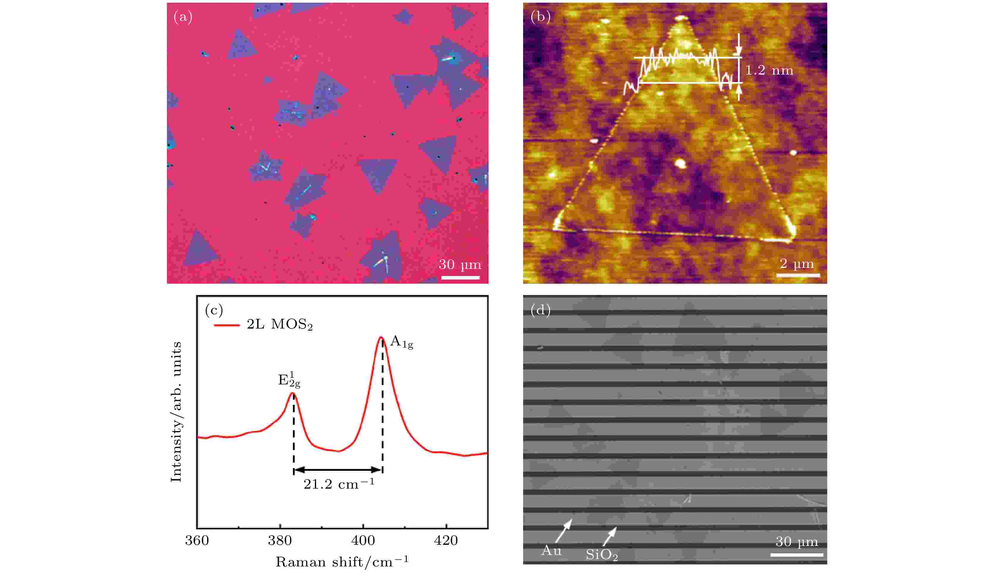
Combining with in situ nanomechanical testing system and video module of scanning electron microscope, the nanoindentation testing is performed to study the peeling-tearing behavior of two-dimensional material van der Waals heterostructures. After two-dimensional MoS2 nanosheets prepared by chemical vapor deposition are assembled into MoS2/SiO2 heterostructures by wet transfer, the nanoindentation is carried out by manipulating the tungsten probe in the in situ nanomechanical testing system. When the tungsten probe is tightly indenting into MoS2 nanosheets, a new W/MoS2/SiO2 heterostructure is assembled. With the tungsten probe retracting, the adhesive effect makes the two-dimensional MoS2 nanosheet peel off from SiO2/Si substrate to form a bulge. After reaching a certain height, under the van der Waals adhesion interaction, an incomplete penetration fracture occurs along the arc line contacting the needle. Then cleavage appears and produces two strip cracks and MoS2/SiO2 interface separation takes place simultaneously, before a large area of MoS2 nanosheet is teared. Based on the density functional theory calculation of interface binding energy density of van der Waals heterogeneous interface, the interface binding energy density of MoS2/W is verified to be larger than that of MoS2/SiO2, which explains the adhesion peeling behavior of MoS2 induced by van der Waals force between heterogeneous interfaces, perfectly. By using the peeling height and tearing length of MoS2 recorded by video module, the fracture strength of MoS2 is obtained to be 27.055 GPa and stress-strain relation can be achieved according to the film tearing model. The density functional theory simulation results show that the fracture strength of MoS2 is in a range of 21.7–32.5 GPa, and the stress-strain relation is consistent with the experimental result measured based on film tearing model. The present work is expected to play an important role in measuring the fracture strengths of two-dimensional materials, the assembly, disassembly manipulation and reliability design of two-dimensional materials and van der Waals heterostructures devices.
2022, 71 (19): 194701.
doi: 10.7498/aps.71.20220851
Abstract +
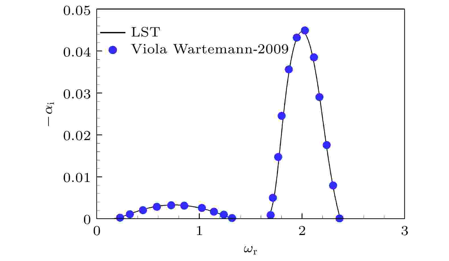
Aiming at delaying boundary-layer transition of hypersonic vehicles, the second-mode wave in the boundary layer of a Mach 6 flat plate is studied. Linear stability theory (LST) and direct numerical simulations (DNS) are used to investigate the discrete modes and the relation between the suppressing effect of second-mode wave and the location of transverse rectangular micro-groove (0.4 mm in width), respectively. The LST results show that vortex/entropy waves cause the branch types of Mack’s second mode and “mode I” modes (usually derived from fast acoustic waves) to change. The DNS results show that the influence of the grooved surface on the base flow depends on the streamwise location (or boundary-layer thickness). As the grooved surface shifts backward (or thickness increases), the influence of intensity on the base flow decreases, and the friction resistance coefficient $ C{d_{\text{f}}} $ , differential pressure resistance coefficient $ C{d_{\text{p}}} $ and total resistance coefficient $ C{d_x} $ of the grooved surface also decrease. It is found that the grooves located in front of the synchronization region of the fast mode and slow mode still have an inhibitory effect on the second-mode wave, which is different from the effect of small-sized (micrometer scale) micro-pores reported in the literature. It is also found that the suppression effect on the second-mode wave is best when the grooves are arranged in the vicinity of the maximum growth-rate point or at the location of the synchronization interval of the fast mode and slow mode.

2022, 71 (19): 194702.
doi: 10.7498/aps.71.20220352
Abstract +
Rayleigh number (Ra) dependence in Rayleigh-Bénard (RB) convection has been studied by many investigators, but the reported power-law scaling expressions are different in these researches. Previous studies have found that when Ra reaches a critical value, the flow patterns change and a transition appears in the scaling of Nu(Ra) (where Nu represents Nusselt number) and Re(Ra) (where Re denotes Reynold number). The Grossmann-Lohse(GL) model divides the Ra-Pr(where Pr refers to Prandtl number) phase into several regions to predict the scaling expressions of Nu(Ra,Pr) and Re(Ra,Pr), indicating that the thermal dissipation behavior and kinetic dissipation behaviors are diverse in the different regions. Moreover, some physical quantities also show a transition and some structures in the flow fields, such as large scale circulation and boundary layer, change when Ra increases. In this work, we conduct a series of numerical simulations in two-dimensional RB convection with Ra ranging from 107 to 1012 and Pr ranging from 0.25 to 100, which is unprecedentedly wide. The relationship between the maximum velocity and Ra is investigated, and an unexpected drop happens when Ra reaches a critical value Rac, and Rac increases with Pr increasing. The Re number, which is defined as a maximum velocity, also shows a plateau at Rac. Before and after Rac, the Ra scaling exponent of Re remains 0.55, which gets smaller at very high Ra. Specially, under different Pr values, the plateau appears at Rec ≈ 1.4 × 10⁴. In addition, a scaling Rac~Pr1.5 is found and the Ra is compensated for by Pr–1.5 to disscuss the relationship between Re and RaPr–1.5. It is interesting that the Re(RaPr–1.5) expressons at different Pr values well coincide, indicating a self-similarity of Re(RaPr–1.5). The plateau appears at RaPr–1.5 = 1 × 10⁹, meaning that Rec would reach 1.4 × 10⁴ at any Pr value when RaPr–1.5 = 1 × 10⁹. To further investigate the plateau of Re, the flow patterns are compared with time-averaged velocity fields and we find that the large scale circulation (LSC) changes from ellipse to circle at Rac. In other words, the flow pattern will change into circular LSC at Rec at different Pr values, and Rec is a constant as mentioned above. This finding can help us to distinguish the two flow patterns with given Ra and Pr, and to predict the Re scaling in an appropriate range of Ra with different Pr values.

2022, 71 (19): 194703.
doi: 10.7498/aps.71.20221128
Abstract +
As a kind of nanoscale magnetic structure, the magnetic vortex has the advantages of small size, easy integration, easy control, low driving current density, low heat loss, etc. Owing to its potential application value and research significance, it has received more and more attention since its discovery.The existence of the magnetic vortex is the result of the competition between the exchange energy and the magnetostatic energy in the system. The magnetization of magnetic vortex usually contains the in-plane part and the central region part, so it usually has dual properties of chirality and polarity. The chirality is related to the arrangement of the magnetization in the plane, which can be divided into clockwise direction and counterclockwise direction. Moreover, the polarities +1 and –1 respectively represent the magnetization in the central area of the magnetic vortex core along the +z axis and –z axis. On the one hand, the magnetic vortex can be used as an information carrier in the storage device by driving the polarity reversal, and has the advantages of fast reading and writing speed, easy erasing and rewriting. On the other hand, it is expected to be used in next-generation spintronic devices, such as spin nano-oscillators based on magnetic vortex, which can continuously output high-frequency microwave signals. To further enhance the applicability of magnetic vortex, the Dzyaloshinskii–Moriya interaction (DMI) is introduced into the system, with symmetry breaking or strong spin-orbit coupling, and its dynamic process can be regulated by changing the magnetic vortex structure. The DM effective field plays a role in forcing the adjacent magnetization to be along the perpendicular direction in the heterostructure system lacking interface inversion symmetry. Thus, the existence of DMI can make the in-plane magnetization oriented to the out-of-plane direction. In this work, the triangle-shape magnetic vortex structure is varied by changing the strength of DM effective field. The microwave magnetic fields are respectively applied along the in-plane direction and out-of-plane direction, and the eigenfrequencies are obtained by using fast Fourier transform. Next, we further explore the spin wave modes at different eigenfrequencies. Finally, we vary the intensity of DMI in the system to adjust different eigenfrequencies. These results open up possibilities for the development and application of magnetic vortex in spintronics.
PHYSICS OF GASES, PLASMAS, AND ELECTRIC DISCHARGES
EDITOR'S SUGGESTION
2022, 71 (19): 195201.
doi: 10.7498/aps.71.20220489
Abstract +
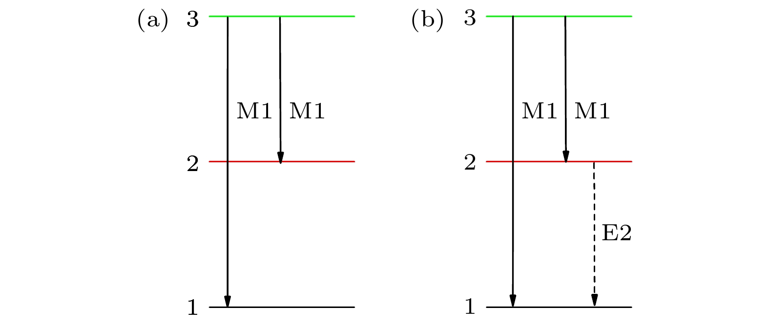
The effects of electric-quadrupole (E2) transitions on ion energy-level populations in plasma are studied by constructing the collisional radiative model of a three-level atomic system in the steady-state approximation. It is found that the influence is non-negligible at the low electron density, and becomes larger when the E2 transition rate grows with atomic number increasing. Furthermore, we investigate the E2-transition effects on the populations of levels in the ground configuration for Fe-like Mo16+ and U66+ ions in an electron-beam ion-trap plasma. The level populations are obtained by solving the large-scale rate equation numerically. On this basis, we discuss the influence of the E2 transition on the line intensity ratio of the magnetic dipole (M1) lines. In addition, we point out the significance of the E2 transitions on the intensity ratio of the M1 lines that can be used to diagnose the electron density of plasma.

EDITOR'S SUGGESTION
2022, 71 (19): 195202.
doi: 10.7498/aps.71.20220919
Abstract +
A new method for material dynamic density measurement based on proton photography is developed at XGIII facility. The protons produced by the picosecond laser of XGIII was used as the proton source to diagnose the density distribution of lattice foam under the compression of the nanosecond beam of XGIII. The density of lattice foam was calculated from the photographic results using Monte Carlo simulation method. Benefitting fromn this newly developed method, the images of the compressed lattice foam and the shock front at 5.2 ns is obtained successfully. The density distribution of the lattice foam was obtained from the images and the density of lattice foam increases about 20 times at the shock front due to the compression of the shock. The velocity of shock wave in lattice foam is also given, about 40 km/s. The density and spatial resolution of the method are further calibrated by using diamond step objects, and experimental results show that they are better than 4% and 12 μm, respectively. In order to further improve the density and spatial resolution of the proton photography at XGIII facility, a new radiogrphy method utilizing quasimonoenergetic proton beams obtained from an energy selector is proposed in this paper, and the resolution of this method is simulated by Monte Carlo program. The simulation results show that the relative density resolution can be improved to more than 1%. Through the above experimental and the simulation results, we demonstrated that diagnostic capability has been established for fast process (nanosecond scale), high pressure (nearly 100 GPa) conditions at XGIII facility.
2022, 71 (19): 195203.
doi: 10.7498/aps.71.20220720
Abstract +
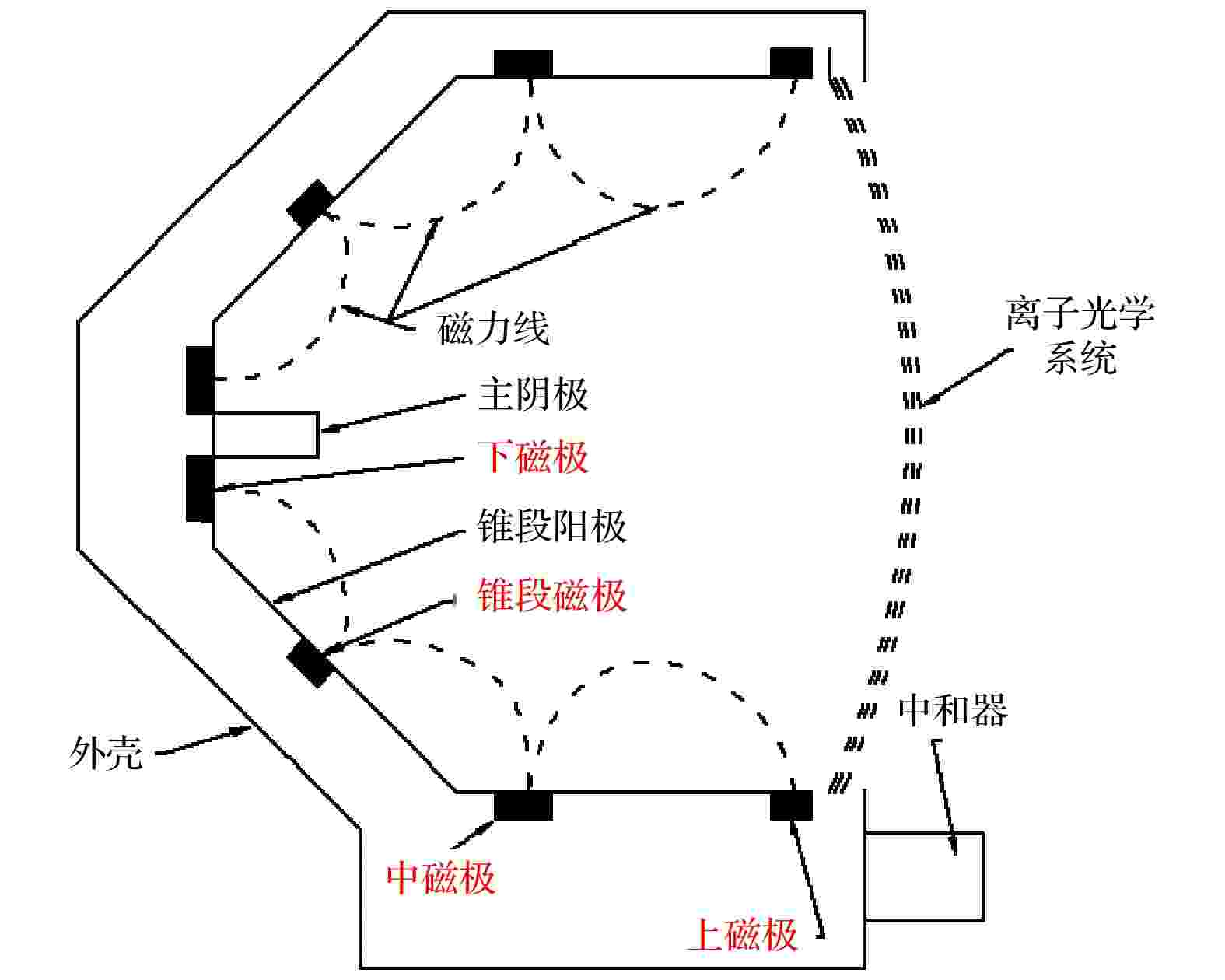
In view of the application requirements of electric propulsion system for China’s asteroid deep space exploration mission, the overall scheme is designed, an ion thruster prototype model is established by using a four-ring-cusp field discharge chamber, 30-cm beam current extraction diameter three-grid ion optics system. Reasonableness and compatibility of discharge chamber and grid design are verified experimentally and theoretically . The test results are shown below. The ion thruster can operate steadily over an input power envelope of 277–3120 W, thrust increases linearly from 9.9 to 117.2 mN, specific impulse rises from 1269 to 3492 s, the beam divergence angle drops from 30.7° to 26.8° and stabilizes above a certain power value, the thrust vector angle is less than 1.5° and beam flatness parameter is greater than 0.75 at different operating points. The maximum percentage reduction in grid gap aberration is 90% with the strain relief molybdenum mounting ring thermal design. This research provides a reference for multi-mode ion thruster design and in-orbit engineering applications.
CONDENSED MATTER: STRUCTURAL, MECHANICAL, AND THERMAL PROPERTIES
EDITOR'S SUGGESTION
2022, 71 (19): 196101.
doi: 10.7498/aps.71.20220685
Abstract +
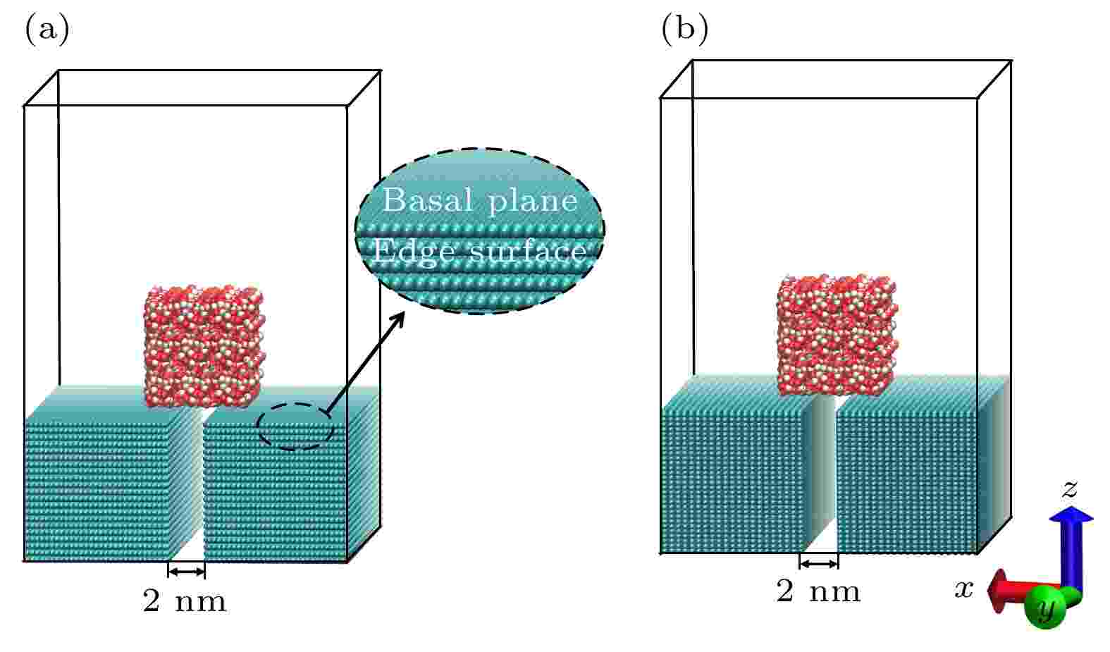
The infiltration of water droplets in nanochannels is of great importance in microfluidics. In this paper, two types of graphene nanochannels with different wall structures are constructed based on the experimentally reported graphene structure, and the infiltrations of water nanodroplet in the two nanochannels are investigated by performing all-atom molecular dynamics simulation. It is found that the two nanochannels with the same size, composed of different graphene arrays, exhibit completely different infiltration properties: water droplets cannot infiltrate into the multilayer stacked channels, but can wet the vertical array channels spontaneously and completely. By analyzing the structures of the two nanochannels, the novel phenomenon is mainly attributed to the difference in wettability between the inner surface and the outer surface of the nanochannel. From the perspective of energy, the potential energy of water droplets in the multilayer stacked channels is higher than that outside the channels, while the potential energy of water droplets in the vertical array channels is lower than that outside the channels. Therefore, water droplets can spontaneously infiltrate into the latter ones. The van der Waals interaction between the droplet and the channels and the Coulomb interaction inside the droplet play a dominant role in spontaneously infiltrating the water droplets, while the van der Waals interaction inside the droplet has little effect on the infiltration behavior. In addition, through a series of simulations of water droplets wetting the nanochannels with identical inner surface and outer surface, the wettability phase diagram of water droplets infiltration into nanochannels is established, which represents the general law of water droplet infiltration into nanochannels.

2022, 71 (19): 196201.
doi: 10.7498/aps.71.20212340
Abstract +
Silicon-based optoelectronics, using the mature silicon-based microelectronic complementary metal oxide semiconductor (CMOS) manufacturing process, is a large-scale optoelectronic integration platform that has attracted much attention. Surface plasmonic devices have also received extensive attention in the past decades, and especially the silicon-based surface plasmonic nanofocusing devices have become a research hotspot. Typical nanofocusing structures include chirped surface gratings, plasmonic Fresnel zone plate, nano-slit array, tapered metal tips. However, there occur some inevitable problems in these devices, such as the fine structure being too complex to be fabricated and too large transmission loss of metal slot waveguide. In this work, an ultra-compact hybrid surface plasmon nanofocusing device is designed and fabricated by the silicon-based optoelectronic technology, and the nanofocusing performance of the device is also experimentally verified. The hybrid surface plasmon nanofocusing devices are fabricated on a silicon-on-insulator (SOI) wafer by electron beam lithography (EBL) system. The silicon wire waveguides, tapers and the thin silicon strips in the middle of nanofocusing regions are patterned in only one step EBL. The gold layer is formed by a deposition and lift-off process, and then a partially etching process is introduced to make the thickness of the middle thin silicon strips the same as that of the gold layer. With a 1.23-μm-long tapered structure, our nanofocusing devices focus the light field of a silicon strip waveguide into a hybrid surface plasmon waveguide, making non-resonant optical field increase 20 times in the 1550 nm near-infrared band experimentally. The entire insertion loss is about 4.6 dB, and the mode area of the nanofocusing area is about ${\left( {\lambda /n} \right)^2}/640$ which is over 300 times smaller than that of the input silicon waveguide. When the middle slot silicon waveguide width WSi = 120 nm, the insertion loss reaches a minimum value of 2.8 dB. In our design, we adopt the design of silicon-based hybrid plasmonic waveguides. In this design, a layer of material with low refractive index is inserted between the metal layer and the silicon layer to act as a “container” of light field, which makes this silicon-based hybrid plasmonic waveguides have less loss than the traditional metal plasmonic waveguides, and can still maintain high optical field localization. Such silicon-based hybrid surface plasmon nanofocusing devices with simple structures and excellent performances are promising alternatives for future applications in optical field manipulation, optical sensing, nonlinear optical devices, and optical phase-change storage.
2022, 71 (19): 196801.
doi: 10.7498/aps.71.20220845
Abstract +
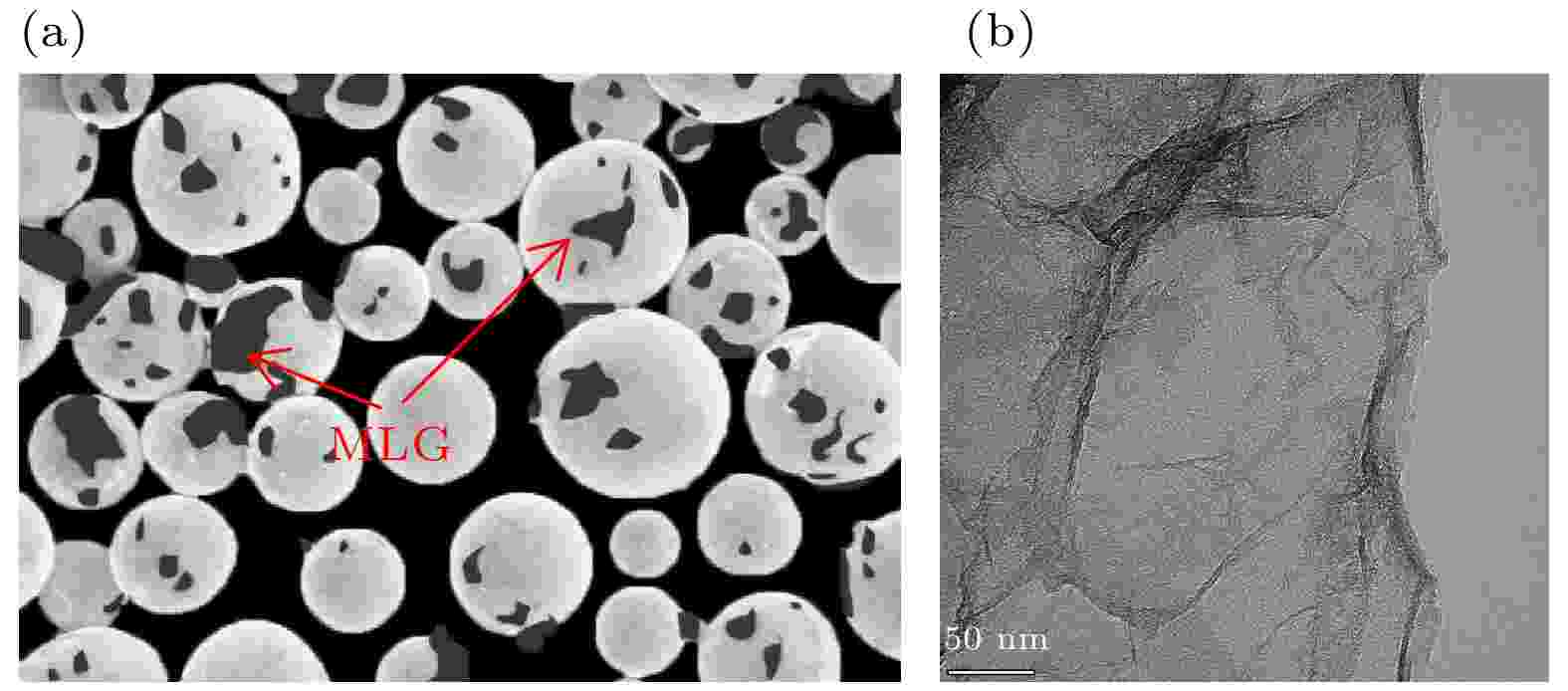
Ti2AlC and Ti3AlC formed by the reaction between C and TiAl alloy can improve the plasticity and strength of TiAl alloy respectively. Generally, the peritectic reaction of L + TiC→Ti2AlC (Ti3AlC) occurs in the process of liquid-phase sintering, but different formation mechanisms of Ti2AlC and Ti3AlC may exist in the solid-state sintering. In this work, multilayer graphene is employed to fabricate the reaction interface with TiAl alloy under 1100–1350 ℃, which is the common solid-state sintering temperature of TiAl alloy. According to the microstructure characterization and analysis, Ti2AlC and Ti3AlC are verified to contain no TiC. The interface energy values of TiC/TiAl, Ti2AlC/TiAl and Ti3AlC/TiAl are calculated to be about 1.2, 0.87 and 0.39 J·m2, respectively, indicating that Ti2AlC and Ti3AlC can be formed directly without TiC mesophase. Besides, only Ti2AlC is observed to be formed at 1150–1250 ℃, while the interface products at 1250–1350 ℃ change into Ti3AlC with a small amount of Ti2AlC. The mechanism that the sintering temperature affects the formation tendency of Ti2AlC and Ti3AlC can be ascribed to the content of α phase. The TiAl alloy matrix is composed of γ and a few α phases at 1150–1250℃, but almost completely transforms into α phase at 1250–1350 ℃, and the increase in the α content can promote the formation of Ti3AlC. The above results demonstrate the possibility of regulating the relative content of Ti2AlC and Ti3AlC through controlling the sintering temperature, which provides a promising method to improve the plasticity and strength of TiAl alloy.
CONDENSED MATTER: ELECTRONIC STRUCTURE, ELECTRICAL, MAGNETIC, AND OPTICAL PROPERTIES

COVER ARTICLE
2022, 71 (19): 197301.
doi: 10.7498/aps.71.20220834
Abstract +
EDITOR'S SUGGESTION
2022, 71 (19): 197501.
doi: 10.7498/aps.71.20220712
Abstract +
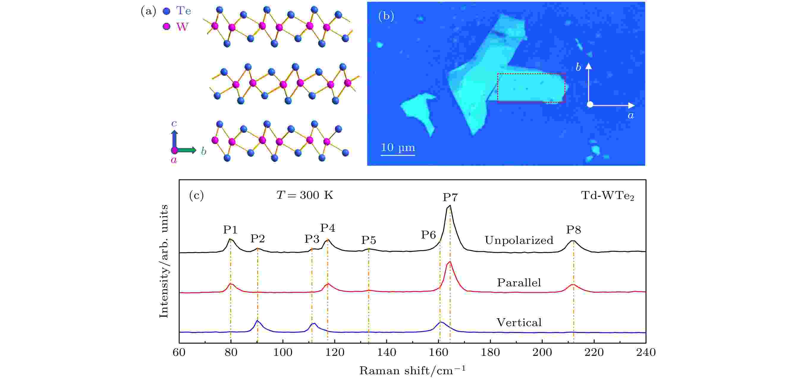
Weyl semimetal Td-phase WTe2, a novel topological matter, possesses a strong spin-orbit coupling and non-trivial topological band structure, and thus becomes a very promising superior spin current source material. By constructing the WTe2/Ti heterostructures, the issue that the ferromagnetic layer with perpendicular magnetic anisotropy cannot be directly prepared on WTe2 layer can be well addressed, and meet the requirements for high-performance spin-orbit torque devices. To be compatible with the semiconductor technology, the device integration usually involves a high temperature process. Therefore, the thermal stability of WTe2/Ti is critical for practical device fabrication and performance. However, the thermal stability of WTe2/Ti interface has not been very clear yet. In this work, the micro-Raman scattering technique is used to systematically study the WTe2/Ti interface annealed at different temperatures. It is found that the thermal stability of the interface between WTe2 and Ti is related to the thickness of WTe2 flake; appropriate increase of the WTe2 thickness can lead to the improvement of thermal stability in WTe2/Ti heterostructures. In addition, high temperature annealing can cause a significant interfacial reaction. After annealed at 473 K for 30 min, the interface between WTe2 (12 nm) and Ti changes dramatically, leading to the formation of Ti-Te interface layer. This observation is highly consistent with the observations by high-resolution transmission electron microscopy and the elemental analysis results as well. This study will provide useful information for further exploring the influence of the WTe2/Ti interface on the spin-orbit torque effect, and greatly invigorate the research area of energy efficient spintronic devices based on WTe2 and other novel topological materials.
2022, 71 (19): 197502.
doi: 10.7498/aps.71.20220745
Abstract +
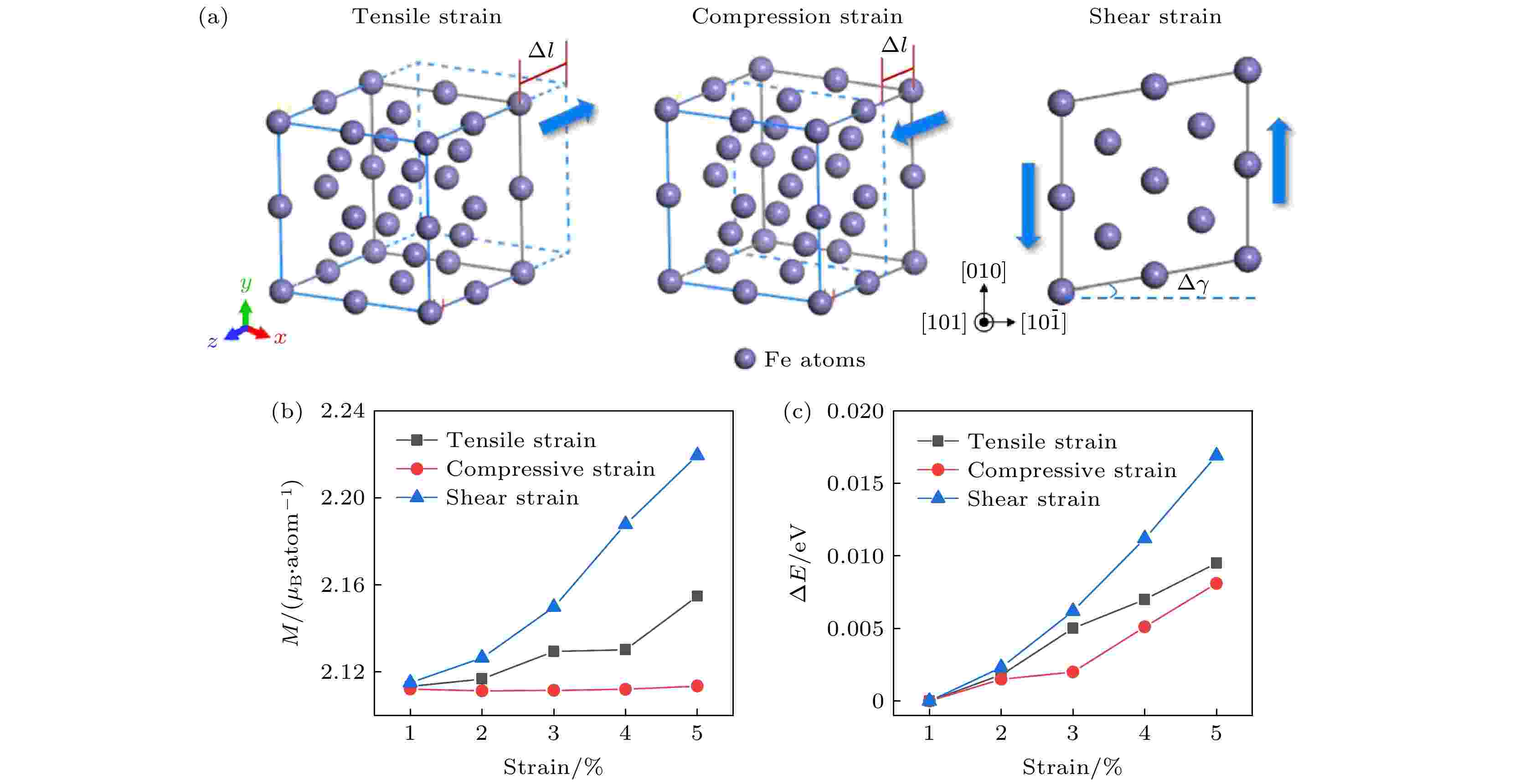
Magnetic non-destructive testing technology is widely used to detect stresses and defects in ferromagnetic materials based on the magneto-mechanical coupling effect. In the existing studies, calculated are the magnetic moment variations of the α-Fe system under axial tension and compression by using first-principles study, and the magneto-mechanical coupling mechanism is preliminarily discussed at an atomic level for the magnetic testing technology. In this work, taking the more complex doping systems Fe-C and Fe-Mn for examples, under different loading conditions of tension, compression and shearing, the coupling mechanisms such as the magnetic moment changes in different types of atomic doping systems are discussed in detail. The results show that the α-Fe and doping systems follow different changing laws of magnetic moments and energy under different types of strains. The detailed analyses of the density of states, the band structure, and the atomic magnetic moment show that doping elements change the morphology of band structure and the peak value of density of states by affecting the magnetic moment of Fe atoms, which leads the changing laws of magnetic moment and energy to be different from each other. In this work, discussed are the magneto-mechanical effects on the atomic level for ferromagnetic materials with different loading types, different doping elements and different element content. The results can be used as an important part of the multi-field coupling mechanism for magnetic testing technology.

2022, 71 (19): 197701.
doi: 10.7498/aps.71.20220654
Abstract +
Ferroelectricity and nanostructure in low-dimensional material are a research hotspot in the condensed matter physics and material science, The low-dimensional material is significant for the application and desig of nano-electronic devices. Based on the density functional theory, the In2Se3 monolayer, whose two-dimensional ferroelectricity has already been confirmed in experiment, is selected, and the ferroelectricity in the doped film and its nanoribbons are investigated. It is found that the ferroelectricity and the conductivity can coexist in the doped monolayer, and the electron doping enhances both the in-plane polarization (PIP) and the out-of-plane polarization (POOP), while the PIP is enhanced and POOP is depressed in the case of hole doping. The mechanism of the variation of polarization in the doped film is discussed on the basis of atomic distortions and electronic structures. As the In2Se3 nanoribbons are concerned, the one-dimensional ferroelectricity can be found in the In2Se3 nanowire, and the local polarization distribution within In2Se3 nanoribbons and its band gap are calculated and discussed. Furthermore, the scaling law between the band gap and the width of nanoribbon is obtained by fitting the numerical results. It is expected that our study can broaden the application scope of 2D ferroelectric films and its nanostructures.
2022, 71 (19): 197901.
doi: 10.7498/aps.71.20220544
Abstract +
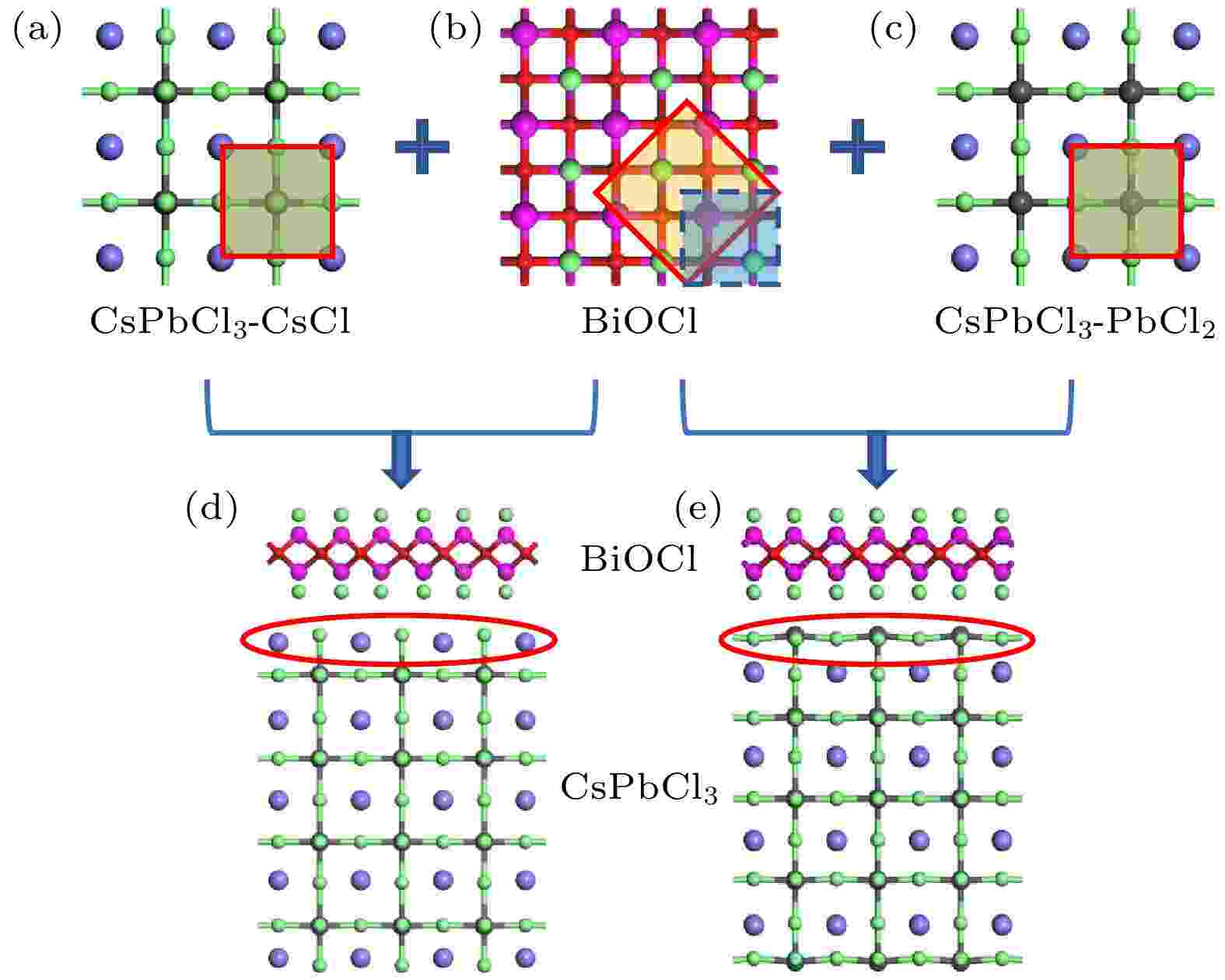
All-inorganic metal halide perovskites represented by cesium lead chloride have become important candidates for the development of high-performance photovoltaic and optoelectronic devices due to their excellent optoelectronic properties and defect tolerance. However, poor structural stability has become a bottleneck for its commercial applications. In this work, we propose to integrate thin layers of bismuth oxychloride (BiOCl) on the surface of cesium lead chloride perovskite (CsPbCl3) to form a van der Waals heterojunction. And we systematically study the environmental stability of BiOCl/CsPbCl3 van der Waals heterojunction and the influence of interfacial effects on its optoelectronic properties by combining first-principles calculations and ab initio molecular dynamics simulations. The calculated results show that the van der Waals integrated BiOCl on the surface of CsPbCl3 can greatly improve its environmental stability, which is due to the highly stable BiOCl layer isolating the reaction of water and oxygen molecules with the perovskite lattice. Moreover, the two BiOCl/CsPbCl3 van der Waals heterojunctions show a type-II band structure, which conduces to promoting the carrier separation. At the same time, the two heterojunctions have small effective carrier mass, which well preserves the excellent carrier transport properties of CsPbCl3 and BiOCl. However, CsCl-terminated heterojunctions exhibit larger band orders than PbCl2-terminated heterojunctions, which can lead to higher open-circuit voltages and lower dark currents in CsCl-terminated heterojunctions. Owing to the different band gaps of BiOCl and CsPbCl3, the heterojunctions show high optical absorption coefficients in the visible-to-ultraviolet region. This work provides a new idea and theoretical basis for improving the structural stability of CsPbCl3 perovskite materials and their applications in high-performance optoelectronic devices.
INTERDISCIPLINARY PHYSICS AND RELATED AREAS OF SCIENCE AND TECHNOLOGY
2022, 71 (19): 198101.
doi: 10.7498/aps.71.20220715
Abstract +
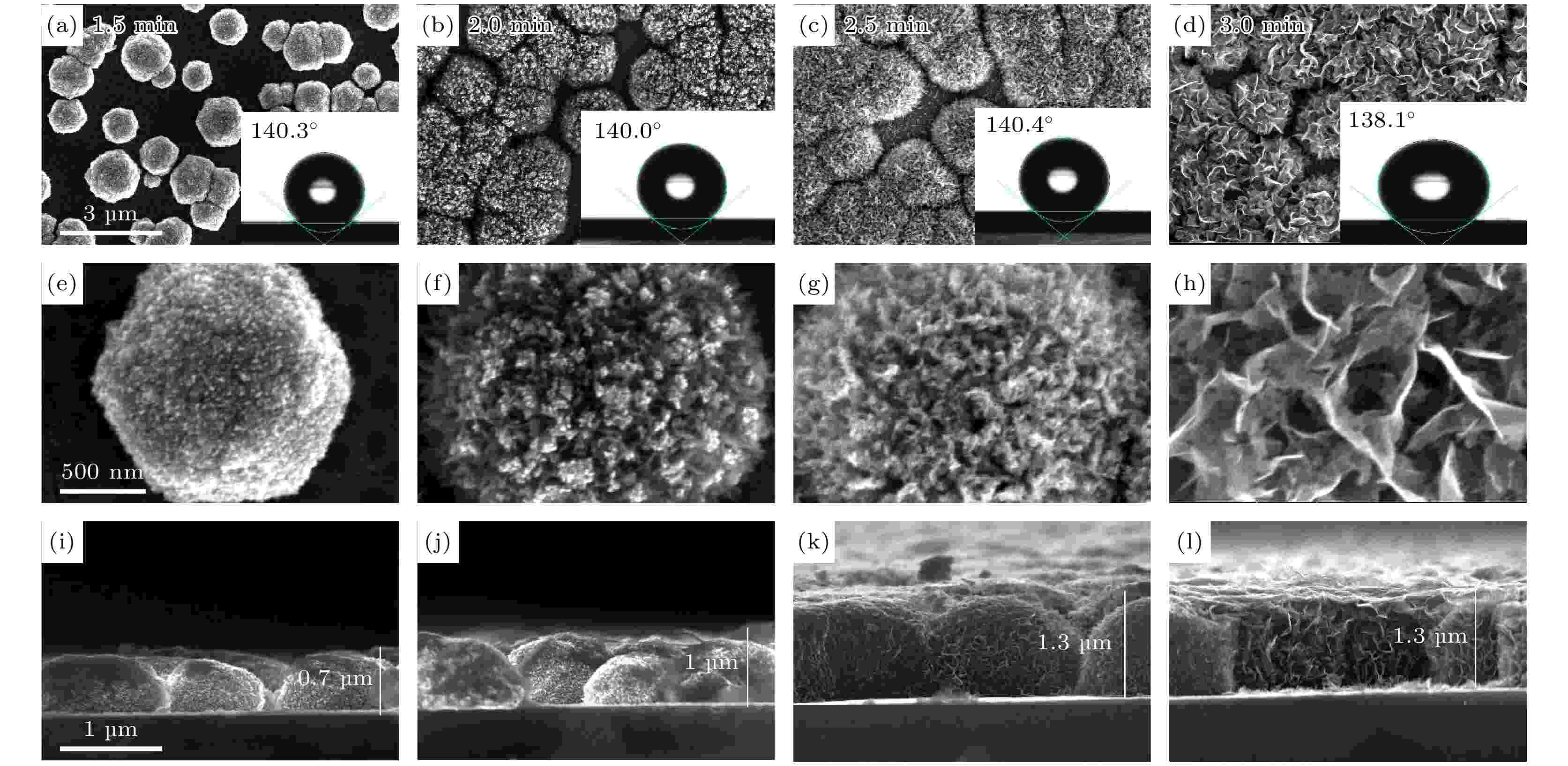
Diamond/graphene composite three-dimensional electrode has attracted extensive attention because of its low background current, wide potential window from diamond component, and high electrochemical activity from graphite component. In this work, by using the hot wire chemical vapor deposition method, nano diamonds are embedded in the vertical graphene sheet on the surface of single particle layer of nano diamond by regulating the short-term growth time to form a composite three-dimensional electrode. The results show that the electrode exhibits a wide potential window (3.59 V) and a very low background current (1.27 mA/cm2) when nano-diamond crystals grow on the top of the vertical graphene sheet. The composite structure of nano-diamond crystals coated with graphite on the top of the graphene sheet is the key to broadening the potential window and reducing the background current. With the increase of growth time, the vertical graphene sheet grows and nano-diamond grains are embedded into the lamellae, and a novel nano-diamond/graphene composite vertical lamellae structure is constructed. The ordered graphite structure increases the electrochemical active area to 677.19 μC/cm2 and the specific capacitance to 627.34 μF/cm2. The increase of graphite components makes the potential window narrow, and the embedded nano-diamond crystals effectively reduce the background current. This study provides a new method for preparing three-dimensional nanodiamond/graphene composite electrodes by hot wire chemical vapor deposition, and provides a new idea for fully exploiting the synergistic effect of diamond/graphene composite films.

2022, 71 (19): 198102.
doi: 10.7498/aps.71.20220510
Abstract +
The III-V compound semiconductor, GaN, has become an excellent semiconductor material for developing the high-frequency and high-power electronic devices because of its excellent characteristics, including large band width, high thermal conductivity and fast electron saturation rate, and has received extensive attention in recent years. However, the decomposition temperature of GaN is lower than the melting temperature, some of its fundamental properties, such as melting temperature and high temperature phase transition pressure, are still unclear, and so, now the investigation of fundamental properties dominates the whole process of this material from development to mature applications. In the present work, the classical molecular dynamics simulations combined with the first-principles calculations and lattice dynamics methods are adopted to predict the phase diagrams of GaN with wurtzite and rocksalt structures in a pressure range of 0–80 GPa. The phase transition pressures, 44.3 GPa and 45.9 GPa, obtained from the first-principles calculations and molecular dynamics simulations from wurtzite to rocksalt structure in GaN at zero temperature, are in agreement with the available experimental results (Sadovyi B, et al. 2020 Phys. Rev. B 102 235109 ). The melting temperature at 0 GPa is 2295 K obtained by extrapolating the GaN melting curve of the wurtzite structure. With the pressure increasing to 33.3 GPa, the melting curve of wurtzite structure in GaN intersects with the melting curve of rocksalt structure, and the melting temperatures of both structures increase with pressure increasing. It is found that GaN may have a superionic phase and the superionic phase transition occurs in the wurtzite structure at pressures greater than 2.0 GPa and temperatures above 2550 K, whereas the rocksalt structure undergoes a superionic phase transition at pressures and temperatures higher than 33.1 GPa and 4182 K, respectively, and both of the phase transition temperatures increase with pressure increasing. The slope of the phase boundary line of GaN is positive at high temperatures and gradually changes into a curve with a negative slope as the temperature decreases.
2022, 71 (19): 198501.
doi: 10.7498/aps.71.20220879
Abstract +
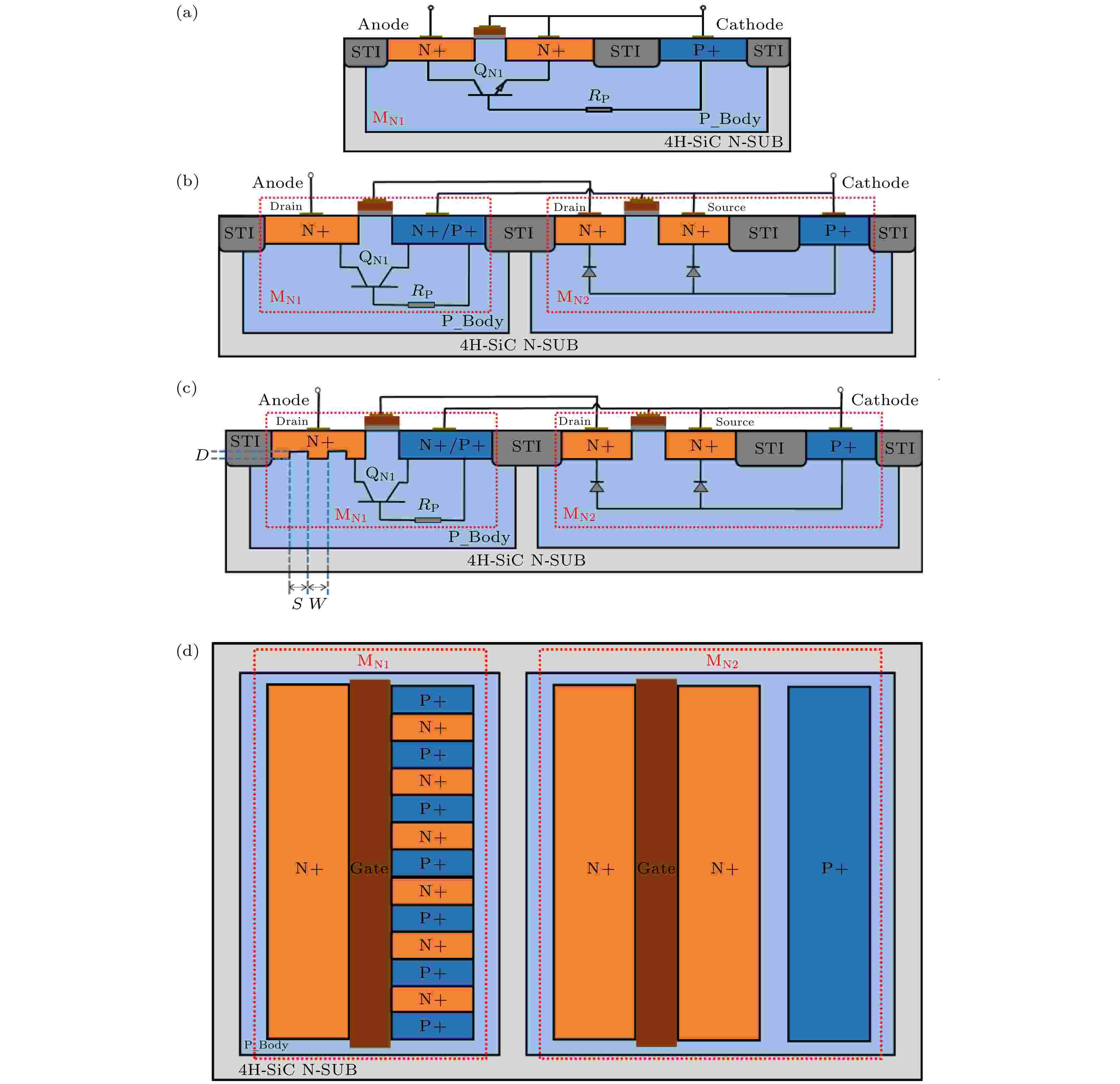
In 2020, Korean scholars proposed a new electrotatic discharge (ESD) protection device HHFGNMOS(high holding voltage floating gate nMOSFET) based on 4H-SiC material, which can significantly improve the severe snapback phenomenon of 4H-SiC GGNMOS due to the characteristics of SiC material. However, there still exists a problem that the current distribution is too dense in the HHFGNMOS structure. In this work, the comb-like structure is used for the HHFGNMOS protection device for the first time. The bottom of the drain region of the device is comb transformed, and the current distribution is made uniform by making full use of the current edge effect. The influence of design variables of comb-like structure on structure performance is given by TCAD simulation. The transient simulation results of GGNMOS, HHFGNMOS and comb-like HHFGNMOS based on 4H-SiC under TLP pulse show that the secondary failure current IT2 of comb-like HHFGNMOS increases from 17 to 22 A i.e. by 29%, compared with that of GGNMOS and HHFGNMOS. In addition, the comb-like HHFGNMOS snapback is reduced by 55.2% and 5% compared with GGNMOS snapback and HHFGNMOS snapback, respectively. Therefore, the robustness of the device is greatly improved and the snapback effect is reduced under the condition of constant area and compatible process.

2022, 71 (19): 198502.
doi: 10.7498/aps.71.20221047
Abstract +
The transistor is the core unit of digital integrated circuits, and its performance and integration are the main determinants of chip performance. With the continuous progress of nano-manufacturing technology and process, high power and heat consumption have become a major problem restricting the development of integrated circuits. Using topological insulators instead of traditional semiconductors, and the spin and valley degrees of freedom instead of charge as information carriers, to design and fabricate transistors, and the use of optical interconnections to replace metal interconnections between functional units, are effective solutions of the thermal power consumption problem of nano-integrated circuits. Based on the two-dimensional topological insulators-silicene and germanene, we theoretically propose a kind of optically controlled transistor suitable for spin bias. The effects of off-resonant circularly polarized light on the output currents of silicene and germanene transistors are calculated by using the non-equilibrium Green's function method. It is shown that the topological properties of silicene (germanene) and the output characteristics of drain current are controlled by the chirality and intensity of incident light. Under the coaction of weak left circularly polarized light and spin bias, the silicene transistors output pure spin current and fully polarized spin-up current. Under the action of strong field, the phase transition of the edge state of the silicene forms a band gap, the transistor is cut off, and the output current is almost zero. Different from the silicene transistor, the germanene transistor can obtain stable pure spin current under a weak light field, and output 100% polarized spin-down current under a strong field. By simultaneously applying off-resonant circularly polarized light of different chirality to the central device region, the germanene transistor can be turned off effectively by using the edge state phase transition induced by the polarized light field and the energy band mismatch caused by the local light field. The output poles of spin-dependent currents are almost equal for silicene and germanene transistors in the ON state, however, the breakdown voltage of the germanene transistor is significantly higher than that of the silicene transistor, and optically controlled germanene transistor can maintain effective operation at higher temperatures.
GEOPHYSICS, ASTRONOMY, AND ASTROPHYSICS
2022, 71 (19): 199601.
doi: 10.7498/aps.71.20220733
Abstract +
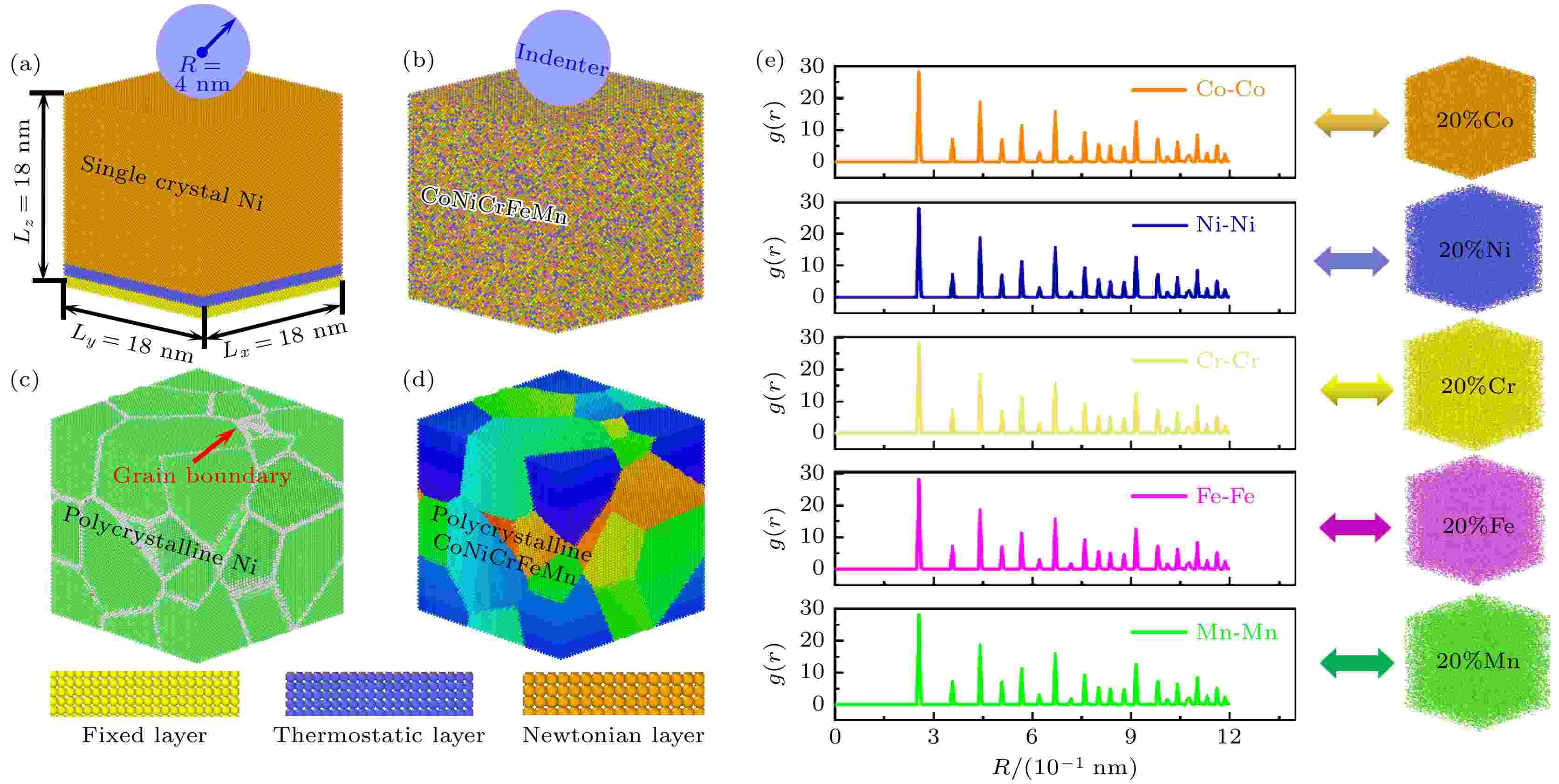
Physical property and material mechanical performance of nanocrystalline (single crystal, polycrystalline) CoNiCrFeMn alloy can be known well through an in-depth understanding of the micro-evaluation behaviour of micro dislocation, so that it can better be used in defense fields, such as nuclear reactor cladding tubes, aircraft engines, jet turbine blades and others. In this paper we propose to study the correlation between micro-structure evolution and mechanical properties for nanocrystalline CoNiCrFeMn high entropy alloy. The force driven material deformation behaviors and mechanical properties of nanocrystalline alloy and Ni material are studied by using the nanoindentation method, and effects of temperature on the mechanical properties and micro-structure evolution are compared as well. Research results show that the mechanical properties (maximum load, hardness, Young’s modulus and contact stiffness) of single crystal alloy are superior to those of single crystal Ni, which mainly stems from the fact that the single crystal high entropy alloy with a drum-shape structure is produced under loading period, and the slip and expansion of dislocations in the bulge structure are blocked. At a low temperature (5 K), the maximum load, hardness, Young's modulus and contact stiffness of polycrystalline Ni decrease by 28.9%, 20.27%, 32.61% and 36.4% respectively in comparison with those of single crystal Ni. The maximum load, hardness, Young's modulus and contact stiffness of polycrystalline CoNiCrFeMn material decrease by 21.74%, 23.61%, 23.79% and 22.90% respectively with respect to those of single CoNiCrFeMn high entropy alloy. In addition, the mechanical properties of polycrystalline alloy are more sensitive to temperature than those of single crystal high entropy alloy, whose mechanical properties decrease approximately linearly with temperature increasing. For polycrystalline CoNiCrFeMn and Ni material, the grain boundary is not merely the origin region of dislocation breeding, expansion and reproduction, but also the concentration region of defect initiation, crack expansion and failure. Its mechanical properties are weaker than those of single crystal materials due to micro-structure evolution of grain boundaries driven from stress concentration and defects existence.


