


-
氧化镓(Ga2O3)作为超宽禁带半导体在深紫外探测领域有极其重要的应用价值. 它能与GaSe形成典型的Ⅱ型异质结构, 促进载流子分离与传输, 进而实现高性能的自供电探测. 本文利用等离子体增强化学气相沉积(PECVD)技术在蓝宝石衬底上生长了Ga2O3薄膜, 并采用布里奇曼技术在氧化镓薄膜上生长了GaSe薄膜, 构建了GaSe/β-Ga2O3异质结光电探测器, 分析其中涉及的光物理与界面物理问题. 该探测器对深紫外光有很好的响应性能, 在8 V的电压下器件的暗电流仅为1.83 pA, 254 nm光照下的光电流达到了6.5 nA, 且UV-C/可见光(254 nm/600 nm)的抑制比约为354, 即使在很小的光照强度下, 响应度和探测度也达到了1.49 mA/W 和 6.65× 10¹¹ Jones. 同时, 由于结界面上的空间电荷区形成的光伏效应, 该探测器在零偏压下表现出自供电性能, 开路电压为0.2 V. 此外, 探测器有很好的灵敏度, 无论是在电压恒定的条件下用不同光强的光照射探测器, 还是在光强恒定条件下改变电压, 器件都能快速响应.UV photodetectors have the advantages of high sensitivity and fast response speed. As an ultra-wide bandgap semiconductor, gallium oxide (Ga2O3) plays an extremely important role in detecting deep ultraviolet. It can form a typical type-II heterostructure with GaSe, promoting carrier separation and transport. In this work, Ga2O3 epitaxial films are grown on sapphire substrates by plasma-assisted chemical vapor deposition (PECVD). The GaSe films and GaSe/β-Ga2O3 heterojunction photodetectors are grown on gallium oxide films by Bridgeman technology. The detector has a good response to deep ultraviolet light, the dark current of the device is only 1.83 pA at 8 V, and the photocurrent reaches 6.5 nA at 254 nm. The UVC/Visible (254 nm/600 nm) has a high rejection ratio of about 354. At very small light intensities, the responsivity and detection can reach 1.49 mA/W and 6.65 × 10¹¹ Jones, respectively. At the same time, due to the photovoltaic effect formed by the space charge region at the junction interface, the detector exhibits self-powered supply performance at zero bias voltage, and the open-circuit voltage is 0.2 V. In addition, the detector has a very good sensitivity. The device can respond quickly, whether it is irradiated with different light intensities under constant voltage, or with different voltages under constant light intensity. It can respond within milliseconds under a bias voltage of 10 V. This work demonstrates the enormous potential of heterojunctions in photoelectric detection by analyzing the photophysical and interface physical issues involved in heterojunction photodetectors, and provides a possibility for detecting the deep ultraviolet of gallium oxide.
-
Keywords:
- photoelectric detector /
- Ga2O3 /
- GaSe /
- self-power
[1] Xi Z Y, Liu Z, Yang L L, Tang K, Li L, Shen G H, Zhang M L, Li S, Guo Y F, Tang W H 2023 ACS Appl. Mater. Interfaces 15 40744
 Google Scholar
[2] Lee S H, Kim S B, Moon Y J, Kim S M, Jung H J, Seo M S, Lee K M, Kim S K, Lee S W 2017 ACS Photon. 4 2937
Google Scholar
[3] Tang X, Li K H, Zhao Y, Sui Y, Liang H, Liu Z, Liao C H, Babatain W, Lin R, Wang C, Lu Y, Alqatari F S, Mei Z, Tang W, Li X 2021 ACS Appl. Mater. Interfaces 14 1304
[4] Wang Y H, Yang Z, Li H, Li S, Zhi Y, Yan Z, Huang X, Wei X, Tang W H, Wu Z 2020 ACS Appl. Mater. Interfaces 12 47714
Google Scholar
[5] Imura S, Mineo K, Miyakawa K, Nanba M, Ohtake H, Kubota M 2018 IEEE Sensors J. 18 3108
Google Scholar
[6] Sorifi S, Kaushik S, Sheoran H, Singh R 2022 J. Phys. D: Appl. Phys. 55 365105
Google Scholar
[7] Chen Y, Lu Y, Liao M, Tian Y, Liu Q, Gao C, Yang X, Shan C 2019 Adv. Funct. Mater. 29 1906040
Google Scholar
[8] Zhao B, Wang F, Chen H, Zheng L, Su L, Zhao D, Fang X 2017 Adv. Funct. Mater. 27 1700264
Google Scholar
[9] Ozbay E, Biyikli N, Kimukin I, Kartaloglu T, Tut T, Aytur O 2004 IEEE J. Select. Topics Quantum Electron. 10 742
Google Scholar
[10] Xu Z, Zang J, Yang X, Chen Y, Lou Q, Li K, Lin C, Zhang Z, Shan C 2021 Semicond. Sci. Technol. 36 065007
Google Scholar
[11] Liu Z, Li S, Yan Z, Liu Y, Zhi Y, Wang X, Wu Z, Li P, Tang W 2020 J. Mater. Chem. C 8 5071
Google Scholar
[12] Li L, Liao F, Hu X 2020 Superlattices Microstruct. 141 106502
Google Scholar
[13] Jing L, Ai C, Guo X, Cao J, Jing D, Luo B, Ma L 2023 Ind. Eng. Chem. Res. 62 6103
Google Scholar
[14] Moon S, Bae J, Kim J 2022 J. Mater. Chem. C 10 6281
Google Scholar
[15] Lu C, Gao L, Meng F, Zhang Q, Yang L, Liu Z, Zhu M, Chen X, Lyu X, Wang Y, Liu J, Ji A, Li P, Gu L, Cao Z, Lu N 2023 J. Appl. Phys. 133 045306
Google Scholar
[16] Han Y, Jiao S, Jing J, Chen L, Rong P, Ren S, Wang D, Gao S, Wang J 2023 Nano Res. 17 2960
Google Scholar
[17] Li X, Dong J, Idrobo J C, Puretzky A A, Rouleau C M, Geohegan D B, Ding F, Xiao K 2016 J. Am. Chem. Soc. 139 482
Google Scholar
[18] Qasrawi A F 2005 Cryst. Res. Technol. 40 610
Google Scholar
[19] Lei S, Ge L, Liu Z, Najmaei S, Shi G, You G, Lou J, Vajtai R, Ajayan P M 2013 Nano Lett. 13 2777
Google Scholar
[20] Yuan X, Tang L, Liu S, Wang P, Chen Z, Zhang C, Liu Y, Wang W, Zou Y, Liu C, Guo N, Zou J, Zhou P, Hu W, Xiu F 2015 Nano Lett. 15 3571
Google Scholar
[21] Ben Aziza Z, Henck H, Pierucci D, Silly M G, Lhuillier E, Patriarche G, Sirotti F, Eddrief M, Ouerghi A 2016 ACS Nano 10 9679
Google Scholar
[22] Parlak M, Qasrawi A F, Ercelebi C 2003 Mater. Sci. 38 1507
Google Scholar
[23] Yan Z, Li S, Liu Z, Zhi Y, Dai J, Sun X, Sun S, Guo D, Wang X, Li P, Wu Z, Li L, Tang W 2020 J. Mater. Chem. C 8 4502
Google Scholar
[24] Mudiyanselage D H, Wang D, Fu H 2022 IEEE J. Electron Devices Soc. 10 89
Google Scholar
[25] Lin R, Zheng W, Zhang D, Zhang Z, Liao Q, Yang L, Huang F 2018 ACS Appl. Mater. Interfaces 10 22419
Google Scholar
[26] Abdullah M M, Bhagavannarayana G, Wahab M A 2010 J. Cryst. Growth 312 1534
Google Scholar
[27] Jubu P R, Yam F K, Igba V M, Beh K P 2020 J. Solid State Chem. 290 121576
Google Scholar
[28] 张茂林, 马万煜, 王磊, 刘增, 杨莉莉, 李山, 唐为华, 郭宇锋 2023 物理学报 72 160201
Google Scholar
Zhang M L, Ma W Y, Wang L, Liu Z, Yang L L, Li S, Tang W H, Guo Y F 2023 Acta Phys. Sin. 72 160201
Google Scholar
[29] Li Z, Xu Y, Zhang J, Cheng Y, Chen D, Feng Q, Xu S, Zhang Y, Zhang J, Hao Y, Zhang C 2019 IEEE Photon. J. 11 1
Google Scholar
[30] He T, Li C, Zhang X, Ma Y, Cao X, Shi X, Sun C, Li J, Song L, Zeng C, Zhang K, Zhang X, Zhang B 2019 Phys. Status Solidi. (a) 217 1900861
Google Scholar
[31] Yakimov E B, Polyakov A Y, Shchemerov I V, Smirnov N B, Vasilev A A, Vergeles P S, Yakimov E E, Chernykh A V, Shikoh A S, Ren F, Pearton S J 2020 APL Mater. 8 111105
Google Scholar
[32] Bae J, Park J H, Jeon D W, Kim J 2021 APL Mater. 9 101108
Google Scholar
[33] Qian L X, Liu H Y, Zhang H F, Wu Z H, Zhang W L 2019 Appl. Phys. Lett. 114 113506
Google Scholar
[34] Chen M, Zhang Z, Lv Z, Zhan R, Chen H, Jiang H, Chen J 2022 ACS Appl. Nano Mater. 5 351
Google Scholar
[35] Ricci F, Boschi F, Baraldi A, Filippetti A, Higashiwaki M, Kuramata A, Fiorentini V, Fornari R 2016 J. Phys. : Condens. Matter 28 224005
Google Scholar
[36] Filippo E, Tepore M, Baldassarre F, Siciliano T, Micocci G, Quarta G, Calcagnile L, Tepore A 2015 Appl. Surf. Sci. 338 69
Google Scholar
[37] Kong W Y, Wu G A, Wang K Y, Zhang T F, Zou Y F, Wang D D, Luo L B 2016 Adv. Mater. 28 10725
Google Scholar
[38] Liang S J, Cheng B, Cui X, Miao F 2019 Adv. Mater. 32 1903800
Google Scholar
[39] Kumar N, Kumail M, Lee J, Park H G, Kim J 2023 Mater. Res. Bull. 168 112466
Google Scholar
[40] Zhuo R, Wu D, Wang Y, Wu E, Jia C, Shi Z, Xu T, Tian Y, Li X 2018 J. Mater. Chem. C 6 10982
Google Scholar
[41] Ma Y, Chen T, Zhang X, Tang W, Feng B, Hu Y, Zhang L, Zhou X, Wei X, Xu K, Mudiyanselage D, Fu H, Zhang B 2022 ACS Appl. Mater. Interfaces 14 35194
Google Scholar
[42] Tan P, Zhao X, Hou X, Yu Y, Yu S, Ma X, Zhang Z, Ding M, Xu G, Hu Q, Gao N, Sun H, Mu W, Jia Z, Tao X, Long S 2021 Adv. Opt. Mater. 9 2100173
Google Scholar
[43] Park S, Park T, Park J H, Min J Y, Jung Y, Kyoung S, Kang T Y, Kim K H, Rim Y S, Hong J 2022 ACS Appl. Mater. Interfaces 14 25648
Google Scholar
[44] Wu C, Qiu L, Li S, Guo D, Li P, Wang S, Du P, Chen Z, Liu A, Wang X, Wu H, Wu F, Tang W 2021 Mater. Today Phys. 17 100335
Google Scholar
[45] Nguyen T M H, Tran M H, Bark C W 2023 ACS Appl. Electronic Mater. 5 6459
Google Scholar
[46] Wang Y, Tang Y, Li H, Yang Z, Zhang Q, He Z, Huang X, Wei X, Tang W, Huang W, Wu Z 2021 ACS Photon. 8 2256
Google Scholar
-
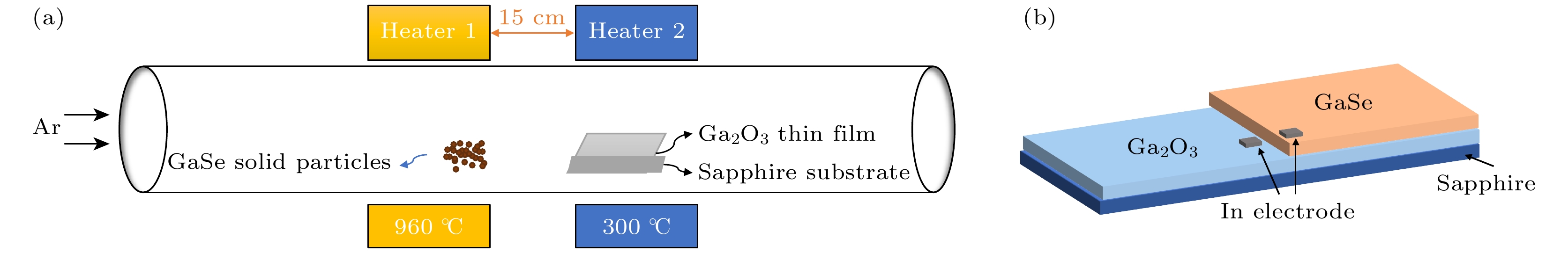
图 1 (a)实验装置示意图; (b) GaSe/β-Ga2O3异质结光电探测器示意图
Fig. 1. (a) Schematic diagram of the experimental setup; (b) schematic diagram of the GaSe/β-Ga2O3 heterojunction photodetector.
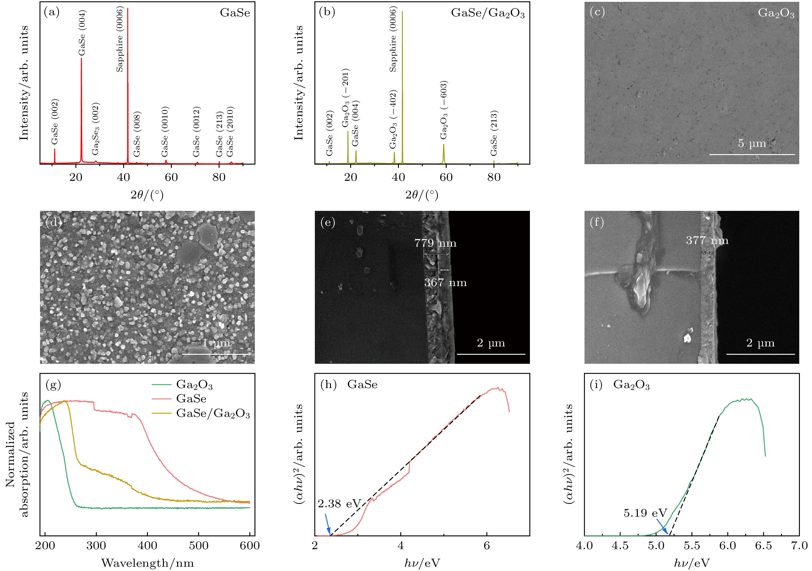
图 2 (a) GaSe薄膜XRD图; (b) Ga2O3薄膜XRD图; (c) Ga2O3薄膜表面SEM图; (d) GaSe表面SEM图; (e) Ga2O3上生长GaSe的断面SEM图; (f) 蓝宝石上生长Ga2O3而未生长GaSe的断面SEM图; (g) GaSe, β-Ga2O3薄膜和GaSe/β-Ga2O3异质结的吸收光谱曲线图; (h) GaSe薄膜的(αhυ) 2-hυ曲线图; (i) Ga2O3薄膜的(αhυ) 2-hυ曲线图
Fig. 2. (a) XRD of GaSe films; (b) XRD of Ga2O3 films; (c) SEM images of Ga2O3 films; (d) SEM images of GaSe surfaces; (e) cross-sectional SEM images of GaSe grown on Ga2O3; (f) cross-sectional SEM images of Ga2O3 grown without GaSe on sapphire; (g) absorption spectra of GaSe, β-Ga2O3 films and GaSe/β-Ga2O3 heterojunctions; (h) (αhυ)2-hυ curves of GaSe films; (i) (αhυ)2-hυ curves of Ga2O3 films.
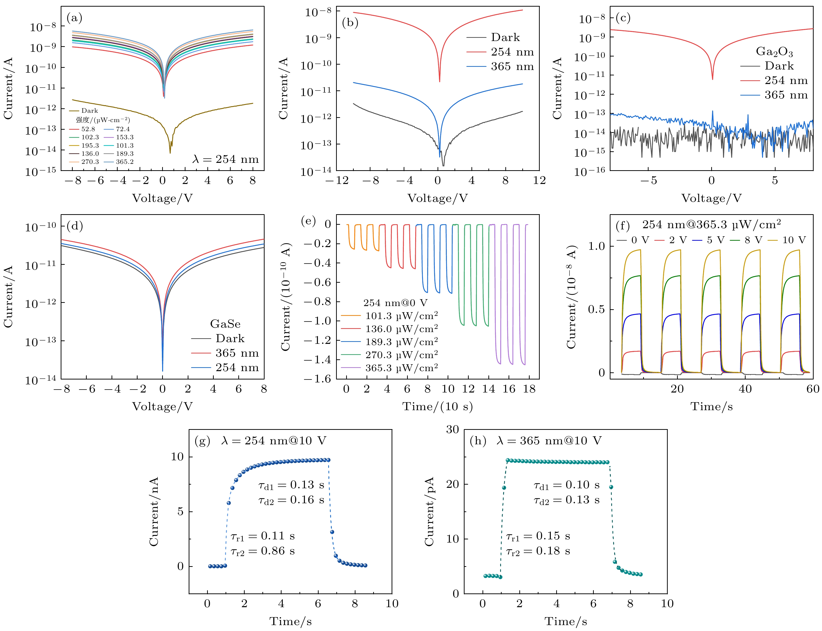
图 3 (a) 基于异质结的PD在具有不同光强度的254 nm光的黑暗和照明下的半对数I-V曲线图; (b) 光电探测器在黑暗和光照下的响应曲线图; (c) Ga2O3薄膜在黑暗和光照下的响应曲线图; (d) GaSe在黑暗和光照下的响应曲线图; (e) 0 V电压下光电探测器在不同光强的I-t曲线图; (f) 强度为365.3 μW/cm2的254 nm光照下的不同偏置电压下光开关I-t曲线图; (g) 在10 V、强度为365.3 μW/cm2的254 nm光照下拟合响应时间图; (h) 在10 V、强度为348.3 μW/cm2的365 nm光照下拟合响应时间图
Fig. 3. (a)The semi log I-V curves of the heterojunction-based PD under dark and illumination of 254 nm light with various light intensities; the semi log I-V curves under darkness and light of (b) photodetector, (c) Ga2O3 film, (d) GaSe; I-t curves with light on/off switching at (e) 0 V under various light intensities and (f) various bias voltages under 254 nm light illumination with an intensity of 365.3 μW/cm2; fitting response times under (g) 254 nm light illumination with an intensity of 365.3 μW/cm2 at 10 V, (h) 365 nm light illumination with an intensity of 348.3 μW/cm2 at 10 V.
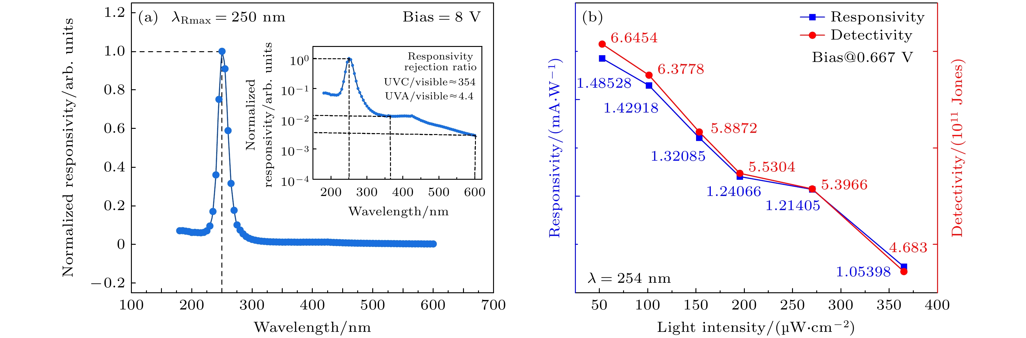
图 4 (a) GaSe/β-Ga2O3异质结光电探测器的响应光谱图; (b) 响应度和探测率与光照强度的线性关系图
Fig. 4. (a) Spectrum responsivity of the GaSe/β-Ga2O3 photodetector; (b) linear relationship between responsivity and detectivity as a function of light intensity.
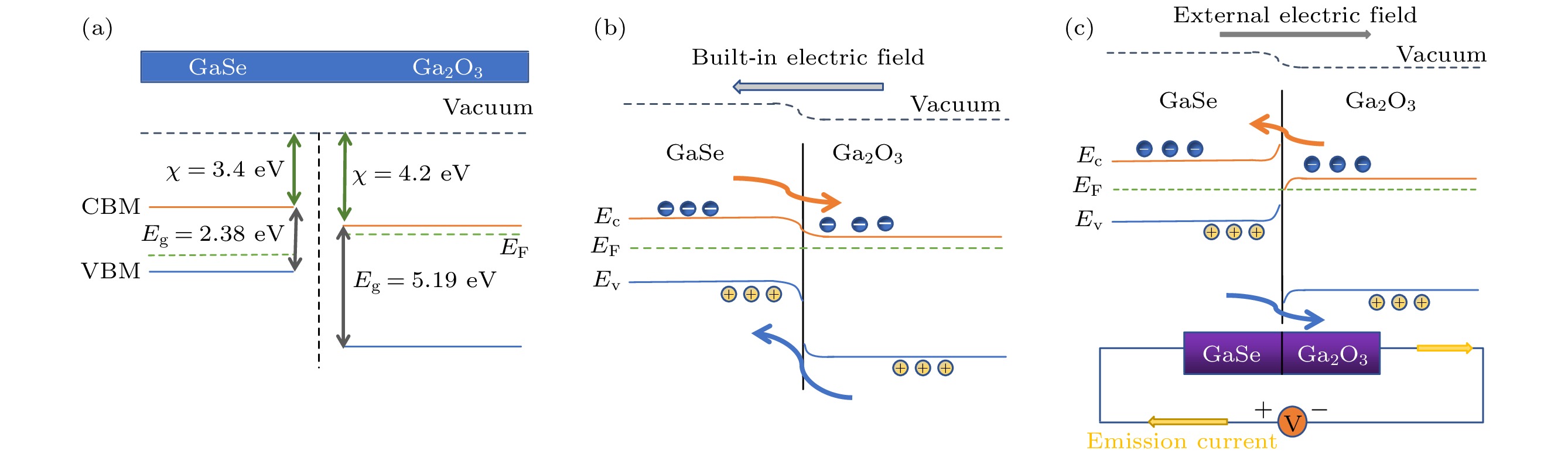
图 5 (a) GaSe和Ga2O3的能带排列图; (b) 异质结零偏压下的能带传输机制图; (c)异质结正偏压下的能带传输机制和等效电路模型图
Fig. 5. (a) Band arrangement of GaSe and Ga2O3; (b) band transport mechanism of heterojunction at zero bias; (c) band transport mechanism and equivalent circuit model of heterojunction under positive bias.
表 1 氧化镓基光电探测器性能比较
Table 1. Comparison of the performances of Ga2O3-based photodetectors
photodetector Wavelength/nm Idark/pA PDCR R/(mA·W–1) D*/Jones Reference GaSe/β-Ga2O3 254 1.83 5.5×10³ 1.49 6.65×10¹¹ This work MoS2/Ga2O3 254 0.9 670 2.05 1.2×10¹¹ [40] p-GaN/β-Ga2O3 254 3.08 4.1×10³ 3800 1.12×10¹⁴ [41] AgNW-Ga2O3 254 <10 1.2×10⁵ 14.8 5.1×10¹² [42] Ag2O/β-Ga2O3 254 92.8 3.4×10⁸ 25.65 6.1×10¹¹ [43] CuGaO2/Ga2O3 254 100 2.3×10⁴ 0.03 0.9×10¹¹ [44] CuCrO2/Ga2O3 254 18 3.5×10⁴ 0.12 4.6×10¹¹ [44] FTO/TiO2/Si-doped Ga2O3/TFB/PEDOT:PSS 254 390 242.56 1.02 0.46×10¹¹ [45]  下载: 导出CSV
-
[1] Xi Z Y, Liu Z, Yang L L, Tang K, Li L, Shen G H, Zhang M L, Li S, Guo Y F, Tang W H 2023 ACS Appl. Mater. Interfaces 15 40744
Google Scholar
[2] Lee S H, Kim S B, Moon Y J, Kim S M, Jung H J, Seo M S, Lee K M, Kim S K, Lee S W 2017 ACS Photon. 4 2937
Google Scholar
[3] Tang X, Li K H, Zhao Y, Sui Y, Liang H, Liu Z, Liao C H, Babatain W, Lin R, Wang C, Lu Y, Alqatari F S, Mei Z, Tang W, Li X 2021 ACS Appl. Mater. Interfaces 14 1304
[4] Wang Y H, Yang Z, Li H, Li S, Zhi Y, Yan Z, Huang X, Wei X, Tang W H, Wu Z 2020 ACS Appl. Mater. Interfaces 12 47714
Google Scholar
[5] Imura S, Mineo K, Miyakawa K, Nanba M, Ohtake H, Kubota M 2018 IEEE Sensors J. 18 3108
Google Scholar
[6] Sorifi S, Kaushik S, Sheoran H, Singh R 2022 J. Phys. D: Appl. Phys. 55 365105
Google Scholar
[7] Chen Y, Lu Y, Liao M, Tian Y, Liu Q, Gao C, Yang X, Shan C 2019 Adv. Funct. Mater. 29 1906040
Google Scholar
[8] Zhao B, Wang F, Chen H, Zheng L, Su L, Zhao D, Fang X 2017 Adv. Funct. Mater. 27 1700264
Google Scholar
[9] Ozbay E, Biyikli N, Kimukin I, Kartaloglu T, Tut T, Aytur O 2004 IEEE J. Select. Topics Quantum Electron. 10 742
Google Scholar
[10] Xu Z, Zang J, Yang X, Chen Y, Lou Q, Li K, Lin C, Zhang Z, Shan C 2021 Semicond. Sci. Technol. 36 065007
Google Scholar
[11] Liu Z, Li S, Yan Z, Liu Y, Zhi Y, Wang X, Wu Z, Li P, Tang W 2020 J. Mater. Chem. C 8 5071
Google Scholar
[12] Li L, Liao F, Hu X 2020 Superlattices Microstruct. 141 106502
Google Scholar
[13] Jing L, Ai C, Guo X, Cao J, Jing D, Luo B, Ma L 2023 Ind. Eng. Chem. Res. 62 6103
Google Scholar
[14] Moon S, Bae J, Kim J 2022 J. Mater. Chem. C 10 6281
Google Scholar
[15] Lu C, Gao L, Meng F, Zhang Q, Yang L, Liu Z, Zhu M, Chen X, Lyu X, Wang Y, Liu J, Ji A, Li P, Gu L, Cao Z, Lu N 2023 J. Appl. Phys. 133 045306
Google Scholar
[16] Han Y, Jiao S, Jing J, Chen L, Rong P, Ren S, Wang D, Gao S, Wang J 2023 Nano Res. 17 2960
Google Scholar
[17] Li X, Dong J, Idrobo J C, Puretzky A A, Rouleau C M, Geohegan D B, Ding F, Xiao K 2016 J. Am. Chem. Soc. 139 482
Google Scholar
[18] Qasrawi A F 2005 Cryst. Res. Technol. 40 610
Google Scholar
[19] Lei S, Ge L, Liu Z, Najmaei S, Shi G, You G, Lou J, Vajtai R, Ajayan P M 2013 Nano Lett. 13 2777
Google Scholar
[20] Yuan X, Tang L, Liu S, Wang P, Chen Z, Zhang C, Liu Y, Wang W, Zou Y, Liu C, Guo N, Zou J, Zhou P, Hu W, Xiu F 2015 Nano Lett. 15 3571
Google Scholar
[21] Ben Aziza Z, Henck H, Pierucci D, Silly M G, Lhuillier E, Patriarche G, Sirotti F, Eddrief M, Ouerghi A 2016 ACS Nano 10 9679
Google Scholar
[22] Parlak M, Qasrawi A F, Ercelebi C 2003 Mater. Sci. 38 1507
Google Scholar
[23] Yan Z, Li S, Liu Z, Zhi Y, Dai J, Sun X, Sun S, Guo D, Wang X, Li P, Wu Z, Li L, Tang W 2020 J. Mater. Chem. C 8 4502
Google Scholar
[24] Mudiyanselage D H, Wang D, Fu H 2022 IEEE J. Electron Devices Soc. 10 89
Google Scholar
[25] Lin R, Zheng W, Zhang D, Zhang Z, Liao Q, Yang L, Huang F 2018 ACS Appl. Mater. Interfaces 10 22419
Google Scholar
[26] Abdullah M M, Bhagavannarayana G, Wahab M A 2010 J. Cryst. Growth 312 1534
Google Scholar
[27] Jubu P R, Yam F K, Igba V M, Beh K P 2020 J. Solid State Chem. 290 121576
Google Scholar
[28] 张茂林, 马万煜, 王磊, 刘增, 杨莉莉, 李山, 唐为华, 郭宇锋 2023 物理学报 72 160201
Google Scholar
Zhang M L, Ma W Y, Wang L, Liu Z, Yang L L, Li S, Tang W H, Guo Y F 2023 Acta Phys. Sin. 72 160201
Google Scholar
[29] Li Z, Xu Y, Zhang J, Cheng Y, Chen D, Feng Q, Xu S, Zhang Y, Zhang J, Hao Y, Zhang C 2019 IEEE Photon. J. 11 1
Google Scholar
[30] He T, Li C, Zhang X, Ma Y, Cao X, Shi X, Sun C, Li J, Song L, Zeng C, Zhang K, Zhang X, Zhang B 2019 Phys. Status Solidi. (a) 217 1900861
Google Scholar
[31] Yakimov E B, Polyakov A Y, Shchemerov I V, Smirnov N B, Vasilev A A, Vergeles P S, Yakimov E E, Chernykh A V, Shikoh A S, Ren F, Pearton S J 2020 APL Mater. 8 111105
Google Scholar
[32] Bae J, Park J H, Jeon D W, Kim J 2021 APL Mater. 9 101108
Google Scholar
[33] Qian L X, Liu H Y, Zhang H F, Wu Z H, Zhang W L 2019 Appl. Phys. Lett. 114 113506
Google Scholar
[34] Chen M, Zhang Z, Lv Z, Zhan R, Chen H, Jiang H, Chen J 2022 ACS Appl. Nano Mater. 5 351
Google Scholar
[35] Ricci F, Boschi F, Baraldi A, Filippetti A, Higashiwaki M, Kuramata A, Fiorentini V, Fornari R 2016 J. Phys. : Condens. Matter 28 224005
Google Scholar
[36] Filippo E, Tepore M, Baldassarre F, Siciliano T, Micocci G, Quarta G, Calcagnile L, Tepore A 2015 Appl. Surf. Sci. 338 69
Google Scholar
[37] Kong W Y, Wu G A, Wang K Y, Zhang T F, Zou Y F, Wang D D, Luo L B 2016 Adv. Mater. 28 10725
Google Scholar
[38] Liang S J, Cheng B, Cui X, Miao F 2019 Adv. Mater. 32 1903800
Google Scholar
[39] Kumar N, Kumail M, Lee J, Park H G, Kim J 2023 Mater. Res. Bull. 168 112466
Google Scholar
[40] Zhuo R, Wu D, Wang Y, Wu E, Jia C, Shi Z, Xu T, Tian Y, Li X 2018 J. Mater. Chem. C 6 10982
Google Scholar
[41] Ma Y, Chen T, Zhang X, Tang W, Feng B, Hu Y, Zhang L, Zhou X, Wei X, Xu K, Mudiyanselage D, Fu H, Zhang B 2022 ACS Appl. Mater. Interfaces 14 35194
Google Scholar
[42] Tan P, Zhao X, Hou X, Yu Y, Yu S, Ma X, Zhang Z, Ding M, Xu G, Hu Q, Gao N, Sun H, Mu W, Jia Z, Tao X, Long S 2021 Adv. Opt. Mater. 9 2100173
Google Scholar
[43] Park S, Park T, Park J H, Min J Y, Jung Y, Kyoung S, Kang T Y, Kim K H, Rim Y S, Hong J 2022 ACS Appl. Mater. Interfaces 14 25648
Google Scholar
[44] Wu C, Qiu L, Li S, Guo D, Li P, Wang S, Du P, Chen Z, Liu A, Wang X, Wu H, Wu F, Tang W 2021 Mater. Today Phys. 17 100335
Google Scholar
[45] Nguyen T M H, Tran M H, Bark C W 2023 ACS Appl. Electronic Mater. 5 6459
Google Scholar
[46] Wang Y, Tang Y, Li H, Yang Z, Zhang Q, He Z, Huang X, Wei X, Tang W, Huang W, Wu Z 2021 ACS Photon. 8 2256
Google Scholar

 下载:
下载:
计量
- 文章访问数: 6890
- PDF下载量: 342
- 被引次数: 0
