


-
The static random access memory (SRAM), as a common and important high-speed storage module in modern digital circuit systems, plays an important role in improving the performances of electronic systems. The data about the total ionizing dose (TID) radiation effect of SRAM cell have not been rich in the literature so far. In this work, a novel 6-transistor SRAM cell (6T LB SRAM cell) based on L-type gate body-contact (LB) MOSFET device is designed and fabricated by 130nm silicon-on-insulator (SOI) process. The LB MOSFET follows the center-symmetric layout design of the SRAM cell, reducing the area by approximately 22% compared with the SRAM cell using the T-type gate MOSFET contact device (6T TB SRAM cell) of the same device size. The electrical performance difference between LB MOSFET and other devices is compared. Besides this, the variations of the leakage current and the reading static noise margin (RSNM) of SRAM cells based on different MOSFETs under various total ionizing doses are also investigated. The test results indicate that the LB MOS successfully suppresses the floating body effect (FBE), and that the drain-induced barrier lowing (DIBL) and drain-to-source breakdown voltage (BVds) characteristics are improved. The performance of this device is similar to that of TB MOS device, but due to the special body contact design, the former has an advantage of smaller area. Due to the use of the body contact device, the leakage current of the 6T LB SRAM cell is significantly smaller than that of the conventional floating device SRAM cell (6T FB SRAM cell), which has lower static power consumption. After 60Co-γ ray irradiation, the 700 krad(Si) radiation dose only increases the leakage current of 6T LB SRAM cell by 21.9%, which is better than 41.4% of 6T FB SRAM cell. In addition, the 6T LB SRAM cell has an RSNM value similar to that of the 6T TB SRAM cell, and this is 1.93 times higher than the that of 6T FB SRAM cell. The radiation experiment causes the butterfly curve of the 6T FB SRAM cell to be asymmetrically deformed, and the stability of the SRAM cell is deteriorated due to the TID effect. However, the test results show that when the radiation dose reaches 700 krad (Si), the RSNM value of the 6T LB SRAM cell is reduced only by 11.2%. Therefore, 6T LB SRAM cell has stable and reliable practical value.
-
Keywords:
- static random access memory cell /
- total ionizing dose effects /
- silicon-on-insulator /
- body-contact
[1] Schwank J R, Cavrois F, Shaneyfelt M R, Paillet P, Dodd P E 2003 IEEE Trans. Nucl. Sci. 50 522
 Google Scholar
[2] Verma S, Abdullah M 2015 Int. J. Computer Appl. 130 17
[3] Barnaby H J 2006 IEEE Trans. Nucl. Sci. 53 3103
Google Scholar
[4] Yao X Y, Hindman N, Clark L T, Holbert K E, Alexander D R, Shedd W M 2008 IEEE Trans. Nucl. Sci. 55 3280
Google Scholar
[5] Annamalai N K, Biwer M C 1988 IEEE Trans. Nucl. Sci. 35 1372
Google Scholar
[6] Colinge J P, Terao A 1993 IEEE Trans. Nucl. Sci. 40 78
Google Scholar
[7] Schwank J R, Shaneyfelt M R, Draper B L, Dodd P E 1999 IEEE Trans. Nucl. Sci. 46 1809
Google Scholar
[8] Parke S, DeGregorio K, Goldston M, Hayhurst R, Hackler D 2005 IEEE Aerospace Conference
[9] Mercha A, Rafi J M, Simoen E, Augendre E, Claeys C 2003 IEEE Trans. Electron Devices 50 1675
Google Scholar
[10] Chaudhry A, Kumar M J 2004 IEEE Trans. Device Mater. Reliab. 4 99
Google Scholar
[11] Kaifi M, Siddiqui M J 2011 International Conference on Multimedia, Signal Processing and Communication Technologies, Aligarh, Uttar Pradesh, India December17—19, 2011 p216
[12] Maeda S, Hirano Y, Yamaguchi Y, Iwamatsu T, Ipposhi T, Ueda K, Mashiko K, Maegawa S, Abe H, Nishimura T 1999 IEEE Trans. Electron Devices 46 151
Google Scholar
[13] Singh J, Mohanty S P, Pradhan D K 2013 Robust SRAM Designs and Analysis (New York: Springer Science+Business Media) pp31—56
[14] He W W, Chen J, Luo J X, Chai Z, Wang X 2016 Electron. Lett. 52 1172
Google Scholar
[15] Arora 1993 MOSFET Models for VLSI Circuit Simulation: Theory and Practice (Berlin: Springer) pp210—219
[16] Ning B X, Zhang Z X 2013 International Journal of Electronics and Electrical Engineering 1 31
Google Scholar
[17] Youk G U, Khare P S, Schrimpf R D, Massengill L W, Galloway K F 1999 IEEE Trans. Nucl. Sci. 46 1830
Google Scholar
[18] Peng C, Zhang Z X, Hu Z Y, Huang H X, Ning B X, Bi D W 2013 Chin. Phys. Lett. 30 098502
Google Scholar
[19] Seevinck E, List F J, Lohstroh J 1987 IEEE J. Solid-State Circuits 22 748
Google Scholar
[20] 宁冰旭 2013 博士学位论文(上海: 中国科学院上海微系统与信息技术研究所)
Ning B X 2013 Ph. D. Dissertation (Shanghai: Shanghai Institute of Microsystem and Information Technology March) (in Chinese)
[21] Re V, Manghisoni M, Ratti L, Speziali V, Traversi G 2005 IEEE Radiat. Eff. Data Workshop 122
[22] Uyemura J P 2002 Introduction to VLSI Circuits and Systems (Hoboken: Wiley) pp237—244
-
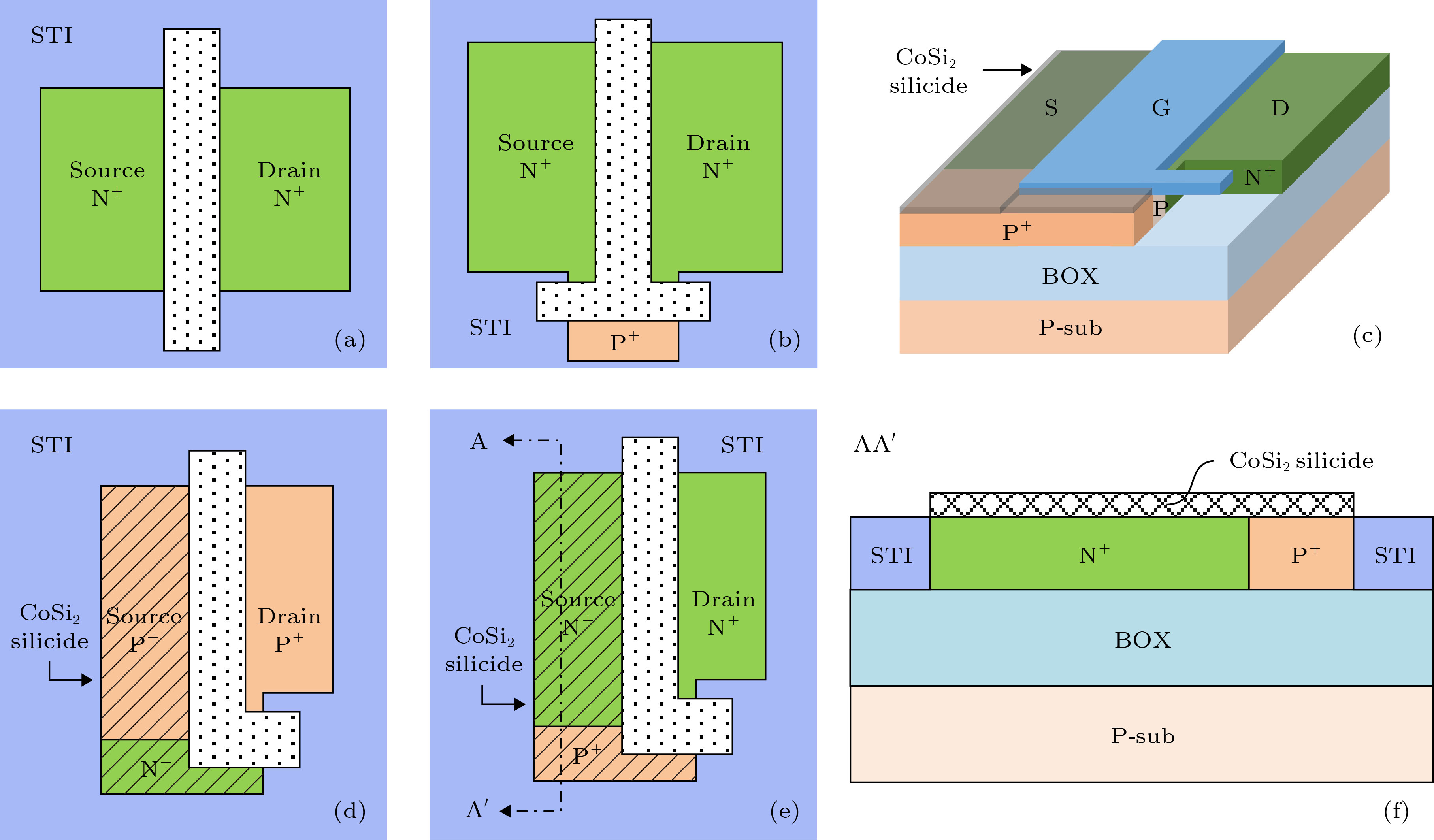
图 1 (a) FB NMOS版图; (b) TB NMOS版图; (c) LB NMOS 3维示意图; (d) LB PMOS版图; (e) LB NMOS版图; (f) LB NMOS器件沿(e)图线A-A'截取的器件横截面图
Figure 1. (a) The layout of FB SOI nMOSFET; (b) the layout of TB SOI nMOSFET; (c) the LB nMOSFET 3-dimensional schematic; (d) the layout of LB pMOSFET; (e) the layout of LB nMOSFET; (f) a cross-sectional view of LB nMOSFET is taken along line A-A' in (e).
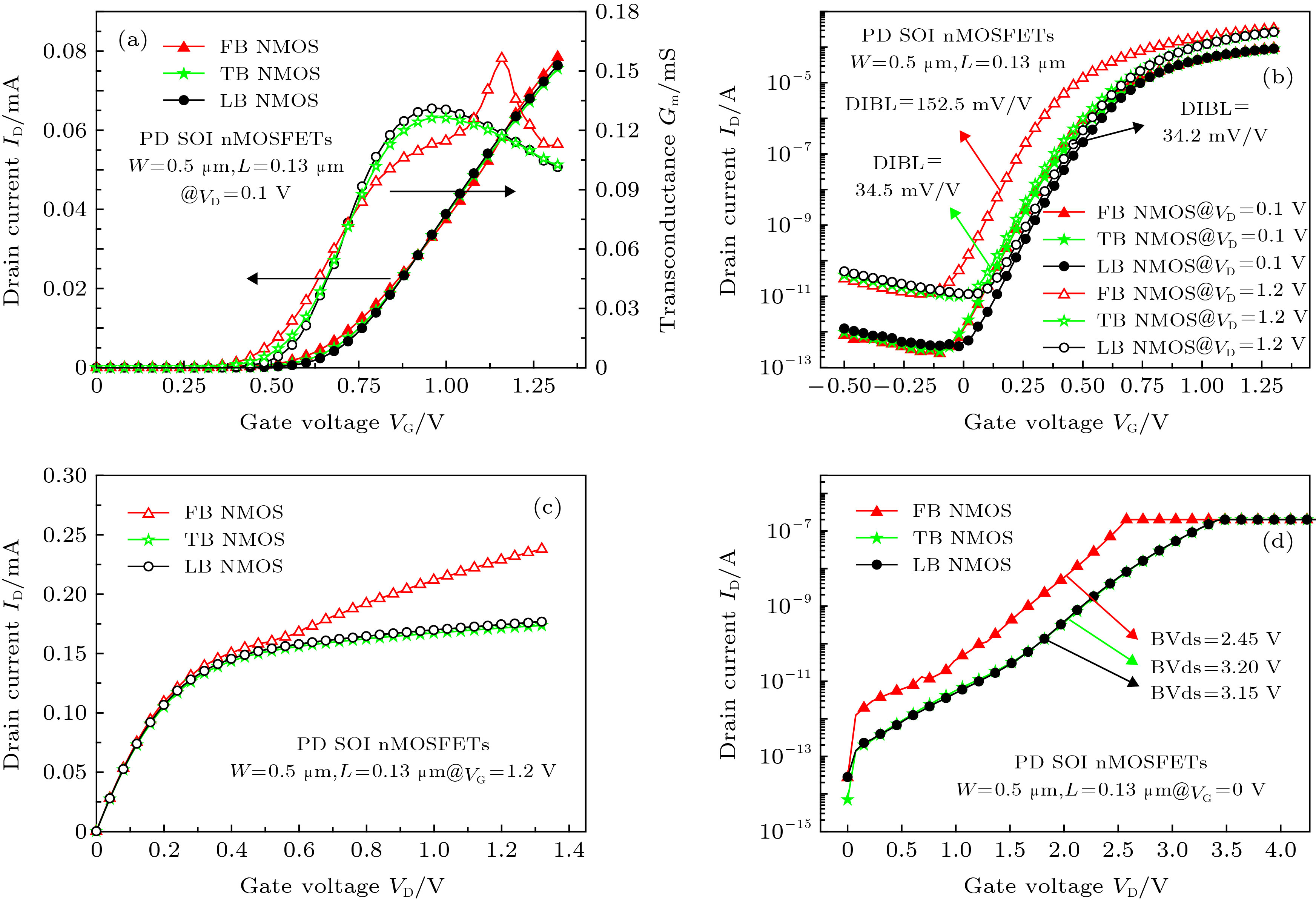
图 2 FB, TB和LB NMOS器件的 (a) 转移特性曲线和跨导; (b) ID-VG曲线; (c) 输出特性曲线; (d) BVds曲线
Figure 2. (a) Transmission characteristic curve and transconductance; (b) ID-VG curve; (c) output characteristic curve; (d) BVds curves for the FB, TB and LB NMOS devices.

图 3 (a) 基于FB器件的6管静态随机存储器单元的原理图; (b) 基于LB(或TB)器件的6管静态随机存储器单元的原理图
Figure 3. SOI SRAM cell schematic circuit of (a) The 6T FB SRAM cell; (b) the 6T LB SRAM cell or 6T TB SRAM cell.
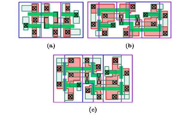
图 4 (a) 基于FB器件的6管静态随机存储器单元的版图示意图; (b) 基于LB器件的6管静态随机存储器单元的版图示意图; (c) 基于TB器件的6管静态随机存储器单元的版图示意图
Figure 4. SOI SRAM cell schematic layout of (a) The 6T FB SRAM cell; (b) the 6T LB SRAM cell; (c) the 6T TB SRAM cell.
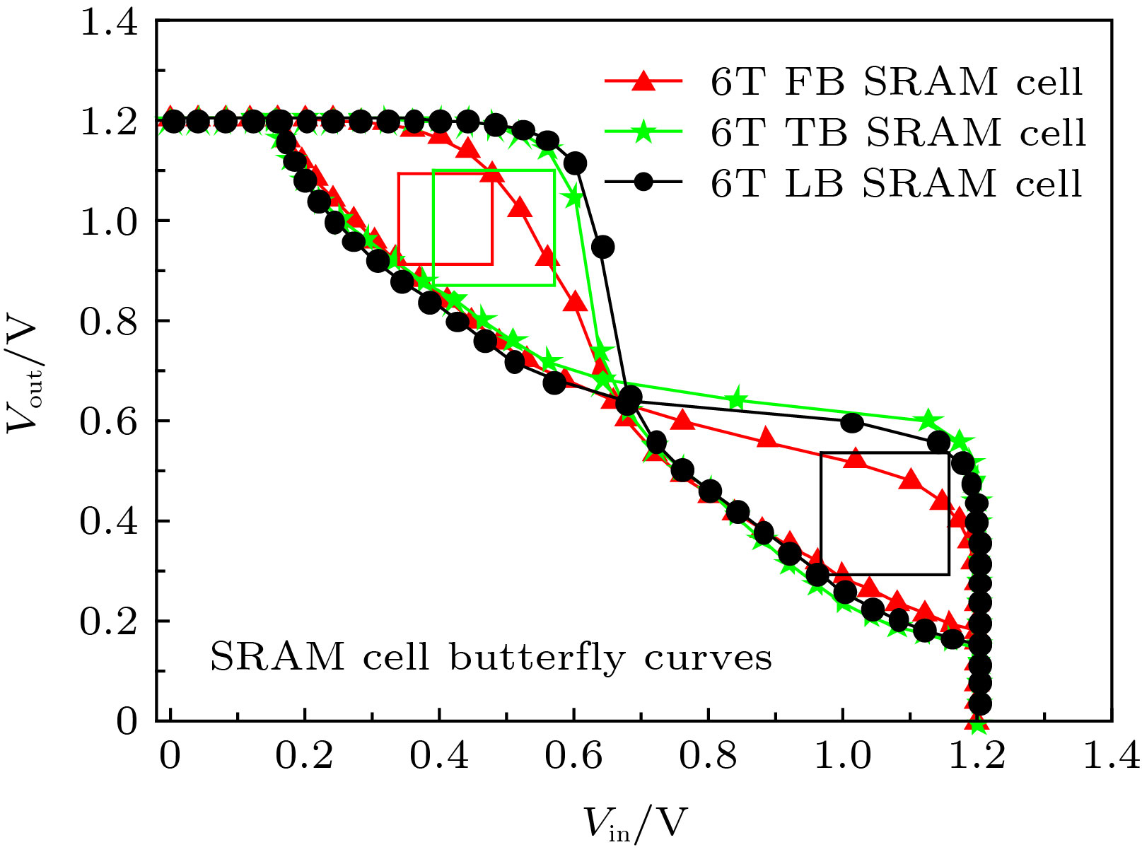
图 5 基于LB, TB和FB MOS器件的静态随机存储器单元的RSNM曲线
Figure 5. The RSNM curves of FB/TB/LB SRAM cell.
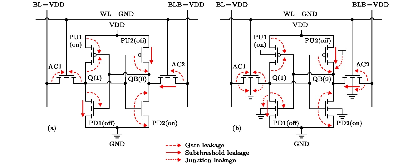
图 6 (a) 6T FB SRAM cell与 (b) 6T LB SRAM cell的漏电流测试电路及漏电路径示意图(假定Q存储1逻辑值, QB存储0逻辑值)
Figure 6. The leakage current test circuit and the leakage path diagram of (a) 6T FB SRAM cell and (b) 6T LB SRAM cell (Assuming Q stores 1 logical value and QB stores 0 logical value)
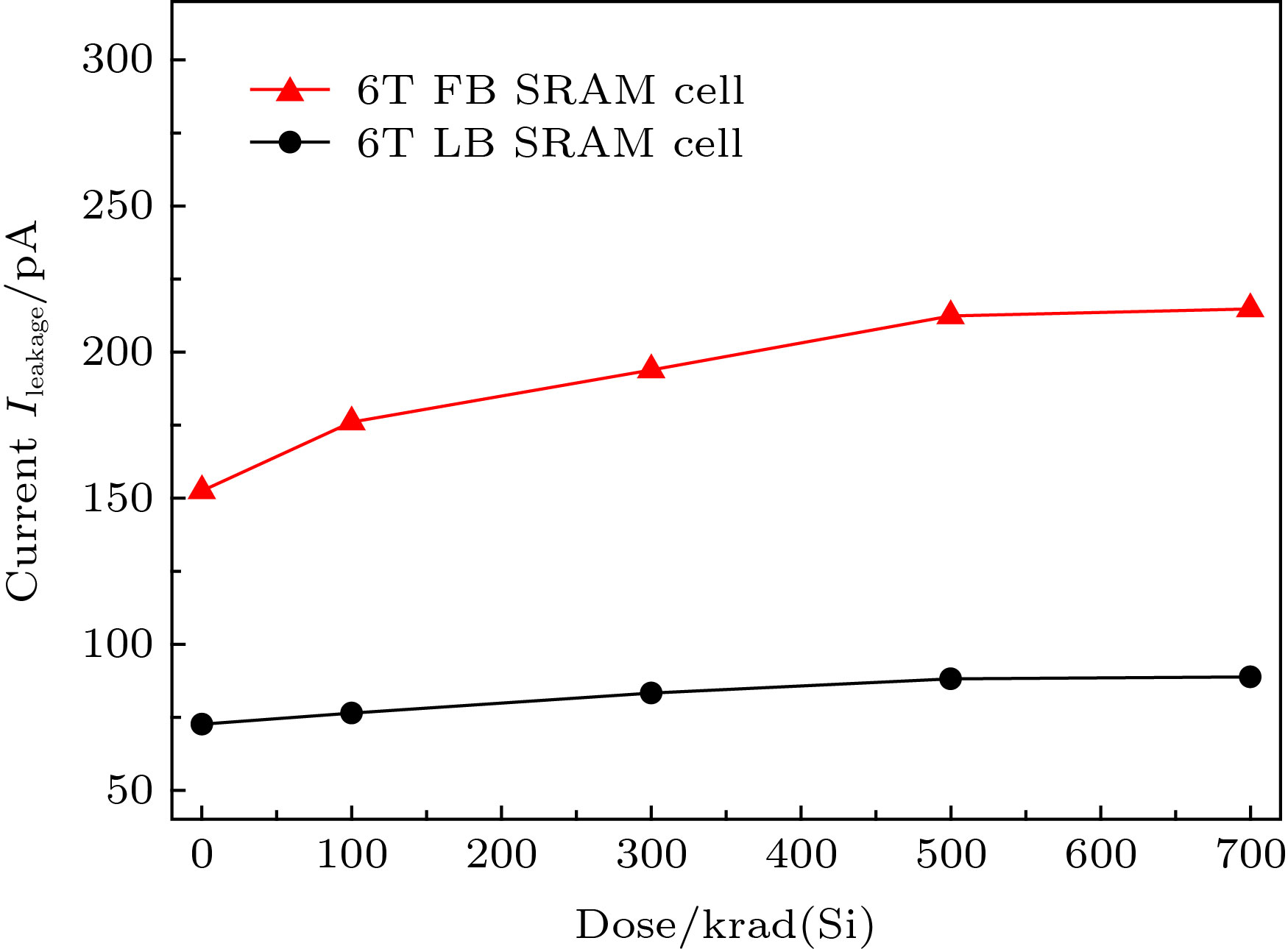
图 7 基于LB和FB MOS器件的静态随机存储器单元的漏电流在不同辐射总剂量下的变化情况
Figure 7. The cell leakage current of 6T FB SRAM cell and 6T LB SRAM cell at different radiation doses.
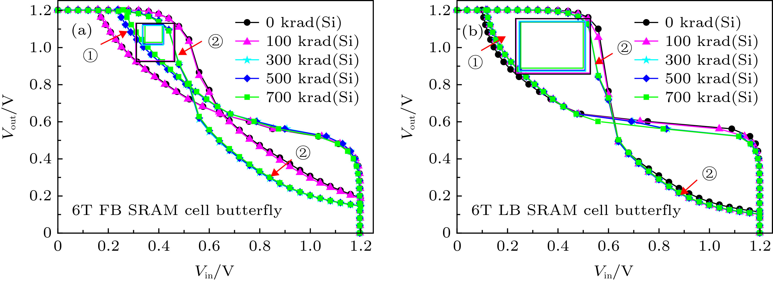
图 8 (a)基于FB MOS器件的静态随机存储器单元和(b)基于LB MOS器件的静态随机存储器单元的读取静态噪声容限受总剂量辐射的影响
Figure 8. (a) 6T FB Cell read stability and (b) 6T LB Cell read stability under various radiation doses.
表 1 基于LB和FB MOS器件静态随机存储器单元在辐照过程中的偏置条件
Table 1. Bias conditions of 6T LB cell and 6T FB cell during irradiation.
测试项 VDD GND SUB WL BL BLB Q QB 漏电流(Ileakage)/V 1.32 0 0 0 1.32 1.32 读取静态噪声容限(RSNM)/V 1.32 0 0 1.32 1.32 1.32 0 1.32  DownLoad: CSV
-
[1] Schwank J R, Cavrois F, Shaneyfelt M R, Paillet P, Dodd P E 2003 IEEE Trans. Nucl. Sci. 50 522
Google Scholar
[2] Verma S, Abdullah M 2015 Int. J. Computer Appl. 130 17
[3] Barnaby H J 2006 IEEE Trans. Nucl. Sci. 53 3103
Google Scholar
[4] Yao X Y, Hindman N, Clark L T, Holbert K E, Alexander D R, Shedd W M 2008 IEEE Trans. Nucl. Sci. 55 3280
Google Scholar
[5] Annamalai N K, Biwer M C 1988 IEEE Trans. Nucl. Sci. 35 1372
Google Scholar
[6] Colinge J P, Terao A 1993 IEEE Trans. Nucl. Sci. 40 78
Google Scholar
[7] Schwank J R, Shaneyfelt M R, Draper B L, Dodd P E 1999 IEEE Trans. Nucl. Sci. 46 1809
Google Scholar
[8] Parke S, DeGregorio K, Goldston M, Hayhurst R, Hackler D 2005 IEEE Aerospace Conference
[9] Mercha A, Rafi J M, Simoen E, Augendre E, Claeys C 2003 IEEE Trans. Electron Devices 50 1675
Google Scholar
[10] Chaudhry A, Kumar M J 2004 IEEE Trans. Device Mater. Reliab. 4 99
Google Scholar
[11] Kaifi M, Siddiqui M J 2011 International Conference on Multimedia, Signal Processing and Communication Technologies, Aligarh, Uttar Pradesh, India December17—19, 2011 p216
[12] Maeda S, Hirano Y, Yamaguchi Y, Iwamatsu T, Ipposhi T, Ueda K, Mashiko K, Maegawa S, Abe H, Nishimura T 1999 IEEE Trans. Electron Devices 46 151
Google Scholar
[13] Singh J, Mohanty S P, Pradhan D K 2013 Robust SRAM Designs and Analysis (New York: Springer Science+Business Media) pp31—56
[14] He W W, Chen J, Luo J X, Chai Z, Wang X 2016 Electron. Lett. 52 1172
Google Scholar
[15] Arora 1993 MOSFET Models for VLSI Circuit Simulation: Theory and Practice (Berlin: Springer) pp210—219
[16] Ning B X, Zhang Z X 2013 International Journal of Electronics and Electrical Engineering 1 31
Google Scholar
[17] Youk G U, Khare P S, Schrimpf R D, Massengill L W, Galloway K F 1999 IEEE Trans. Nucl. Sci. 46 1830
Google Scholar
[18] Peng C, Zhang Z X, Hu Z Y, Huang H X, Ning B X, Bi D W 2013 Chin. Phys. Lett. 30 098502
Google Scholar
[19] Seevinck E, List F J, Lohstroh J 1987 IEEE J. Solid-State Circuits 22 748
Google Scholar
[20] 宁冰旭 2013 博士学位论文(上海: 中国科学院上海微系统与信息技术研究所)
Ning B X 2013 Ph. D. Dissertation (Shanghai: Shanghai Institute of Microsystem and Information Technology March) (in Chinese)
[21] Re V, Manghisoni M, Ratti L, Speziali V, Traversi G 2005 IEEE Radiat. Eff. Data Workshop 122
[22] Uyemura J P 2002 Introduction to VLSI Circuits and Systems (Hoboken: Wiley) pp237—244

 DownLoad:
Catalog
Metrics
- Abstract views: 14136
- PDF Downloads: 82
- Cited By: 0
