-
Field effect transistors (FETs) based on two-dimensional (2D) materials have great potential applications in very large-scale integration technology, and high-performance short channel 2D semiconductor FETs are essential. Owing to the difficulty in obtaining channel lengths below 10 nm for 2D materials, there are few stable methods of fabricating short channel 2D semiconductor FETs. Here we report a method of stably fabricating vertical short-channel MoS2 FETs by using graphene as the contact material and h-BN as the spacer. The 8-nm spacer transistor exhibits good switching characteristics. The on/off ratio is greater than 107 and the off-state current is less than 100 fA/μm under different source-drain voltages, which are immune well to the direct source-to-drain tunneling effect. This method can be used to rapidly screen two-dimensional materials that are immune to short-channel effects and also are suitable for the fabrication of high-performance FETs.
-
Keywords:
- two-dimensional materials /
- MoS2 /
- field effect transistor /
- short channel effect
[1] Das S, Sebastian A, Pop E, McClellan C J, Franklin A D, Grasser T, Knobloch T, Illarionov Y, Penumatcha A V, Appenzeller J, Chen Z H, Zhu W J, Asselberghs I, Li L J, Avci U E, Bhat N, Anthopoulos T D, Singh R 2021 Nat. Electron. 4 786
 Google Scholar
[2] Sakaki H, Noda T, Hirakawa K, Tanaka M, Matsusue T 1987 Appl. Phys. Lett. 51 1934
 Google Scholar
[3] Liu Y, Duan X, Shin H J, Park S, Huang Y, Duan X 2021 Nature 591 43
 Google Scholar
[4] Uchida K, Watanabe H, Kinoshita A, Koga J, Numata T, Takagi S 2002 Experimental Study on Carrier Transport Mechanism in Ultrathin-body SOI n and p-MOSFETs with SOI Thickness Less than 5 nm (IEEE), San Francisco, CA, USA, December 8–11 2002 p47
[5] Fiori G, Bonaccorso F, Iannaccone G, Palacios T, Neumaier D, Seabaugh A, Banerjee S K, Colombo L 2014 Nat. Nanotechnol. 9 768
 Google Scholar
[6] Chhowalla M, Jena D, Zhang H 2016 Nat. Rev. Mater. 1 16052
 Google Scholar
[7] Akinwande D, Huyghebaert C, Wang C H, Serna M I, Goossens S, Li L J, Wong H P, Koppens F H L 2019 Nature 573 507
 Google Scholar
[8] Radisavljevic B, Radenovic A, Brivio J, Giacometti V, Kis A 2011 Nat. Nanotechnol. 6 147
 Google Scholar
[9] Desai S B, Madhvapathy S R, Sachid A B, Llinas J P, Wang Q, Ahn G H, Pitner G, Kim M J, Bokor J, Hu C, Wong H P, Javey A 2016 Science 354 99
 Google Scholar
[10] Nourbakhsh A, Zubair A, Huang S, Ling X, Dresselhaus M S, Kong J, De Gendt S, Palacios T 2015 2015 Symposium on VLSI Technology Digests of Technical Kyoto, Japan, June 16–18, 2015 p28
[11] Xie L, Liao M, Wang S, Yu H, Du L, Tang J, Zhao J, Zhang J, Chen P, Lu X, Wang G, Xie G, Yang R, Shi D, Zhang G 2017 Adv. Mater. 29 1702522
 Google Scholar
[12] Lingming Y, Kausik M, Yuchen D, Han L, Heng W, Hatzistergos M, Hung P Y, Robert T, Wilman T, Chris H, Peide D Y 2014 2014 Symposium on VLSI Technology Digest of Technical, Honolulu, HI, USA, June 9–12, 2014 p1
[13] Yang L, Lee R T P, Ra S S P, Tsai W, Ye P D 2015 2015 73rd Annual Device Research Conference (DRC), Columbus, OH, USA, June 21–24, 2015 p237
[14] Nourbakhsh A, Zubair A, Sajjad R N, Tavakkoli K G A, Chen W, Fang S, Ling X, Kong J, Dresselhaus M S, Kaxiras E, Berggren K K, Antoniadis D, Palacios T 2016 Nano Lett. 16 7798
 Google Scholar
[15] Xu K, Chen D, Yang F, Wang Z, Yin L, Wang F, Cheng R, Liu K, Xiong J, Liu Q, He J 2017 Nano Lett. 17 1065
 Google Scholar
[16] Liu Y, Guo J, Wu Y, Zhu E, Weiss N O, He Q, Wu H, Cheng H C, Xu Y, Shakir I, Huang Y, Duan X 2016 Nano Lett. 16 6337
 Google Scholar
[17] Cao W, Liu W, Kang J, Banerjee K 2016 IEEE Electron Device Lett. 37 1497
 Google Scholar
[18] Yang Z Y, Liu X Q, Zou X M, Wang J L, Ma C, Jiang C Z, Ho J C, Pan C F, Xiao X H, Xiong J, Liao L 2017 Adv. Funct. Mater. 27 1602250
 Google Scholar
[19] Xiao X, Chen M, Zhang J, Zhang T, Zhang L, Jin Y, Wang J, Jiang K, Fan S, Li Q 2019 ACS Appl. Mater. Inter. 11 11612
 Google Scholar
[20] Jiang J, Doan M H, Sun L, Kim H, Yu H, Joo M K, Park S H, Yang H, Duong D L, Lee Y H 2020 Adv. Sci. 7 1902964
 Google Scholar
[21] Liu Y, Guo J, Zhu E, Liao L, Lee S J, Ding M, Shakir I, Gambin V, Huang Y, Duan X 2018 Nature 557 696
 Google Scholar
[22] Kawaura H, Sakamoto T, Baba T 2000 Appl. Phys. Lett. 76 3810
 Google Scholar
[23] Kawaura H, Baba T 2003 Jpn. J. Appl. Phys. 42 351
 Google Scholar
[24] Qiu C, Liu F, Xu L, Deng B, Xiao M, Si J, Lin L, Zhang Z, Wang J, Guo H, Peng H, Peng L M 2018 Science 361 387
 Google Scholar
-
图 1 垂直沟道MoS2晶体管加工过程 (a) 机械剥离在300 nm SiO2衬底上的BN-A; (b) 干法转移后的石墨烯A/BN-A异质结; (c) RIE刻蚀后边界对齐的石墨烯A/BN-A异质结; (d) 边界对齐后石墨烯A/BN-A转移到石墨烯B上后形成的石墨烯A/BN-A/石墨烯B异质结; (e) 湿法转移MoS2到(d)上; (f) 转移BN-B到MoS2上作为顶栅介电层; (g) 沉积源漏栅极电极 (图中P++表示P型重掺杂)
Figure 1. Fabrication process of vertical channel MoS2 transistors: (a) Mechanical exfoliation of BN-A on 300 nm SiO2 substrate; (b) transfer graphene-A/BN-A heterostructure; (c) aligned graphene-A/BN-A heterostructure after RIE etching; (d) transfer graphene-A/BN-A onto graphene-B; (e) transfer monolayer MoS2 onto (d) by wet transfer process; (f) transfer BN-B onto MoS2 as the top gate dielectric; (g) deposition of source, drain and gates electrodes (P++ represents P-type heavy doping).
图 2 8 nm垂直短沟道MoS2-FET结构 (a) 垂直短沟道晶体管的结构示意图, 红色虚线方框部分为晶体管垂直沟道区域; (b) 短沟道器件光学显微镜图; (c) 间隙BN-A的原子力显微镜测量图, 间隙BN厚度约为8 nm; (d) 刻蚀后氮化硼斜面截面透射电子显微镜图, 顶切角度为38°
Figure 2. Structure of 8 nm vertical short-channel MoS2-FET: (a) Structure diagram of the vertical short-channel transistor, the red dotted box is the vertical channel region of the transistor; (b) optical microscope image of short-channel devices; (c) atomic force microscope image of spacer BN-A with a thickness is about 8 nm; (d) transmission electron microscope image of BN cross-section after etching, and the top-cut angle is 38°.
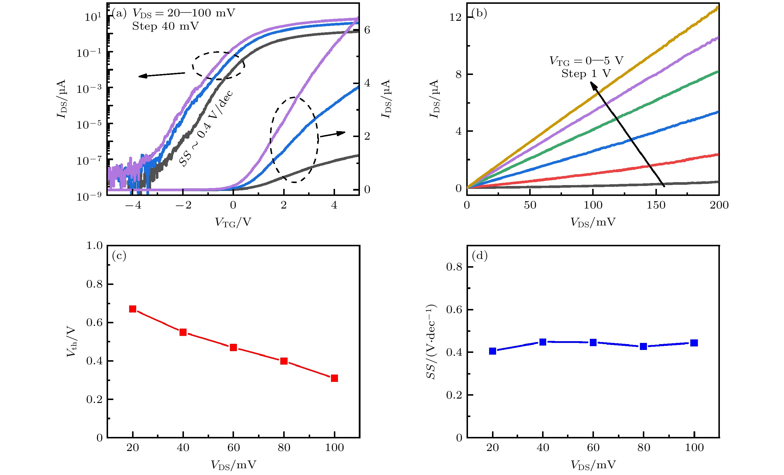
图 3 8 nm垂直沟道MoS2晶体管电学表征 (a) 不同源漏电压VDS下的转移特性曲线IDS-VGS, 亚阈值摆幅(SS) 约为0.4 V/dec; (b) 传输特性曲线IDS-VDS; (c) 晶体管阈值电压Vth随源漏电压VDS的变化; (d) 亚阈值摆幅随源漏电压VDS的变化
Figure 3. Electrical characteristics of 8 nm vertical channel MoS2 transistor: (a) Transfer characteristic curve IDS-VGS with different VDS, subthreshold swing (SS) is about 0.4 V/dec; (b) output characteristic curve IDS-VDS; (c) threshold voltage Vth as a function of VDS; (d) subthreshold swing as a function of VDS.
-
[1] Das S, Sebastian A, Pop E, McClellan C J, Franklin A D, Grasser T, Knobloch T, Illarionov Y, Penumatcha A V, Appenzeller J, Chen Z H, Zhu W J, Asselberghs I, Li L J, Avci U E, Bhat N, Anthopoulos T D, Singh R 2021 Nat. Electron. 4 786
 Google Scholar
[2] Sakaki H, Noda T, Hirakawa K, Tanaka M, Matsusue T 1987 Appl. Phys. Lett. 51 1934
 Google Scholar
[3] Liu Y, Duan X, Shin H J, Park S, Huang Y, Duan X 2021 Nature 591 43
 Google Scholar
[4] Uchida K, Watanabe H, Kinoshita A, Koga J, Numata T, Takagi S 2002 Experimental Study on Carrier Transport Mechanism in Ultrathin-body SOI n and p-MOSFETs with SOI Thickness Less than 5 nm (IEEE), San Francisco, CA, USA, December 8–11 2002 p47
[5] Fiori G, Bonaccorso F, Iannaccone G, Palacios T, Neumaier D, Seabaugh A, Banerjee S K, Colombo L 2014 Nat. Nanotechnol. 9 768
 Google Scholar
[6] Chhowalla M, Jena D, Zhang H 2016 Nat. Rev. Mater. 1 16052
 Google Scholar
[7] Akinwande D, Huyghebaert C, Wang C H, Serna M I, Goossens S, Li L J, Wong H P, Koppens F H L 2019 Nature 573 507
 Google Scholar
[8] Radisavljevic B, Radenovic A, Brivio J, Giacometti V, Kis A 2011 Nat. Nanotechnol. 6 147
 Google Scholar
[9] Desai S B, Madhvapathy S R, Sachid A B, Llinas J P, Wang Q, Ahn G H, Pitner G, Kim M J, Bokor J, Hu C, Wong H P, Javey A 2016 Science 354 99
 Google Scholar
[10] Nourbakhsh A, Zubair A, Huang S, Ling X, Dresselhaus M S, Kong J, De Gendt S, Palacios T 2015 2015 Symposium on VLSI Technology Digests of Technical Kyoto, Japan, June 16–18, 2015 p28
[11] Xie L, Liao M, Wang S, Yu H, Du L, Tang J, Zhao J, Zhang J, Chen P, Lu X, Wang G, Xie G, Yang R, Shi D, Zhang G 2017 Adv. Mater. 29 1702522
 Google Scholar
[12] Lingming Y, Kausik M, Yuchen D, Han L, Heng W, Hatzistergos M, Hung P Y, Robert T, Wilman T, Chris H, Peide D Y 2014 2014 Symposium on VLSI Technology Digest of Technical, Honolulu, HI, USA, June 9–12, 2014 p1
[13] Yang L, Lee R T P, Ra S S P, Tsai W, Ye P D 2015 2015 73rd Annual Device Research Conference (DRC), Columbus, OH, USA, June 21–24, 2015 p237
[14] Nourbakhsh A, Zubair A, Sajjad R N, Tavakkoli K G A, Chen W, Fang S, Ling X, Kong J, Dresselhaus M S, Kaxiras E, Berggren K K, Antoniadis D, Palacios T 2016 Nano Lett. 16 7798
 Google Scholar
[15] Xu K, Chen D, Yang F, Wang Z, Yin L, Wang F, Cheng R, Liu K, Xiong J, Liu Q, He J 2017 Nano Lett. 17 1065
 Google Scholar
[16] Liu Y, Guo J, Wu Y, Zhu E, Weiss N O, He Q, Wu H, Cheng H C, Xu Y, Shakir I, Huang Y, Duan X 2016 Nano Lett. 16 6337
 Google Scholar
[17] Cao W, Liu W, Kang J, Banerjee K 2016 IEEE Electron Device Lett. 37 1497
 Google Scholar
[18] Yang Z Y, Liu X Q, Zou X M, Wang J L, Ma C, Jiang C Z, Ho J C, Pan C F, Xiao X H, Xiong J, Liao L 2017 Adv. Funct. Mater. 27 1602250
 Google Scholar
[19] Xiao X, Chen M, Zhang J, Zhang T, Zhang L, Jin Y, Wang J, Jiang K, Fan S, Li Q 2019 ACS Appl. Mater. Inter. 11 11612
 Google Scholar
[20] Jiang J, Doan M H, Sun L, Kim H, Yu H, Joo M K, Park S H, Yang H, Duong D L, Lee Y H 2020 Adv. Sci. 7 1902964
 Google Scholar
[21] Liu Y, Guo J, Zhu E, Liao L, Lee S J, Ding M, Shakir I, Gambin V, Huang Y, Duan X 2018 Nature 557 696
 Google Scholar
[22] Kawaura H, Sakamoto T, Baba T 2000 Appl. Phys. Lett. 76 3810
 Google Scholar
[23] Kawaura H, Baba T 2003 Jpn. J. Appl. Phys. 42 351
 Google Scholar
[24] Qiu C, Liu F, Xu L, Deng B, Xiao M, Si J, Lin L, Zhang Z, Wang J, Guo H, Peng H, Peng L M 2018 Science 361 387
 Google Scholar
Catalog
Metrics
- Abstract views: 13240
- PDF Downloads: 409
- Cited By: 0


 DownLoad:


