-
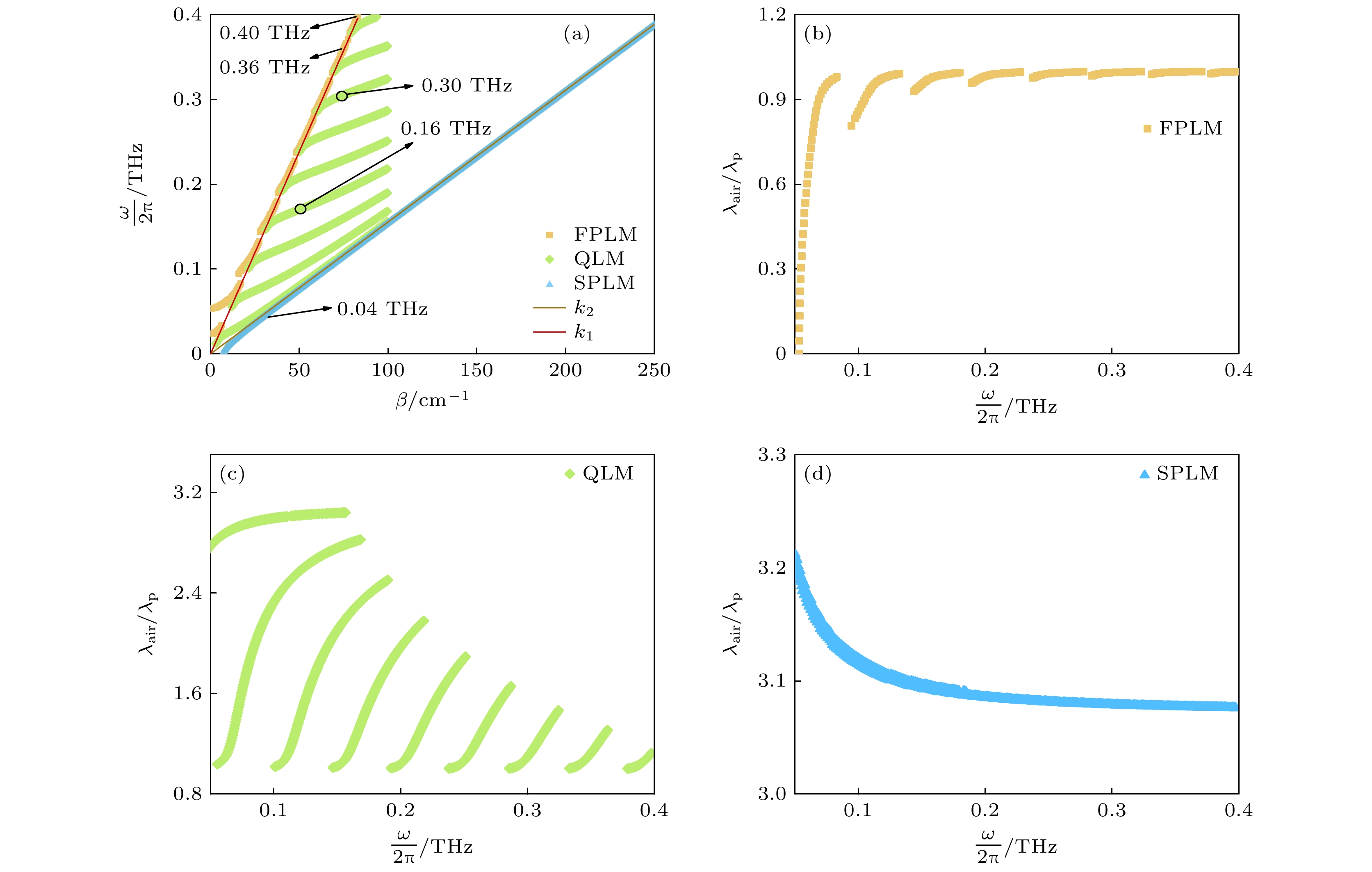
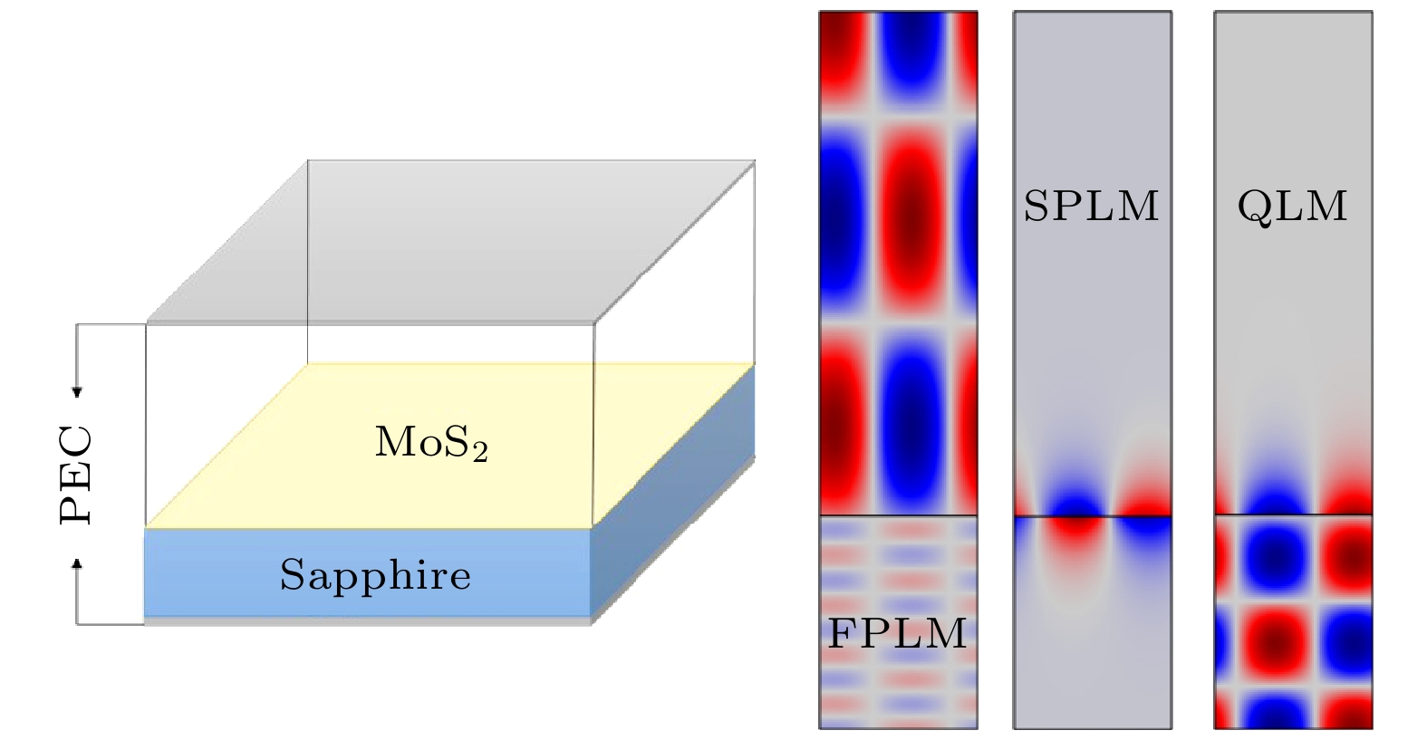
Compared with graphene, two-dimensional (2D) transition metal sulfides, represented by mono-/few-layer MoS2, have tunable non-zero bandgap, and thus their applications in optoelectronic devices are more advantageous. By using classical electromagnetic theory and finite element method (FEM), we investigate the cavity coupled plasmon polaritons (CCPPs) formed through the coupling between cavity modes in a resonator and plasmons in monolayer MoS2, particularly calculate and verify the properties of the high-order CCPPs. In previous work, it was demonstrated that the substrates, defects, and polycrystalline grains of the CVD grown monolayer MoS2 usually induce weak electron localization, which leads to the deviation from the Drude model based on the approximation of free electron gas. Therefore, here we use the Drude-Smith model with characteristic parameters obtained experimentally to describe the optical conductivity of monolayer MoS2 in our theoretical calculation and simulation. Then, we not only derive and solve the dispersion equations of the high-order CCPPs, but also verify the existence and analyze the properties of these high-order modes. Specifically, there are three types of CCPPs in the asymmetric cavity-monolayer MoS2 system, i.e. the FP-like-modes (FPLMs), the surface-plasmon-like modes (SPLMs), and the quasi-localized modes (QLMs). Among them, the FPLMs and QLMs can support high-order modes whereas the SPLMs only support the fundamental modes. According to our model, we calculate the wave localization properties for the 7th-order and 8th-order FPLM, the 3rd-order and 6th-order QLM, and the SPLM. These theoretical results are in good agreement with the simulation results. Moreover, the effects of weak electron localization are also shown by comparing the field distributions of the CCPPs based on the Drude model with those based on the Drude-Smith model. It is found that weak electron localization can reduce the coupling between the cavity modes and the plasmons in monolayer MoS2. These results can deepen our understanding of the excitation of plasmons in 2D materials as well as the modulation of their properties. Furthermore, the theoretical model can also be extended to other plasmonic systems related to low-dimensional and topological quantum materials.
-
Keywords:
- plasmons /
- monolayer MoS2 /
- cavity /
- terahertz
[1] Novoselov K S, Geim A K, Morozov S V, Jiang D, Zhang Y, Dubonos S V, Grigorieva I V, Firsov A A 2004 Science 306 666
 Google Scholar
[2] Geim A K, Novoselov K S 2007 Nat. Mater. 6 183
 Google Scholar
[3] Fan Y C, Shen N H, Zhang F L, Zhao Q, Wu H J, Fu Q H, Wei Z Y, Li H Q, Soukoulis C M 2019 Adv. Opt. Mater. 7 1800537
 Google Scholar
[4] Lu W, Ling J W, Xiu F X, Sun D 2018 Phys. Rev. B 98 104310
 Google Scholar
[5] Hou L, Yang Y K, Li A L, Wang Q J, Li Q N, Wu M, Ji P C, Zhang Y J, Xiao Y M, Xu W, Xiu F X, Ding L 2023 Phys. Rev. B 108 115416
 Google Scholar
[6] Mak K F, Lee C, Hone J, Shan J, Heinz T F 2010 Phys. Rev. Lett. 105 136805
 Google Scholar
[7] Wang Q H, Kalantar-Zadeh K, Kis A, Coleman J N, Strano M S 2012 Nat. Nanotechnol. 7 699
 Google Scholar
[8] Manzeli S, Ovchinnikov D, Pasquier D, Yazyev O V, Kis A 2017 Nat. Rev. Mater. 2 17033
 Google Scholar
[9] Liu X, Hou L, Ji P C, Wang Q J, Wu M, Xiao Y M, Xu W, Ding L 2023 Nanophotonics 12 4441
 Google Scholar
[10] Liu H, Neal A T, Zhu Z, Luo Z, Xu X F, Tomanek D, Ye P D 2014 ACS Nano 8 4033
 Google Scholar
[11] Qiao J, Kong X, Hu Z X, Yang F, Ji W 2014 Nat. Commun. 5 4475
 Google Scholar
[12] Zhang S J, Pei Y F, Hu S Q, Wu N, Chen D Q, Lian C, Meng S 2023 Chin. Phys. Lett. 40 077502
 Google Scholar
[13] Liu X Z, Galfsky T, Sun Z, Xia F N, Lin E C, Lee Y H, Kena-Cohen S, Menon V M 2015 Nat. Photonics 9 30
 Google Scholar
[14] Kleemann M E, Chikkaraddy R, Alexeev E M, Kos D, Carnegie C, Deacon W, Pury A C de, Grosse C, Nijs B de, Mertens J, Tartakovskii A I, Baumberg J J 2017 Nat. Commun. 8 1296
 Google Scholar
[15] Verre R, Baranov D G, Munkhbat B, Cuadra J, Kall M, Shegai T 2019 Nat. Nanotechnol. 14 679
 Google Scholar
[16] Liu W J, Lee B, Naylor C H, Ee H S, Park J, Johnson A T C, Agarwal R 2016 Nano Lett. 16 1262
 Google Scholar
[17] Hu G W, Krasnok A, Mazor Y, Qu C W, Alu A 2020 Nano Lett. 20 3217
 Google Scholar
[18] Sun B, Wang Z, Liu Z, Tan X, Liu X, Shi T, Zhou J, Liao G 2019 Adv. Funct. Mater. 29 1900541
 Google Scholar
[19] Leng Q, Su H, Liu J, Zhou L, Qin K, Wang Q, Fu J, Wu S, Zhang X 2021 Nanophotonics 10 1871
 Google Scholar
[20] Lan H Y, Hsieh Y H, Chiao Z Y, Jariwala D, Shih M H, Yen T J, Hess O, Lu Y J 2021 Nano Lett. 21 3083
 Google Scholar
[21] Petrić M M, Kremser M, Barbone M, Nolinder A, Lyamkina A, Stier A V, Kaniber M, Müller K, Finley J J 2022 Nano Lett. 22 561
 Google Scholar
[22] Zhu Y X, Yang J W, Abad-Arredondo J, Fernández-Domínguez A I, Garcia-Vidal F J, Natelson D 2024 Nano Lett. 24 525
 Google Scholar
[23] Wang C, Xu W, Mei H Y, Qin H, Zhao X N, Zhang C, Yuan H F, Zhang J, Xu Y, Li P, Li M 2019 Opt. Lett. 44 4139
 Google Scholar
[24] Liu J, Ding L, Zhao C X, Liang C N, Xiao Y M, Zhang J, Xu W 2019 IEEE Photonics J. 11 4800608
[25] Guo T Y, Hou L, Xu W, Xiao Y M, Ding L 2022 J. Opt. Soc. Am. B: Opt. Phys. 39 1711
 Google Scholar
[26] Ding L, Xu W, Zhao C, Wang S, Liu H 2015 Opt. Lett. 40 4524
 Google Scholar
[27] Maier S A 2007 Plasmonics: Fundamentals and Applications (New York: Springer) p21
-
图 2 (a) 单层MoS2光电导率随频率的变化; (b) 蓝宝石衬底的复折射率随频率的变化. 图(a)中使用普适电导率$\varSigma_0 = e^2/4 \hbar $对光电导率实部和虚部做归一化
Figure 2. (a) Frequency dependency of optical conductivity of monolayer MoS2; (b) frequency dependency of the complex refractive index of the sapphire substrate. In panel (a) both the real and imaginary parts of the optical conductivity are normalized by universal conductivity $\varSigma_0 = e^2/4 \hbar $.
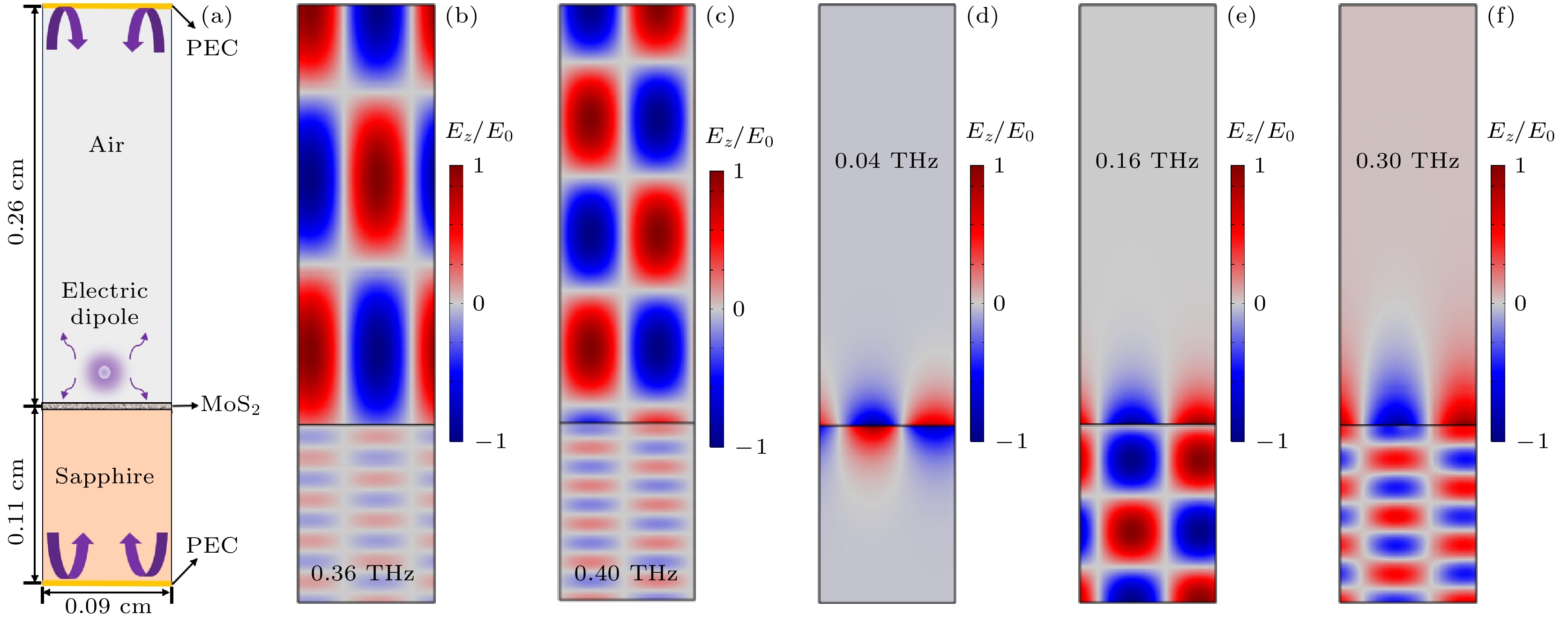
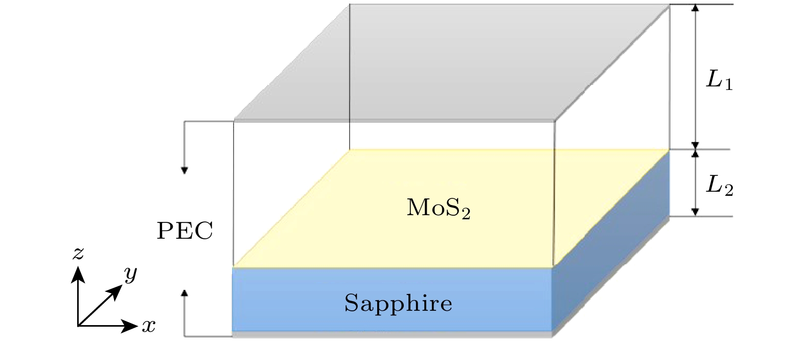
图 4 CCPP的FEM模拟 (a) 模拟模型示意图; (b) NF = 7和(c) NF = 8时FPLM, (d) 基模SPLM以及(e) NQ = 3和(f) NQ = 6时QLM的电磁场Ez空间分布. 注意此处电场分量Ez都已使用各自的最大值E0做了归一化
Figure 4. FEM simulation results of the CCPPs: (a) Diagram of the simulation model. Field distributions of Ez for the FPLMs of (b) NF = 7 and (c) NF = 8, (d) the fundamental mode of SPLM, and the QLMs of (e) NQ = 3 and (f) NQ = 6. Note that the fields Ez are normalized by the corresponding maximum values E0.
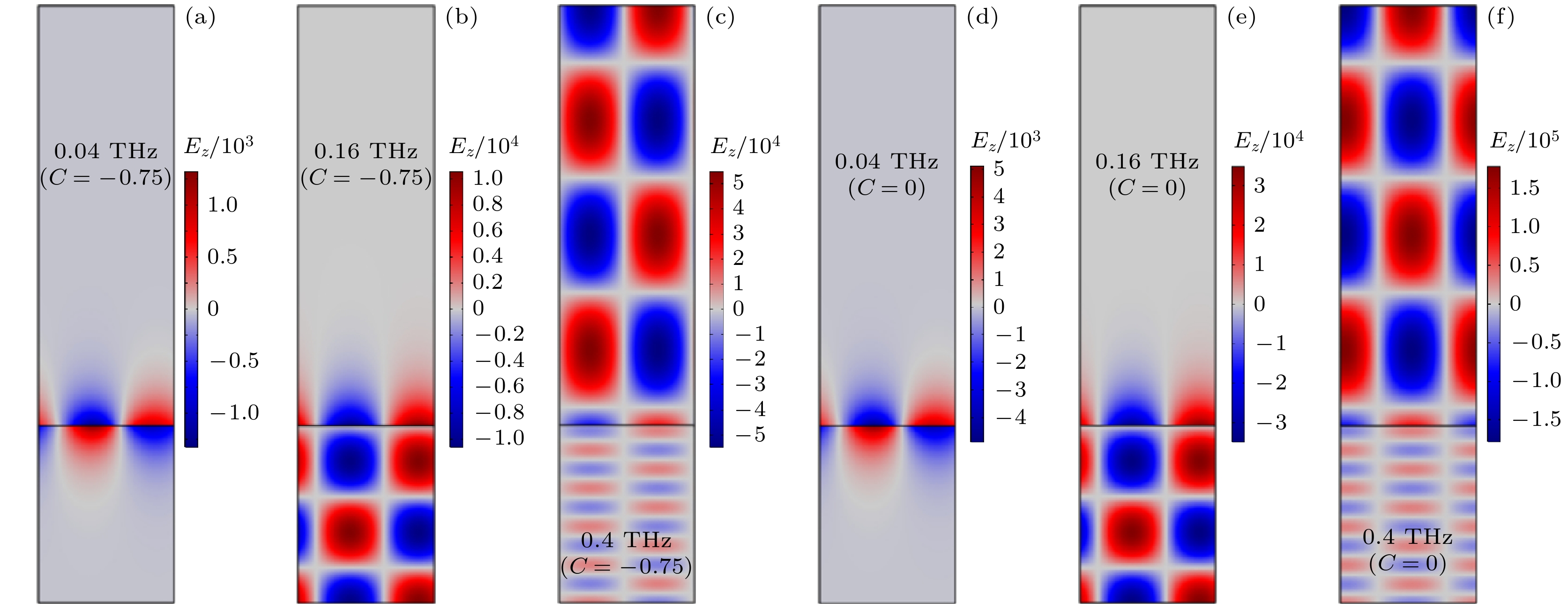
图 5 局域因子C不同时, CCPP的FEM模拟 (a)—(c) C = –0.75时的SPLM (a), QLM (b)及FPLM (c); (d)—(f) C = 0 时的SPLM (d), QLM (e)及FPLM (f). 注意此处电场分量Ez都未做归一化
Figure 5. FEM simulation results of the CCPPs with different C: (a)–(c) Field distributions of (a) SPLM, (b) QLM, and (c) FPLM for C = –0.75; (d)–(f) results of (d) SPLM, (e) QLM, and (f) FPLM for C = 0. Note that the fields Ez are not normalized.
-
[1] Novoselov K S, Geim A K, Morozov S V, Jiang D, Zhang Y, Dubonos S V, Grigorieva I V, Firsov A A 2004 Science 306 666
 Google Scholar
[2] Geim A K, Novoselov K S 2007 Nat. Mater. 6 183
 Google Scholar
[3] Fan Y C, Shen N H, Zhang F L, Zhao Q, Wu H J, Fu Q H, Wei Z Y, Li H Q, Soukoulis C M 2019 Adv. Opt. Mater. 7 1800537
 Google Scholar
[4] Lu W, Ling J W, Xiu F X, Sun D 2018 Phys. Rev. B 98 104310
 Google Scholar
[5] Hou L, Yang Y K, Li A L, Wang Q J, Li Q N, Wu M, Ji P C, Zhang Y J, Xiao Y M, Xu W, Xiu F X, Ding L 2023 Phys. Rev. B 108 115416
 Google Scholar
[6] Mak K F, Lee C, Hone J, Shan J, Heinz T F 2010 Phys. Rev. Lett. 105 136805
 Google Scholar
[7] Wang Q H, Kalantar-Zadeh K, Kis A, Coleman J N, Strano M S 2012 Nat. Nanotechnol. 7 699
 Google Scholar
[8] Manzeli S, Ovchinnikov D, Pasquier D, Yazyev O V, Kis A 2017 Nat. Rev. Mater. 2 17033
 Google Scholar
[9] Liu X, Hou L, Ji P C, Wang Q J, Wu M, Xiao Y M, Xu W, Ding L 2023 Nanophotonics 12 4441
 Google Scholar
[10] Liu H, Neal A T, Zhu Z, Luo Z, Xu X F, Tomanek D, Ye P D 2014 ACS Nano 8 4033
 Google Scholar
[11] Qiao J, Kong X, Hu Z X, Yang F, Ji W 2014 Nat. Commun. 5 4475
 Google Scholar
[12] Zhang S J, Pei Y F, Hu S Q, Wu N, Chen D Q, Lian C, Meng S 2023 Chin. Phys. Lett. 40 077502
 Google Scholar
[13] Liu X Z, Galfsky T, Sun Z, Xia F N, Lin E C, Lee Y H, Kena-Cohen S, Menon V M 2015 Nat. Photonics 9 30
 Google Scholar
[14] Kleemann M E, Chikkaraddy R, Alexeev E M, Kos D, Carnegie C, Deacon W, Pury A C de, Grosse C, Nijs B de, Mertens J, Tartakovskii A I, Baumberg J J 2017 Nat. Commun. 8 1296
 Google Scholar
[15] Verre R, Baranov D G, Munkhbat B, Cuadra J, Kall M, Shegai T 2019 Nat. Nanotechnol. 14 679
 Google Scholar
[16] Liu W J, Lee B, Naylor C H, Ee H S, Park J, Johnson A T C, Agarwal R 2016 Nano Lett. 16 1262
 Google Scholar
[17] Hu G W, Krasnok A, Mazor Y, Qu C W, Alu A 2020 Nano Lett. 20 3217
 Google Scholar
[18] Sun B, Wang Z, Liu Z, Tan X, Liu X, Shi T, Zhou J, Liao G 2019 Adv. Funct. Mater. 29 1900541
 Google Scholar
[19] Leng Q, Su H, Liu J, Zhou L, Qin K, Wang Q, Fu J, Wu S, Zhang X 2021 Nanophotonics 10 1871
 Google Scholar
[20] Lan H Y, Hsieh Y H, Chiao Z Y, Jariwala D, Shih M H, Yen T J, Hess O, Lu Y J 2021 Nano Lett. 21 3083
 Google Scholar
[21] Petrić M M, Kremser M, Barbone M, Nolinder A, Lyamkina A, Stier A V, Kaniber M, Müller K, Finley J J 2022 Nano Lett. 22 561
 Google Scholar
[22] Zhu Y X, Yang J W, Abad-Arredondo J, Fernández-Domínguez A I, Garcia-Vidal F J, Natelson D 2024 Nano Lett. 24 525
 Google Scholar
[23] Wang C, Xu W, Mei H Y, Qin H, Zhao X N, Zhang C, Yuan H F, Zhang J, Xu Y, Li P, Li M 2019 Opt. Lett. 44 4139
 Google Scholar
[24] Liu J, Ding L, Zhao C X, Liang C N, Xiao Y M, Zhang J, Xu W 2019 IEEE Photonics J. 11 4800608
[25] Guo T Y, Hou L, Xu W, Xiao Y M, Ding L 2022 J. Opt. Soc. Am. B: Opt. Phys. 39 1711
 Google Scholar
[26] Ding L, Xu W, Zhao C, Wang S, Liu H 2015 Opt. Lett. 40 4524
 Google Scholar
[27] Maier S A 2007 Plasmonics: Fundamentals and Applications (New York: Springer) p21
Catalog
Metrics
- Abstract views: 3306
- PDF Downloads: 89
- Cited By: 0


 DownLoad:

