


Vol. 70, No. 19 (2021)
2021-10-05
REVIEW

EDITOR'S SUGGESTION
2021, 70 (19): 198102.
doi: 10.7498/aps.70.20210531
Abstract +
In recent years, mobile consumer electronics and electric vehicles have been developing rapidly, and they have been hunting for lithium batteries with high energy density, high safety and stability, to alleviate the range anxiety and improve their stability over long term operations. These make all-solid-state lithium batteries very attractive and they have been under intense investigations. However, the development of high-performance all-solid-state lithium batteries requires an in-depth understanding of their charge and discharge mechanism, their degradation process, along with the evolution of the microstructures, phase compositions, chemical states and their distributions, etc., inside the battery and at the interface. This paper summarizes the basic principles, functions, and the representative advances in investigation of the dynamics and failure mechanism of electrode materials and interfaces in solid-state lithium batteries under working conditions, with typical in-situ characterization techniques, including in-situ microscopy (in-situ scanning electron microscopy (SEM), in-situ transmission electron microscopy (TEM)), in-situ X-ray techniques (in-situ X-ray diffraction (XRD)), in-situ X-ray photoelectron spectroscopy (XPS), in-situ near-edge structure X-ray absorption spectroscopy (XANES), in-situ X-ray tomography), in-situ neutron techniques (in-situ neutron diffraction (ND), in-situ neutron depth profiling (NDP)) and in-situ spectroscopies (in-situ Raman spectroscopy, in-situ nuclear magnetic resonance (NMR) and in-situ nuclear magnetic resonance imaging (MRI)), etc. We also discussed the application of future advanced in-situ characterization techniques in the investigation of all-solid-state lithium batteries.


EDITOR'S SUGGESTION
2021, 70 (19): 198501.
doi: 10.7498/aps.70.20210652
Abstract +
Superconducting nanowire single photon detector (SNSPD) plays a significant role in plenty of fields such as quantum information, deep space laser communication and lidar, while the mechanism of the photon response process still lacks a recognized theory. It is prerequisite and essential for fabricating high-performance SNSPD to understand in depth and clarify the photon response mechanism of the SNSPD. As mature theories on the SNSPD response progress, hot-spot model and vortex-based model both have their disadvantages: in the former there exists the cut-off wavelength and in the later there is the size effect, so they both need further improving. The Cut-off wavelength means that the detection efficiency of the SNSPD drops to zero with the increase of light wavelength, which is indicated by the hot-spot model but not yet observed in experiment. The size effect implies that the vortex does not exist in the weak link with the width less than 4.41ξ, where ξ is the GL coherence length. Phase slip is responsible for the intrinsic dissipation of superconductors, which promises to expound the SNSPD photon response progress and to establish a complete theory. This paper reviews and discusses the fundamental conception, the development history and the research progress of the hot-spot models, i.e. the vortex-based model and the superconductor phase slips, providing a reference for studying the SNSPD photon response mechanism.
GENERAL
2021, 70 (19): 190201.
doi: 10.7498/aps.70.20210083
Abstract +
Yb-doped fiber laser is a very appealing technology to implement space communication, laser radar and nuclear facilities due to its reduced weight, size, high efficiency, high peak power combined with good beam quality. However, Yb-doped fiber materials will suffer a harsh ionizing radiation (such as neutron, proton and electron) under the condition of irradiation. The radiation-induced darkening effect can lead the fiber loss to increase obviously, the laser slope efficiency to decrease drastically, and even no laser output to be observed in severe cases. Therefore, it is necessary to conduct in-depth research on the performance changes of Yb-doped fiber materials subjected to the irradiation. In this paper, a series of Yb-doped optical fibers and optical fibers is prepared by the improved chemical vapor deposition method combined with rare-earth chelate-doped. And the optical properties of the optical fiber before and after being irradiated and annealed are tested. We mainly investigate the absorption spectrum of Yb-doped fiber material. The results show that the concentration of Al-related defects in the Yb-doped fiber material increases after neutron irradiation, and the absorption loss in the visible region increases. And the color center defects produced by the irradiation will significantly reduce the Yb ion fluorescence lifetime. The doping of Ce ions can reduce the Al-oxygen hole center (Al-OHC) color center defects, and can suppresse the radiation-induced darkening effect of Yb-doped fiber to a certain extent. Thermal annealing can reduce the absorption of fiber material by reducing the concentration of neutron radiation-induced color center defects, and thus eliminating the darkening effect to a certain extent. Finally, with our previous research, we find that neutron irradiation and ray irradiation have similar effects on the optical properties of Yb-doped fiber materials. The main reason is that the electron ionization effects occur due to both ray irradiation and neutron irradiation to generate free electron and hole pairs, which then combine with the original defects in the material to turn into color center defects. However, the color center defects caused by neutron irradiation are more stable and require thermal annealing to be eliminated. And the results obtained in this study provide theoretical basis and solution for developing the Yb-doped fibers with high laser performance and high radiation resistance.

2021, 70 (19): 190202.
doi: 10.7498/aps.70.20202147
Abstract +
The variational iteration method, based on the variational principle, is a numerical format with high numerical accuracy and convenience, has been widely applied in the numerical solution of various strong-nonlinear solitary wave equations. In this paper, the modified variational iteration method is used to improve the original numerical method, that is, the parameter h is introduced before the variational item. By defining the discrete two norm of the error function and drawing the h-curve in the domain of definition, the h that minimizes the error is determined and then returned to the original iteration process for solution. In this paper, We choose the uniform grid points to caculate the error. At the same time, the introduction of parameters also expands the convergence domain of the original numerical solution and achieves the numerical optimization under the condition of a certain number of iterations, which shows better than the general method. In the numerical experiment, the above results are applied to the fourth-order Cahn-Hilliard equation and the Benjamin-Bona-Mahony-Burgers equation. The Cahn-Hilliard equation was first found to describe the phenomeno in interface dynamics. It has vital application in physical. For the fourth-order Cahn-Hilliard equation, the error order of the ordinary variational iteration method is about $10^{-1}$ , and the absolute error is reduced to $10^{-4}$ after the modification. Moreover, the modified method expands the convergence domain of the original numerical solution. And the Benjamin-Bona-Mahony-Burgers equation can be degenerated to the Benjamin-Bona-Mahony and the Burgers equation under the appropriate parameter selection. For the Benjamin-Bona-Mahony-Burgers equation, if using the normal method, we can find that the numerical solution will not converge. But the accuracy of the numerical solution is decreased to $10^{-3}$ by using the variational iteration method with auxiliary parameters, which is superior to the original variational iteration method in the approximation effect of the true solution. This numerical method also provides a scheme and reference for the numerical solution of other strong-nonlinear solitary wave differential equations. This scheme provieds a continuous solution in the time and space domain, which differs from the finite difference method, finite volume scheme and so on. That means we can use this method independently without using any other scheme to match our approarch, this is also the advantage of the modified variational iteration method.


EDITOR'S SUGGESTION
2021, 70 (19): 190301.
doi: 10.7498/aps.70.20210837
Abstract +
Quantum state that carries classical information, 0 or 1, can be safely and reliably transmitted using quantum secure direct communication. How to transmit an arbitrary quantum state is a wider issue and has important applications. One way is to use quantum teleportation, namely, first distribute a large number of Einstein-Podolsky-Rosen pairs, and then perform entanglement purification to obtain a near-perfect pair, and make quantum teleportation using the pair. In this article, we propose a method that directly port the quantum state with security and reliability using quantum secure direct communication. After sufficient number of copies of the same state have been directly ported, single-particle purification is performed to obtain a near perfect single particle state. This is important because it offers a new method for sending an arbitrary single particle state securely and reliably without using quantum teleportation. It is also an important extension of quantum secure direct communication to send an arbitrary quantum state. Quantum direct portation will have great potential in quantum internet.
2021, 70 (19): 190501.
doi: 10.7498/aps.70.20210517
Abstract +
2021, 70 (19): 190502.
doi: 10.7498/aps.70.20202063
Abstract +
The diffusion dynamics of a particle in the biased disorder medium is investigated in this paper. Based on the mean first passage time (MFPT) theory, the analytical approximate expression of effective diffusion coefficient of a particle in the biased disorder potential is obtained. The results show that the effective diffusion of a particle in the biased disorder potential is significantly enhanced. We explain the enhancement mechanism by using the wave packet broadening of probability density distribution function. In addition, we propose the concepts of effective kinetic temperature and effective friction, and further find that the effective diffusion behavior of a particle strongly depends on the biased force.
THE PHYSICS OF ELEMENTARY PARTICLES AND FIELDS

2021, 70 (19): 191401.
doi: 10.7498/aps.70.20210804
Abstract +
Muon scattering imaging technology can be used to detect nuclear material and is of considerable significance in nuclear safety. However, it is difficult to distinguish special nuclear materials from high-Z objects effectively by using the existing muon scattering imaging technologies. Muon-induced neutrons emitted from special nuclear materials can help to identify the existence of special nuclear materials. However, this method has long imaging time and low imaging quality. Multimodal imaging of muon uses both the information about scattering muons penetrating the material and the information about muons stopped by material and generating secondary induced neutrons, which can overcome the shortcomings of single imaging method effectively. The detection model is set up based on Geant4. The simulation programs of muon imaging in coincidence with muon induced neutrons, scattering imaging of muon, and multimodal imaging of muon are developed by using Cosmic-ray Shower Library as particle source, and the imaging algorithms are implemented respectively on the basis of the simulated data. Two imaging models are designed for muon scattering imaging. The first one is a single 235U cube, and the second one is composed of four cubes, namely 235U cube, 239Pu cube, lead cube and aluminum cube. This simulation has completed muon scattering imaging of single cube and four cubes. In the part of muon imaging in coincidence with muon induced neutrons, the neutronic gain of the HEU (90% 235U) plate, LEU (20% 235U) plate, and DU (0.2% 235U) plate, as well as the relationship between the neutronic gain of these three uranium plates and the energy and charged properties of the muon are obtained by simulation, and then two imaging models are set up. The first one is composed of four cubes, namely 235U cube, 239Pu cube, lead cube, and aluminum cube, and the other is comprised of multilayer nuclear components. The 2D and 3D reconstruction results of multi-objects and multilayer nuclear components are obtained through muon imaging in coincidence with muon induced neutrons. Then the multimodal imaging of muon for three cubes is realized in the presence or absence of iron shielding shell. The imaging capabilities are compared with the muon scattering imaging capacities and muon imaging capacities in coincidence with muon induced neutrons. Simulation studies indicate that multimodal imaging of muon based on scattering and secondary induced neutrons can effectively combine the advantages of every single imaging method. The multimodal imaging of muon can take advantage of available information more efficiently, which is helpful in improving the imaging quality. Multimodal imaging of muon not only has the advantages of short imaging time and high imaging quality, but also can distinguish special nuclear material from other high-Z materials clearly, which is vital for detecting special nuclear materials.
NUCLEAR PHYSICS
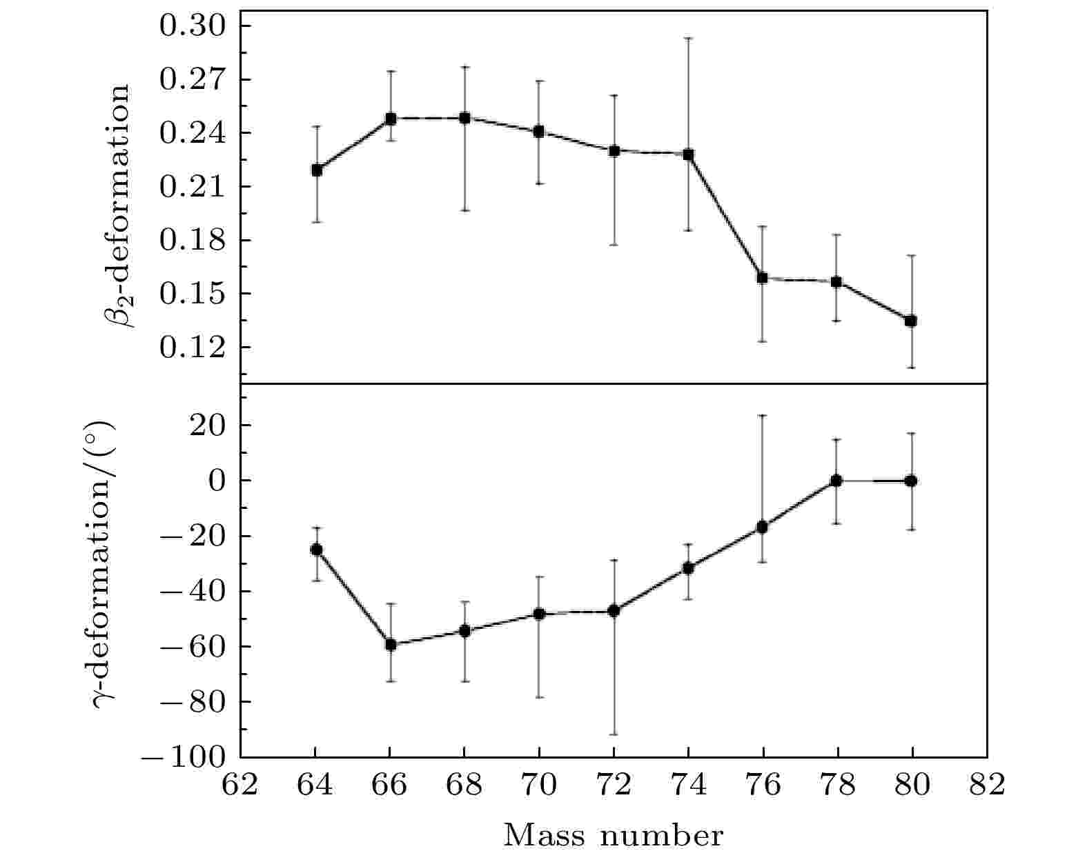
2021, 70 (19): 192101.
doi: 10.7498/aps.70.20210187
Abstract +
Evidence for nonaxial γ deformations has been widely found in collective rotational states. The γ deformation has led to very interesting characteristics of nuclear motions, such as wobbling, chiral band, and signature inversion in rotational states. There is an interesting question; why the nonaxial γ deformation is not favored in the ground states of even-even (e-e) nuclei. The quest for stable triaxial shapes in the ground states of e-e nuclei, with a maximum triaxial deformation of $ \left| \gamma \right| $ ≈ 30°, is still a major theme in nuclear structure. In the present work, we use the cranked Woods-Saxon (WS) shell model to investigate possible triaxial shapes in ground and collective rotational states. Total-Routhian-surface calculations by means of the pairing-deformation-frequency self-consistent cranked shell model are carried out for even-even germanium and selenium isotopes, in order to search for possible triaxial deformations of nuclear states. Calculations are performed in the lattice of quadrupole (β2, γ) deformations with the hexadecapole β4 variation. In fact, at each grid point of the quadrupole deformation (β2, γ) lattice, the calculated energy is minimized with respect to the hexadecapole deformation β4. The shape phase transition from triaxial shape in 64Ge, oblate shape in 66Ge, again through triaxiality, to prolate deformations is found in germanium isotopes. In general, the Ge and Se isotopes have γ-soft shapes, resulting in significant dynamical triaxial effect. There is no evidence in the calculations pointing toward rigid triaxiality in ground states. The triaxiality of $ \gamma = - 30^\circ $ for the ground and collective rotational states, that is the limit of triaxial shape, is found in 64, 74Ge. One should also note that the depth of the triaxial minimum increases with rotational frequency increasing in these two nuclei. The present work focuses on the possible triaxial deformation of N = Z nucleus 64Ge. Single-particle level diagrams can give a further understanding of the origin of the triaxiality. Based on the information about single-particle levels obtained with the phenomenological Woods-Saxon (WS) potential, the mechanism of triaxial deformation in N = Z nucleus 64Ge is discussed, and caused surely by a deformed γ≈30° shell gap at Z(N) = 32. At N = 34, however, an oblate shell gap appears, which results in an oblate shape in 66Ge (N = 34). With neutron number increasing, the effect from the N = 34 oblate gap decreases, and hence the deformations of heavier Ge isotopes change toward the triaxiality (or prolate).


ATOMIC AND MOLECULAR PHYSICS
EDITOR'S SUGGESTION

2021, 70 (19): 193201.
doi: 10.7498/aps.70.20210757
Abstract +


2021, 70 (19): 193601.
doi: 10.7498/aps.70.20210645
Abstract +
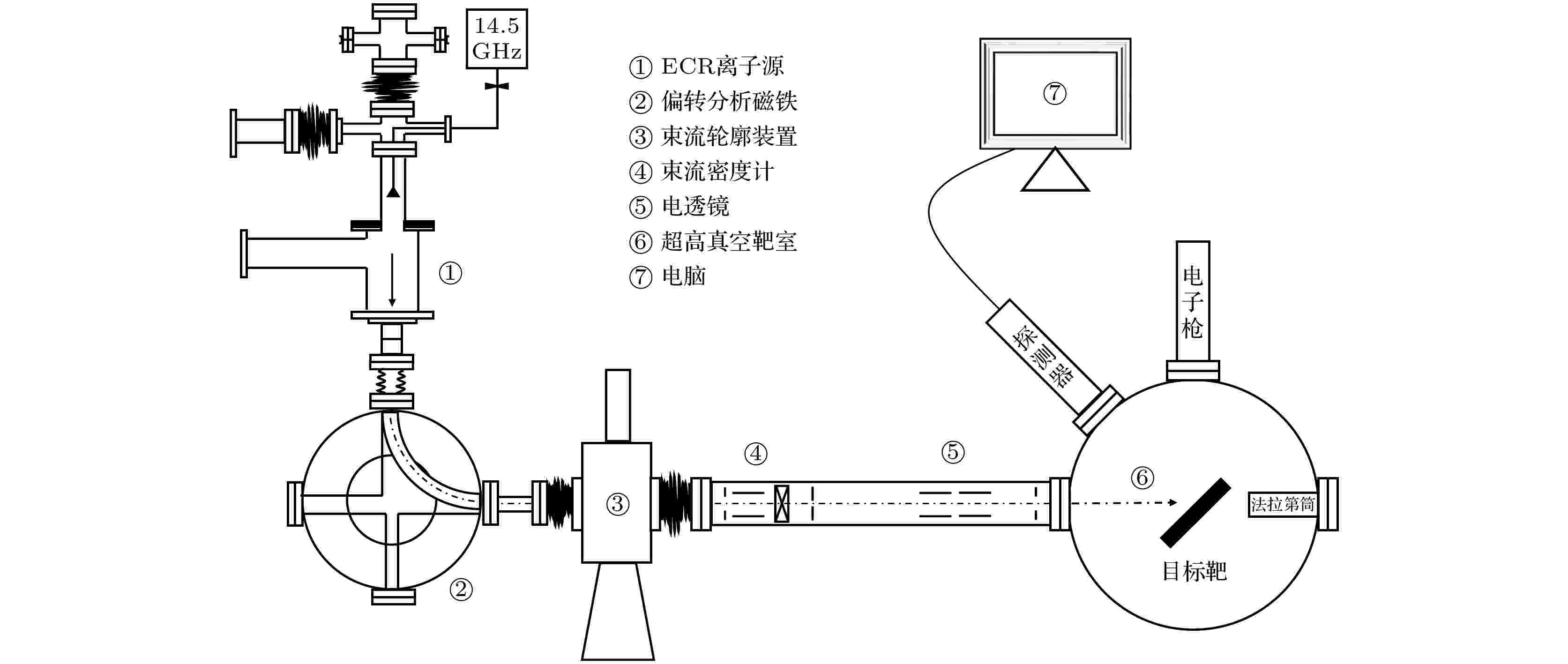
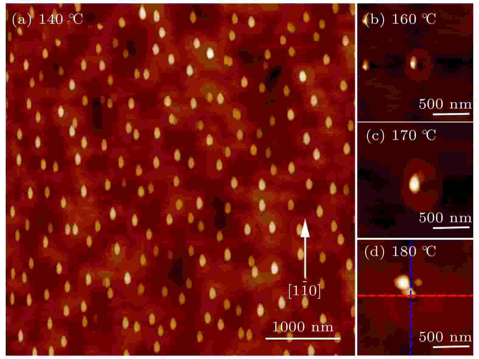
In recent years, low-dimensional nanostructures such as quantum dots (QD) and quantum rings (QR) have been widely used in many fields such as optoelectronics, microelectronics and quantum communication due to their unique electrical, optical and magnetic properties. Owing to the similarity between nanostructures and atomic systems, the flexible modulation of several quantum properties of nanomaterials and the preparation of new optoelectronic devices around the characteristics of these structural systems have become a hot topic of research. Changing the growth process to control and tune the atomic diffusion mechanism in droplets is a key way of preparing complex nanostructures, which is important for the study of semiconductor nanostructure by droplet epitaxy. In the present experiment, the same amount (5 monolayer (5 ML)) of indium is deposited on GaAs (001) at different substrate temperatures (140, 160, 170 and 180 ℃) and different arsenic pressures (1.6, 3.3 and 4.6 ML/s), and the surface morphology evolutions are observed. As the substrate temperature increases, the radius of the disk gradually expands and a pit appears in the center of the diffusion disk. As the arsenic pressure increases, the density of the formed droplets increases, and the width of the diffusion disk formed in the center of the droplets gradually decreases. Our work involving nucleation theory is done at T < 200 ℃ to deactivate many thermal processes. This is a result of the diffusion coefficient being more complexly related to temperature. Based on the classical nucleation diffusion theory, the results of experimental data fitting include that the diffusion activation energies of In atoms on the surface of GaAs (001) are (0.62 ± 0.01) eV in $ [1\bar 10] $ and (1.37 ± 0.01) eV in [110] respectively, and that the diffusion coefficient D0 is 1.2 × 10⁻² cm2/s:those results confirm the theory after having been compared with the results obtained by other research groups. The diffusion activation energy of indium atoms and the diffusion mechanism of indium droplets on GaAs (001) obtained from the experiment can provide experimental guidance for modulating the structural property of InAs nanostructures.


EDITOR'S SUGGESTION
2021, 70 (19): 193701.
doi: 10.7498/aps.70.20210778
Abstract +
Using a state-of-the-art numerical method density-matrix renormalization-group, we study the ground states of one-dimensional spinless Bose-Hubbard model inside a red-detuned cavity. By calculating the superfluid order, density distribution, second and third-order correlation functions, we find that there exist two novel supersolid phases with diagonal, off-diagonal orders beyond mean-field theory. One has package type density modulation along the lattice axis, another exhibits uniform density distribution. Moreover, by calculating the superradiant order parameter and the number of photon inside the cavity, we find that the novel supersolid phases are highly related to cavity-field fluctuation. Our work gives the physics beyond the mean-field theory of the Bose-Hubbard model inside an optical cavity, and provides the complete approach to fully explore the collective state of light and matter inside an optical cavity.
ELECTROMAGNETISM, OPTICS, ACOUSTICS, HEAT TRANSFER, CLASSICAL MECHANICS, AND FLUID DYNAMICS

2021, 70 (19): 194101.
doi: 10.7498/aps.70.20210746
Abstract +
Aiming at obtaining low scattering antenna array, in this paper a novel method of integrating electromagnetic metasurface with conventional antenna is proposed. The theoretical analysis and practical implementation of this method are presented. Using this method, a novel antenna array is obtained by connecting partial unit cells of metasurface with transmission line and adopting coaxial excitations. In the radiation mode, the metasurface is excited and radiates effectively. Besides, the array has almost the same performance as the conventional array. In the scattering mode, this array demonstrates low in-band RCS due to the scattering cancellation of middle metasurface and other surrounding structures. Using this method, a 2 × 1 array, as an example, is designed and numerically analyzed. The results show that the array has the well-behaved radiation performance and low RCS property. The working principle of the proposed array is illustrated by investigating the current and resultant field. Further analysis also reveals the effecting law of metasurface unit cells in antenna's radiation and scattering performance. Therefore, flexible designs can be obtained to fit different requirements. Finally, experiments are conducted. And the good agreement between computations and measurements further verifies the validity of the proposed design. Moreover, the proposed method also features easy implementation and high integrity and can be extended to the designing of large scale array antennas.

2021, 70 (19): 194201.
doi: 10.7498/aps.70.20210070
Abstract +
The electromagnetically induced transparency (EIT), which is a result of destructive interference between different excitation paths in a three-energy-level atomic medium, makes opaque probe light transparent over a range of frequencies. As this EIT effect is usually accompanied with strong dispersion, it has potential applications such as slow light propagation, optical buffering, nonlinear optics, optical sensing, etc. However, for conventional quantum EIT effect which requires stable gas lasers and low temperature environment, the implementation of EIT in chip-scale applications is severely hampered by the scathing experimental requirements. Recently, the EIT-like effect in metamaterials, which are constructed by designing the artificial subwavelength functional elements and arranging the spatial sequences, attracts tremendous attention because of its advantages, such as room temperature manipulability, large bandwidth, and small sizes. In addition, the high-quality factor(Q) value obtained by EIT-like effect has great significance in designing the metamaterial-based devices. In this paper, we design an EIT-like metamaterial with such a structure. The unit cell of the proposed metamaterial is constructed by two asymmetric silicon blocks embedded on a silicon dioxide substrate. Meanwhile, we analyze its optical properties and EIT-like effects by using three-dimension (3D) FDTD method. Based on the coupled Lorentz model, the EIT-like effect of the designed metamaterial is investigated. Then, by employing the electric field distribution on the surface of the metamaterial, and combining with the three-level atomic system, the mechanism of the EIT-like effect is analyzed in detail. We find that the EIT-like effect in the proposed metamaterial has high Q value (Q ≈ 8616) and the high transmission (T = 96%). By changing the length of the silicon block to destroy the asymmetry of the metamaterial structure, an active tuning EIT-like effect is realized. Furthermore, the metamaterial structure has the advantages of low loss, easy preparation, and active-controllability. This study represents an innovative approach to designing the EIT-like metamaterial, which is expected to be useful for designing active tunable slow-light devices and highly sensitive optical sensors.
2021, 70 (19): 194301.
doi: 10.7498/aps.70.20210045
Abstract +
2021, 70 (19): 194302.
doi: 10.7498/aps.70.20202232
Abstract +
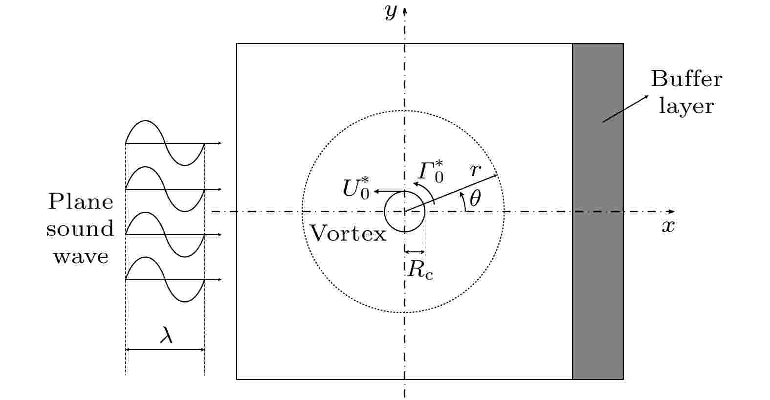
The scattering of acoustic waves by a vortex is a fundamental problem of the acoustic waves propagation in complex flow field, which plays an important role in academic research and engineering application for sound source localization, acoustic target recognition and detection, the far field noise prediction, such as aircraft wake vortex identification, detection and ranging, acoustic target forecasting in turbulent shear flow, acoustic measurement and sound source localization in wind tunnel test, etc. The nonlinear scattering phenomenon occurs when acoustic wave passes through the vortex, which is mainly related to the length-scale ratio between the wavelength of acoustic wave and the core radius of the vortex. In this paper, a plane acoustic wave passing through a stationary isentropic vortex is numerically simulated by solving a two-dimensional compressible, unsteady Euler equation. A sixth-order linear compact finite difference scheme is employed for spatial discretization. Time integration is performed by a four-stage fourth-order Runge-Kutta method. The eighth-order spatial compact filter scheme is adopted to suppress high frequency errors. At the far field boundaries, buffer layer is applied to handle the outgoing acoustic wave. Under the matching condition, the accuracy of the numerical results is verified by comparing with the previous direct numerical simulation results. The acoustic scattering cross-section method is introduced to analyze the effects of different length-scale ratio on the acoustic pulsation pressure, acoustic scattering effective sound pressure and acoustic scattering energy. Scattering occurs when sound waves pass through the vortex, the acoustic field in front of the vortex is basically unaffected, and the acoustic wave front remains intact. A “vacuum” region is formed slightly below the acoustic field directly behind the vortex, and two primary interference bands and several secondary interference bands are formed on the upper and lower sides of the vortex. As the length-scale ratio increases, the sound scattering decreases and the influence of the vortex flow field on the acoustic field gradually weakens. The influence region of effective sound pressure of acoustic scattering is mainly concentrated behind the vortex. With the increase of the length scale ratio, the influence gradually increases and extends to the upstream, and then the influence region gradually decreases to the vicinity of the vortex. When the length scale ratio is greater than or equal to 6, the location of the maximum effective sound pressure of sound scattering jumps from the upper right to the lower right of the vortex. The influence of acoustic wave wavelength change on the acoustic scattering energy can be divided into three parts. With the increase of the length scale ratio, the maximum sound scattering energy presents four different stages.
PHYSICS OF GASES, PLASMAS, AND ELECTRIC DISCHARGES

2021, 70 (19): 195201.
doi: 10.7498/aps.70.20210765
Abstract +
X-ray fluorescence computed tomography (XFCT) is a molecular imaging technique with great potential applications in biomedical imaging, in which used is the primary X-ray to excite element probes with high atomic number inside samples or tissues for functional imaging. However, owing to the limitation of molecular sensitivity and spatial resolution, the XFCT has not been widely used in the molecular imaging. A large number of Compton scattering photons are produced as the broadband primary X-ray passes through the samples or tissues, forming a strong noise background in the collected XRF signal, which is a major cause of limited molecular sensitivity. Therefore, eliminating the Compton scattering noise is very important for improving molecular sensitivity. In this paper, we summarize the main physical processes involved in the imaging process of XFCT, including the angle distribution and polarization state of the fluorescence and Compton scattering photons, fluorescence yield and deexcitation time of K-shell vacancy. The above physical processes are the main limitations of the imaging quality of XFCT. Through the derivation and analysis of physical processes, we explore the possibility of using these physical effects to reduce the Compton scattering noise and draw some conclusions below. 1) The deexcitation time of K-shell vacancy of the element with high atomic number is very short, consequently the scattered light and fluorescence cannot be distinguished between each other under the time resolution condition of the existing detector. 2) The angular distribution of the K-shell fluorescence emission is isotropic, and the differential cross section of Compton scattering reaches a minimum value near the polarization direction of the incident light of which the minimum decreases as the linear polarization degree of the incident light increases. Therefore, the polarized light source is beneficial to reducing the Compton scattering noise. 3) The linear degree of polarization of K-shell fluorescence is zero, while the Compton scattering photons possess a certain linear degree of polarization in some scattering directions, so the difference between polarization states may be helpful in reducing the Compton scattering noise.
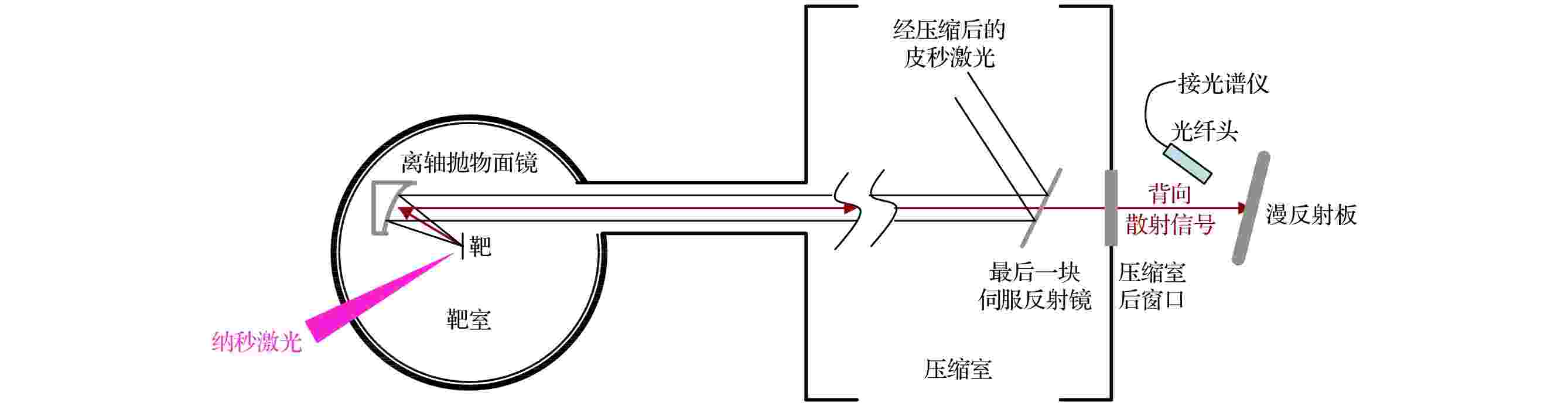
2021, 70 (19): 195202.
doi: 10.7498/aps.70.20210568
Abstract +
Laser plasma interaction (LPI) is an important content in laser plasma related research, and it is one of the key issues related to the success or failure of inertial confinement fusion ignition, and has received extensive attention. In order to suppress the relevant LPI process as much as possible, the major laboratories around the world have developed a variety of beam smoothing methods through decades of research. However, the current understanding and suppression of LPI are still far from enough, and further in-depth studies are still needed. Generally, the research of LPI is based on nanosecond laser driving, and focuses mainly on the effects of the related LPI process caused by nanosecond lasers. However, the LPI processes, such as stimulated Brillouin scattering (SBS), stimulated Raman scattering (SRS), etc., occur and develop on a time scale of picoseconds.The comprehensive effect can be studied only on a longer scale of nanosecond. For highly nonlinear LPI processes, the comprehensive effect may be difficult to reflect the real physical laws. The emergence of the picosecond laser has made it possible to study the LPI process in more detail and on a more appropriate time scale. The present research tries to gain an understanding of LPI from a more refined perspective. The experimental research of picosecond laser driving LPI is carried out on the Shenguang-Ⅱ upgrade and picosecond laser facilities. First, a nanosecond laser is used to irradiate a target to generate a large-scale plasma, and a few nanoseconds later, the picosecond laser is injected as an interaction beam to drive the LPI scattering such as SBS and SRS. The spectral signal of backscatter light is measured experimentally by using the method of diffuse reflector. From the research results it is found that the backward signals of the band near the laser wavelength contain, in addition to the true backward SBS component, a large number of interference signals introduced by picosecond laser and nanosecond laser. The interference signal introduced by nanosecond laser can be eliminated by using specific measures, but the interference signal introduced by picosecond laser cannot be eliminated experimentally, which will affect the estimation of the true share of the backward SBS. The comprehensive results show that under different experimental conditions, the backward scatter energy of SBS may be less than half that of the total recorded signals. This result is helpful in further understanding and re-recognizing previous relevant experimental data.
CONDENSED MATTER: STRUCTURAL, MECHANICAL, AND THERMAL PROPERTIES
2021, 70 (19): 196101.
doi: 10.7498/aps.70.20210621
Abstract +
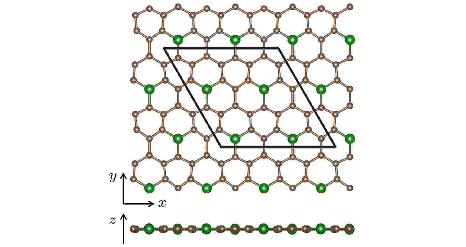
Siligraphene, as a composite of graphene and silicene, has attracted widespread attraction since it has many excellent properties that neither of graphene and silicene possesses. The properties of siligraphene are closely related to the distribution of Si atoms and its structure, but most of the current researches of siligraphene focus on the regular distribution of Si atoms and the planar structure with high symmetry. Therefore, we study in this work all possible Si atoms’ distributions with planar and nonplanar structures for siligraphene g-SiC7 based on density functional theory. At first, 365 kinds of inequivalent Si atoms’ distributions in g-SiC7 are selected out from the 35960 kinds of Si atoms’ distributions, and then for each inequivalent Si atoms’ distribution, a comparison of the stability between the planer and nonplanar structures is made. In terms of the Si distribution, the Si atoms tend to gather together to lower the energy. The more dispersed Si atoms’ distribution usually has appreciably higher energy. In terms of the planarity of the structures, it is found that there are many non-planar structures with significantly lower energy than the planar ones. For all possible Si atoms’ distributions, there are only 8 planar structures which are stable against out-of-plane perturbations. We further study the dynamic, thermodynamic and mechanical stability of the structures with the lowest energies and find that they are stable. The energy band calculation shows that two Dirac valleys still persist in the first Brillouin zone despite their appreciable structure deformation, and a considerable band gap is opened at the Dirac point. We calculate the Berry curvatures and find that the Berry curvatures at the inequivalent valleys are opposite, indicating that the system has valley degree of freedom. Our research shows that siligraphene is more likely to have a buckled structure and a more concentrated silicon atoms’ distribution, and the most stable structures have good electronic properties.

2021, 70 (19): 196401.
doi: 10.7498/aps.70.20210240
Abstract +
The equation of state (EOS) for CH material used as an ablator layer at high pressure is important in the study of implosion dynamics and target design for inertial confinement fusion (ICF). At present, most of EOS data are on the Hugoniot line under shock compression. The EOS data below Hugoniot line need further studying for low-entropy pre- compression. In the present article, the EOS of polystyrene is established under quasi-isentropic compression driven by HEAVEN-I KrF laser facility with a long rising edge (~20 ns). The shock dynamic behaviors of three kinds of CH targets are simulated, which are 100 μm CH planar target, Al-coated CH planar target (10 μm Al, 50 or 150 μm CH), and flyer-impact target composed of flyer (Al-coated CH), 100 μm vacuum layer, and 100 μm CH layer. The planar targets and flyer-impact targets with different thickness are irradiated by six-focused laser beams with total energy of 50–100J, and the free surface velocity and wave average transit velocity are measured by side-on shadowgraph technique. The simulation results indicate that the initial loading process is quasi-isentropic compression process, and then evolves into a weak shock compression process for the CH planar target in the rising edge stage. Comparing with the CH planar target, the reflected rarefaction waves from the Al-CH interface of Al-coated CH target can suppress the enhancement of compression wave, and delay the formation of shock wave when laser directly irradiates the Al layer. The shock pressure of the CH target layer (the third layer) is significantly higher than those of the former two targets in the flyer-impact target. However, the chasing rarefaction wave can unload the compression state incompletely and reduce the pressure when the CH target layer is much thicker than Al layer. The final pressure is about 15 GPa in the CH planar target, while the final pressure is about 30 GPa in flyer-impact target: both of them are less than the pressure threshold of opacity change for the transparent polystyrene. The quasi-isentropic dynamical process is difficult to measure by the velocity interferometer system for any reflector technique. The experimental results show that the average wave transit velocity is significantly less than the final shock velocity derived from the free surface velocities in the CH and Al-coated CH planar target side-on shadow experiments. They indicate that the compression wave enhancement and quasi-isentropic compression process occur in the propagation of wave front. The shock pressure is about 12 GPa in the CH planar target, and about 34 GPa under shock load in the flyer-impact target. The experimental data and shock dynamic processes are basically consistent with the simulation results.
COVER ARTICLE
2021, 70 (19): 196801.
doi: 10.7498/aps.70.20210419
Abstract +
The cross-sectional (110) surface of In0.53Ga0.47As/InP hetero-structure grown by molecular beam epitaxy on an InP (001) substrate is characterized by the cross-sectional scanning tunneling microscopy (XSTM). The cleaved (110) surface across the interface between the In0.53Ga0.47As layer and InP layer is atomically flat but displays slight different image contrast between the two neighbor regions. The scanning tunneling spectroscopy (STS) is used to measure the current/voltage (I-V) spectra. The I-V data of the InGaAs surface and InP (110) surface show the different characteristics. The voltage range of zero-current plateau (apparent band gap) in the I-V spectrum of InP displays the values close to its energy band gaps whereas the plateau ranges in the spectra of In0.53Ga0.47As are by contrast generally 50% larger than the energy band gap of In0.53Ga0.47As. The above phenomenon implies the different physical pictures on the tunneling of two surfaces. In the case of InP, the flat band model is feasible since the band edge states existing in the InP (110) surface can prevent the surface from being affected by the tip –induced band bending (TIBB) effect. In contrast, the TIBB effect must be taken into account to explain the I-V spectra of the In0.53Ga0.47As (110) surface. A statistical analysis of the I-V data of In0.53Ga0.47As reveals that the width of current plateau in the I-V spectrum is generally between 1.05 eV and 1.20 eV and the current onset points (turn-points) with the plateau for the different spectra are slightly different from each other. We are able to explain quantitatively the above features based on the three-dimensional TIBB model given by Feenstra (2003 J. Vac. Sci. Technol. B 21 2080 ). Our calculation reveals that the parameter of density of surface states (DOSS) is a sensitive parameter responsible for the I-V features mentioned above. According to an appropriate assignment of the value of DOSS, which is generally taken in the scope of (0.8–3.0) × 1012 (cm2·eV)–1, we well predict both the width and the onset points of the current-plateau. Moreover, the model also reproduces the line-shapes of the I-V spectra measured on In0.53Ga0.47As.
CONDENSED MATTER: ELECTRONIC STRUCTURE, ELECTRICAL, MAGNETIC, AND OPTICAL PROPERTIES
2021, 70 (19): 197301.
doi: 10.7498/aps.70.20210608
Abstract +
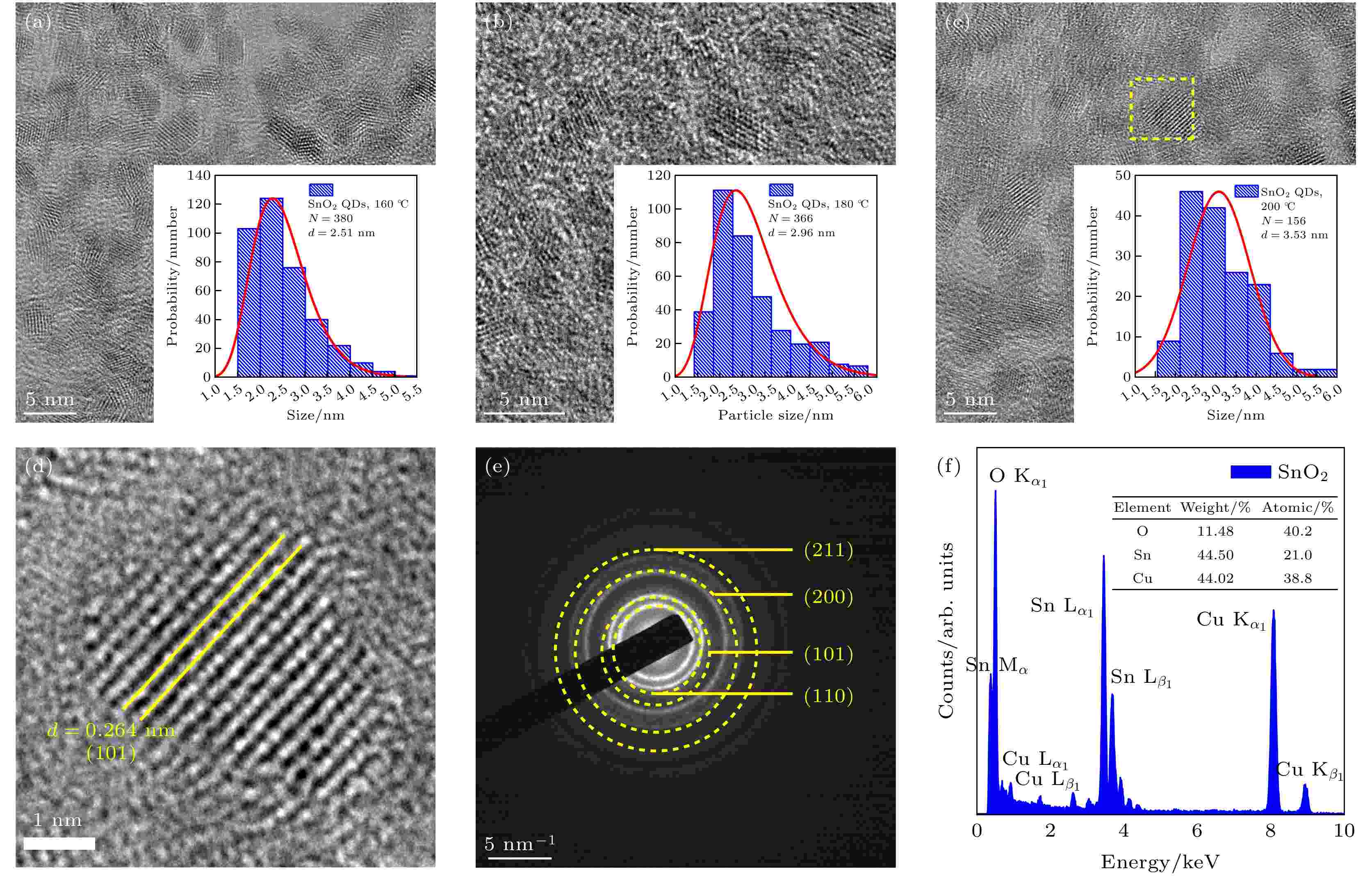
As a non-volatile memory, zero-dimensional quantum dot resistive random access memory (RRAM) has shown broad application prospects in the field of intelligent electronic devices due to its advantages of simple structure, low switching voltage, fast response speed, high storage density, and low power consumption. Tin dioxide quantum dots (SnO2 QDs) are a good option for resistive functional materials with excellent physical and chemical stabilities, high electron mobilities, and adjustable energy band structures. In this paper, the SnO2 QDs with sizes of 2.51 nm, 2.96 nm and 3.53 nm are prepared by the solvothermal method, and the quantum size effect is observed in a small size range and the effective regulation of resistive switching voltage is achieved based on its quantum size effect, which is the unique advantage of quantum dot material in comparison with that of bulk material. Research result shows that as the size of SnO2 QD increases, the SET/RESET voltage gradually decreases from –3.18 V/4.35 V to –2.02 V/3.08 V. The 3.53 nm SnO2 QDs have lower SET/RESET voltage (–2.02 V/3.08 V) and larger resistive switching ratio (> 104), and the resistive switching performance of the device has changed less than 5% after having experienced durability tests 2 × 10⁴ times, showing good stability and retention. Besides, according to the fitting of charge transport mechanism, SnO2 QD RRAM exhibits Ohmic conduction under LRS, while Ohmic conduction, thermionic emission and space charge limit current work together during HRS. The resistive switching effect of SnO2 QDs is controlled by trap filled limit current and interface Schottky Barrier modulation; the trapping/de-trapping behavior of internal defect potential well of SnO2 QDs on electrons dominates the HRS/LRS switching, while the effective control of ITO/SnO2 QDs and SnO2 QDs/Au interface Schottky barrier is the key to accurately regulating the switching voltage. The reason why SnO2 QD RRAM exhibits good size-switching voltage dependence is that the larger SnO2 QD has lower Fermi level and interface Schottky barrier height, so the junction resistance voltage division is reduced, and the SET/RESET voltage decrease accordingly. This work reveals the huge application potential and commercial application value of SnO2 QDs in the field of resistive switching memory, and provides a new option for the development of RRAM.
EDITOR'S SUGGESTION
2021, 70 (19): 197401.
doi: 10.7498/aps.70.20210620
Abstract +
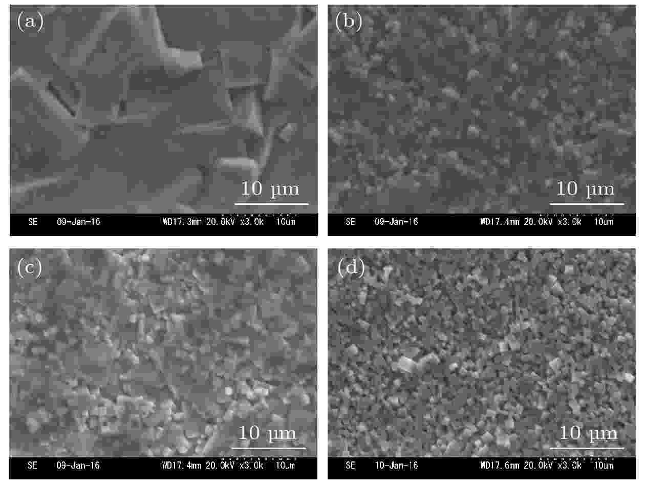
Mg(BH4)2 was previously studied as a promising hydrogen storage material, because of its high gravimetric storage capacities for hydrogen and suitable thermodynamic properties. Mg(BH4)2 began to decompose at about 300 ℃, and formed MgB2 at the end of hydrogen desorption process with the weight content of 14.9% of hydrogen lost. Aside from the prominent hydrogen storage property, the decomposition process from Mg(BH4)2 to MgB2 can be a potential method for fabricating superconducting MgB2 at a low sintering temperature. In this paper, MgB2 bulk was prepared by an in-situ reaction, using the Mg(BH4)2 pressed block as a precursor. The resistance change of the sample was monitored during the Mg(BH4)2 decomposition process and the resistance-temperature (R-T) curve of this process was recorded. Phase of MgH2, Mg and B were formed as the block slowly release its hydrogen before MgB2 occurred. According to the R-T curve, the phase formation of MgB2 started in a relatively low temperature of 410 ℃. Because MgB2 was critically formed by Mg and B derived from Mg(BH4)2, we can compare our formation temperature with previous study on MgB2 prepared by Mg and B in different particle size. The fitting result indicated that the particle size of Mg and B harvest from Mg(BH4)2 decomposition was only 3.4 nm on average. The nearly atomic level mixture of Mg and B resulted in a high chemical reactivity, which was the main reason for low sintering temperature. X-ray diffraction results showed that the purity of MgB2 was 95.2%, and the size of MgB2 grains was 10–18 nm. SEM images showed that the MgB2 bulk had a porous structure and poor connectivity, which was caused by large amount the hydrogen release during the decomposition. MgB2 nanofibers can also be observed inside the bulk. In the superconductivity test, the superconducting transition temperature of the bulk was 35 K. After all, such in situ method to fabricate MgB2 showed a great advantage in some aspects, as its low-cost precursors, low sintering temperature, small grain-size and high superconducting transition temperature in the formed MgB2, which have the potential in industrial scale fabrication of MgB2 bulks and wires.

2021, 70 (19): 197501.
doi: 10.7498/aps.70.20210631
Abstract +


2021, 70 (19): 197502.
doi: 10.7498/aps.70.20210623
Abstract +
In this paper, based on three-dimensional micromagnetic numerical simulation, the influences of the interface layer formed by the atomic diffusion at the interface on magnetic properties in parallel SmCo/Fe bilayer and perpendicular SmCo/Fe bilayer are investigated. For the parallel system, whose nucleation occurs in the second quadrant, as the interface layer thickness increases, the nucleation field and the pinning field increase gradually though the remanence decreases gradually, hence the maximum energy product first goes up and then comes down. As a result, in the system there occurs the transition from the exchange-spring to the rigid magnet. For the perpendicular system, with the increase of the interface layer thickness, a gradual transition from the first quadrant to the second quadrant happens to its nucleation. Although the pinning field experiences the changes from decreasing to unchanging and to increasing, the nucleation field and remanence both rise gradually. Therefore, the energy product is enhanced gradually. During the demagnetization, there appears a spin deviation within the film plane: the parallel system shows a progress of generation and disappearance of the flower and C states; however, the perpendicular system shows a progress of generation and disappearance of the vortex state. With the increase of the ratio of the SmCo atomic diffusion in the interface layer of parallel SmCo/Fe bilayers, the nucleation and pinning field go up, but the remanence decreases, and hence the maximum energy product first rises and then drops. For the two easy axis orientations and any interface layer thickness, the nucleation field rises with the increase of interface exchange energy constant, indicating that the existence of an interface layer between the soft layer and hard layer enhances the exchange coupling interaction between them. The model in this paper well simulates the relevant experimental results [ 2007 Appl. Phys. Lett. 91 072509 ].
2021, 70 (19): 197701.
doi: 10.7498/aps.70.20210440
Abstract +
Piezoelectric ceramics are mainly used in the electronic fields such as actuators, sensors, etc. However, at present the piezoelectric ceramics widely used are lead-based ceramics, which are detrimental to the environment. Based on the needs of environmental protection and social sustainable development, the research of lead-free piezoelectric ceramics becomes urgent. (K, Na) NbO3 (KNN) lead-free piezoelectric ceramics have attracted much attention due to their high piezoelectric coefficient and Curie temperature. However, temperature stability of ceramics is poor, which limits their applications. In this work, (1–x)(Na0.52K0.48)0.95Li0.05NbO3-xCaZrO3(NKLN-xCZ) ceramics with temperature stability are prepared by two-step synthesis. The effects of CaZrO3 on the phase structure, microstructure and electrical properties of KNN-based ceramics are studied. The results show that the appropriate introduction of CaZrO3 can improve the sintering properties of the samples and obtain dense ceramics. All the samples have typical perovskite structure without impurity. With the increase of CaZrO3, the temperature of orthorhombic(O)-Tetragonal (T) phase transition (TO-T) and Curie temperature (TC) move from high temperature to low temperature, while the transition temperature (TO-R) moves from low temperature to room temperature, and then, tetragonal (T) phase and rhombohedral (R) phase coexist in NKLN-xCZ ceramics as $0.05 \leqslant x \leqslant0.06 $ . When x = 0.05, the ceramics have high Curie temperature (Tc = 373 ℃), and show good piezoelectric and ferroelectric properties (piezoelectric constant d33 = 198 pC/N, planar electromechanical coupling coefficient kp = 39%, εr = 1140, tanδ = 0.034, Pr = 21 μC/cm2, Ec = 18.2 kV/cm) because of the density of ceramics and existence of R-T phase boundary around room temperature. In addition, the relative permittivity of ceramics changes with the increase of frequency, which shows a certain relaxation behavior. The relaxation characteristics can be expressed by the modified Curie-Weiss law (1/εr–1/εr,m) = C(T–Tm)α. With the increase of CZ content, the dispersion coefficient α of ceramics increases (x = 0.07, α = 1.96), which can be ascribed to A-site cation disorder induced by the addition of CZ. The temperature range of phase transition is widened because of the diffused R-T phase transition. Therefore, the ceramics have temperature-stable electrical properties: the kp of NKLN-0.05CZ ceramics is kept at 34%–39% (variation of kp $\leqslant 13\% $ ) in a temperature range of –50–150 ℃. It provides methods and ideas for further exploring the temperature stability of KNN-based ceramics.


2021, 70 (19): 197801.
doi: 10.7498/aps.70.20210122
Abstract +
In the information display field, micro-light-emitting diodes (micro-LEDs) possess high potentials and they are expected to lead the direction of developing the next-generation new display technologies. Their display performances are superior to those produced by the currently prevailing liquid crystal and organic light-emitting diode based technologies. However, the micro-LED pixels and their driving circuits are often fabricated on different wafers, which implies that the so-called mass transfer seems to be inevitable, thus facing an obvious bottleneck. In this paper, the emerging graphene field effect transistors are used as the driving elements and integrated onto the GaN micro-LEDs, which is because the pixels and drivers are prepared directly on the same wafer, the technical problem of mass transfer is fundamentally bypassed. Furthermore, in traditional lithographic process, the ultraviolet photoresist directly contacts the graphene, which introduces severe carrier doping, thereby leading to deteriorated graphene transistor properties. This, not surprisingly, further translates into lower performances of the integrated devices. In the present work, proposed is a technique in which the polymethyl methacrylate (PMMA) thin films act as both the protection layers and the interlayers when optimizing the graphene field effect transistor processing. The PMMA layers are sandwiched between the graphene and the ultraviolet photoresist, which is a brand new device fabrication process. First, the new process is tested in discrete graphene field effect transistors. Compared with those devices that are processed without the PMMA protection thin films, the graphene devices fabricated with the new technology typically show their Dirac point at a gate voltage (Vg) deviation from Vg = 0, that is, 22 V lower than their counterparts. In addition, an increase in the carrier mobility of 32% is also observed. Finally, after applying the newly developed fabrication process to the pixel-and-driver integrated devices, it is found that their performances are improved significantly. With this new technique, the ultraviolet photoresist no longer directly contacts the sensitive graphene channel because of the PMMA protection. The doping effect and the performance dropping are dramatically reduced. The technique is facile and cheap, and it is also applicable to two-dimensional materials besides graphene, such as MoS2 and h-BN. It is hoped that it is of some value for device engineers working in this field.

2021, 70 (19): 197802.
doi: 10.7498/aps.70.20202235
Abstract +

2021, 70 (19): 197901.
doi: 10.7498/aps.70.20210651
Abstract +
As a novel low-cost semiconductor with extraordinary photoelectric property, the inorganic CsPbX3 perovskites have become emerging materials for the next generation of X-ray detectors in the past decade. However, most of recent studies of CsPbX3 perovskite X-ray detectors are based on their internal photoelectric effect. Though it is also important and widely used in vacuum X-ray detectors, the external photoelectric effect of CsPbX3 perovskite has been rarely studied by now. Thus, the response sensitivity of the CsPbX3 perovskite’s external photoelectric effect in the X-ray region is studied in the present paper. First, a 230-nm-thick CsPbI2Br membrane is prepared on a metal substrate by a conventional one-step deposition method, with a precursor solution used. Then the external photoelectric responsivity and quantum efficiency of the CsPbI2Br membrane are calibrated in a range from 2000 to 5500 eV at Beijing Synchrotron Radiation Facility. The responsivity is over 5.1 × 10⁻⁵ A/W in the range and the quantum efficiency is over 23%. These calibration data are close to those of a traditional X-ray photoelectric material CsI. The Monte-Carlo method is utilized to simulate the external photoelectric effect of CsPbI2Br perovskite, and the external photoelectric responsivity is calculated. The calculated data match well with the calibration, proving the Monte-Carlo method feasible for the external photoelectric effect simulation of CsPbX3 perovskite. Then the external photoelectric responsivities and quantum efficiencies of CsPbX3 perovskites are calculated via the Monte-Carlo method in the X-ray range from 2000 to 10000 eV. The calculated responsivities of different CsPbX3 perovskites are all close to the responsivity of CsI, and an order of magnitude higher than that of Au, and the CsPbX3 quantum efficiencies also follow a similar scenario. This indicates that CsPbX3 perovskites have good external photoelectric properties and potential applications in X-ray vacuum detectors such as photocathode and photomultiplier. The influence of thickness on CsPbX3 photoelectric response is also studied in this paper via Monte-Carlo simulation. The results show that the responsivity increases with the material thickness increasing, which is due to the increased X-ray absorption. The responsivities all reach their upper limits at a material thickness of about 150 nm, which means that the electrons generated at 150 nm can hardly escape from the material surface. It is indicated that the thickness of CsPbX3 should be no less than 150 nm to obtain the optimal photoelectric response.
INTERDISCIPLINARY PHYSICS AND RELATED AREAS OF SCIENCE AND TECHNOLOGY
2021, 70 (19): 198101.
doi: 10.7498/aps.70.20210521
Abstract +
Silicon/carbon composite is one of the most potential high-capacity anode materials for lithium-ion batteries. The interface state between silicon and carbon of silicon/carbon composite is an important factor affecting its electrochemical performance. In this paper, Sin (n ≤ 6) clusters with different numbers of Si atoms are constructed on graphene as a structural unit of carbon material. The geometric configuration, structure stability and electronic property of Sin clusters adsorbed on graphene (Sin/Gr) are studied by the first-principles method based on density functional theory (DFT). The results show that when the number of Si atoms n ≤ 4, the Sin clusters are preferentially adsorbed on graphene in a two-dimensional configuration parallel to graphene. When n ≥ 5, the Sin clusters are preferentially adsorbed on graphene in a three-dimensional configuration. With the increase of the number of Si atoms n, the thermodynamic stability of Sin clusters on graphene decreases significantly, the interface binding strength between Sin clusters and graphene decreases, and the charge transfer between Sin clusters and graphene becomes less. At the same time, the storage capacity of Li atoms in Sin/Gr complex is also studied. Li atoms are mainly stored on the graphene surface near Sin clusters and around Sin clusters. The complex synergistic effect of Sin clusters and graphene enhances the thermodynamic stability of Li adsorption. When n ≤ 4, storing two Li atoms is beneficial to improving the thermodynamic stability of xLi-Sin/Gr system, and the thermodynamic stability decreases with the increase of Li atom number. When n ≥ 5, the thermodynamic stability of xLi-Sin/Gr system decreases with the increase of Li atom number. In the xLi-Si5/Gr system, the C-C bond and Si-Si bond are mainly covalent bonds, while the Li-C bond and Li-Si bond are mainly ionic bonds with certain covalent properties.

2021, 70 (19): 198401.
doi: 10.7498/aps.70.20210681
Abstract +
Orbital angular momentum, as a basic physical quantity of electromagnetic waves, has been widely studied since 1992. Recently, the geometric phase metasurface, which is also known as Pancharatnam-Berry (P-B) phase metasurface, has been proposed. Because of its frequency-independent and angle-dependent phase control characteristics, it can generate high-performance and broadband vortex wave. However, the current design of reflective metasurface encounters the following problems: 1) the reflected vortex wave is partly blocked by the feeding antenna; 2) in practical applications, the cross-polarized field will inevitably be induced due to the feed antenna and the reflective metasurface. How to avoid the cross-polarization is still worth further investigating. In this work, an offset-fed vortex wave generator is proposed. It consists of a right-handed circularly polarized Archimedes spiral antenna and a reflective metasurface. Firstly, the offset feeding design is introduced to avoid generating the cross-polarized fields caused by the feeding antenna. A geometric meta-atom of the reflective metasurface is designed at a working frequency of 8.5 GHz. By regularly arranging meta-atoms with different orientation angles, the convergence and phase compensation functions are imparted only to the co-polarization field. The cross-polarized field is intentionally weakened and refracted along other directions. Subsequently, a low cross-polarized vortex wave with an enhancement effect is obtained at the desired observation position. There are three contributions made in this work: 1) a P-B meta-atom is proposed to fabricate the reflective metasurface; 2) the conversion relationship between the co-polarized and cross-polarized field is studied from the initial state to the final state, and the four transformation processes are demonstrated in detail; 3) an offset-fed vortex wave generator is established which allows one to generate high-performance vortex beam with arbitrary OAM mode. The experimental results are in good agreement with those simulation results, proving the proposed method effective and feasible. The proposed design shows its advantages including simple structure, polarization selectivity, and regional field enhancement effect, which has great potential applications in vortex wave communication and OAM-based target detection.

2021, 70 (19): 198402.
doi: 10.7498/aps.70.20210205
Abstract +
2021, 70 (19): 198403.
doi: 10.7498/aps.70.20210586
Abstract +
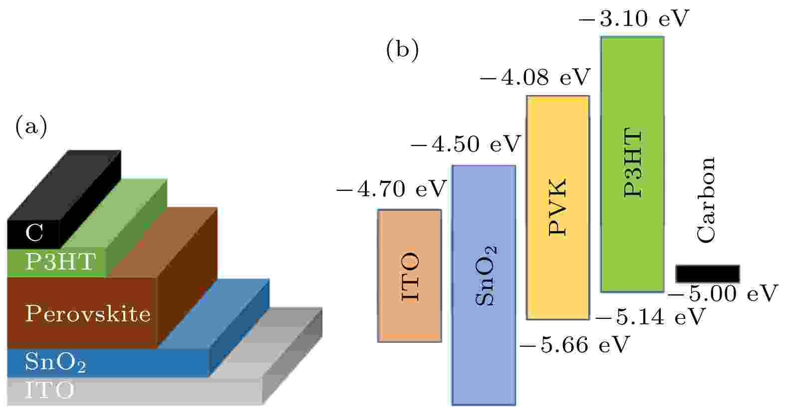
HTL-free carbon-based perovskite solar (PSCs) batteries have the advantages of low cost, simple preparation steps, and high stability, and have broad application prospects. However, the direct contact between the carbon electrode and the active layer causes the photoelectric conversion efficiency of the device to be generally lower than that of other metal electrode perovskite solar cells. Therefore, it is necessary to add a hole-transport layer between the perovskite layer and the electrode to improve the charge transport efficiency and optimize the performance. Poly(3-hexylthiophene) has excellent photoelectric properties and is regarded as one of the suitable hole transport materials for perovskite solar cells. In this paper, P3HT is used as the hole transport layer of the device. Compared with the traditional organic hole-transport layer Spiro-OMeTAD, the P3HT has the advantages of low cost and easy manufacture. However, in the current devices with using P3HT as the hole transport layer, due to the characteristics of the surface morphology and molecular ordering of the P3HT film, the carrier mobility in the film itself is low, resulting in unsatisfactory device performance. Studies have shown that the surface morphology and molecular arrangement of the P3HT film can be changed by doping, and the migration rate of charge-carriers inside the film can be accelerated, thereby improving the photovoltaic performance of the solar cell. In this paper, a printing process is used to print carbon paste on the hole transport layer as the electrode of the device, and spin coating is used to prepare the transport layer. And through the method of doping 1,8-diiodooctane (DIO) in P3HT to optimize the device performance, the photoelectric conversion efficiency of the carbon-based perovskite solar cell is improved, the mobility of holes is improved, and the transportation of electrons is blocked. The reduced interface recombination, the improved interface contact between the carbon electrode and the device, the increased short-circuit current Jsc and the fill factor FF lead the photoelectric conversion efficiency of the device to increase from 14.06% to 15.11%. We test the light stability of the device under the 1000-h continuous illumination in a nitrogen atmosphere, and the conversion efficiency of the device remains above 98%, indicating that the addition of DIO into P3HT improves not only the photoelectric conversion efficiency of the device, but also the stability.
EDITOR'S SUGGESTION
2021, 70 (19): 198404.
doi: 10.7498/aps.70.20211037
Abstract +
The back electrode is an important factor affecting the performance of perovskite solar cells. In this paper, the effects of back electrode material, structure and thickness on the performance of perovskite solar cells are studied by using COMSOL software. It is found that compared with the work function of the back electrode metal, its resistance has small effect on solar cell performance. Besides the back electrode structures affecting cell performance, there are other factors affecting cell performance. In terms of the back electrodes with honeycomb structure, considering the difficulty in fabricating, the best cost performance occurs when the radius of the circle is approximately equal to the edge spacing. It is predicted that the cell performance will be improved by about 5% in porosity with increasing 10% in the back electrode. The resistance of the back electrode decreases with its thickness increasing. Considering the process and cost, the optimal thickness should be between 100 nm and 150 nm.
EDITOR'S SUGGESTION
2021, 70 (19): 198502.
doi: 10.7498/aps.70.20211046
Abstract +
Metal halide perovskite light-emitting diodes have attracted much attention due to their excellent characteristics such as low-cost solution-processing, high luminous efficiency and excellent color purity. However, low luminous efficiency and spectrum stability of blue perovskite light-emitting device restrict the further development of perovskite materials in the field of displays and lighting. Here in this work, we study the effects of ammonium thiocyanate (NH4SCN) addition on the morphology, crystal structure, photo-physics, charge transport and electroluminescence properties of quasi-two-dimensional mixed-halide perovskite films by measuring scanning electron microscope (SEM), X-ray diffraction (XRD), UV-Vis spectrum, steady-state photoluminescence (PL), and transient PL and analyzing the current density–voltage characteristics of hole-dominated device and current density-voltage-luminance plots of light-emitting device. The results indicate that ammonium thiocyanate (NH4SCN) can effectively passivate the defects, improve the crystallinity, and modulate the phase distribution of quasi-two-dimensional mixed-halide perovskite film, thereby increasing charge transport and luminescent efficiency. Notably, PL intensity of the 20%-NH4SCN sample is 1.7 times higher than that of the control sample, which is attributed to the defect passivation effect of NH4SCN probably due to the Lewis acid-base interaction with Pb2+. Meanwhile, the hole mobility of the 20%-NH4SCN sample is measured to be 1.31 × 10⁻⁵ cm2/(V·s), which is much higher than that of the control sample (3.58 × 10⁻⁶ cm2/(V·s)). As a result, sky-blue quasi-two-dimensional mixed-halide perovskite light-emitting diode with 20%-NH4SCN possesses an EL maximum at 486 nm and a maximum external quantum efficiency (EQE) of 5.83% and a luminance of 1258 cd/m2, which are 6.7 and 3.6 times higher than those of the control device without NH4SCN, respectively. At the same time, the EL spectra of the 20%-NH4SCN device are barely changed under different operating voltages, whereas the EL spectra of the control device show a 7–10 nm red-shift under the same condition, indicating that the NH4SCN addition inhibits halide phase separation and improves the EL spectrum stability. In addition, the T50 operational life-time of the 20%-NH4SCN device is measured to be about 110 s, which is superior to that of the control device (39 s) due to improved film quality of NH4SCN-modified sample. This research provides a simple and effective method to improve the performances of quasi-two-dimensional mixed-halide perovskite blue-emitting diodes.
2021, 70 (19): 198503.
doi: 10.7498/aps.70.20210242
Abstract +
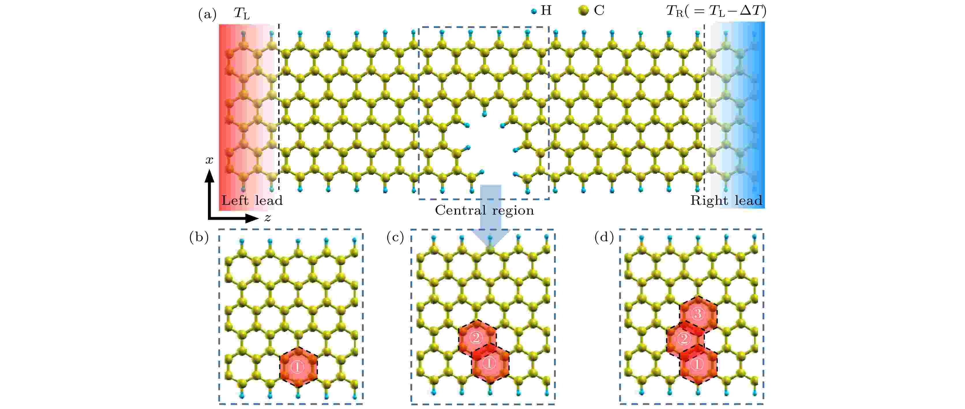
Spin caloritronics, which combines the characteristics of thermoelectronics with the characteristics of spintronics, has a wide range of promising applications in high-speed and low-dissipation devices. In this paper, according to the density functional theory combined with nonequilibrium Green’s function method, we propose a scheme for generating pure spin current with spin dependent Seebeck effect in the zigzag-edged graphene nanoribbons by introducing continuous antidots (hexagonal defects). Specifically, by creating an antidot at one edge of the nanoribbon, an X-shape transmission spectrum around the Fermi level is formed, which results from the disrupted edge of the nanoribbon. The mechanism is well explained by the cooperation between the varying localization features of the eigenstates around the Fermi level for the unit cell and the scattering states at the Fermi level for the device. Therefore, the electrons of the two spin channels flow in the opposite directions under a temperature gradient, generating the spin current and charge current. By slightly tuning the chemical potential of the device, the charge current can be zero, while the spin current is not equal to zero. With the increase of adjacent antidot number along the width of the nanoribbons, the structures are more disrupted, thus promoting the pure spin current due to the increase of the spin Seebeck coefficient. However, for zigzag graphene nanoribbons with W zigzag carbon chains, the pure spin current decreases when the number of the antidots are more than (W/2–1), which results from the decrease of the spin conductance. So, the maximum pure spin current can be obtained when the number of the continuous antidots introduced along the width of nanoribbons reaches (W/2–1). These findings indicate a novel strategy for thermally generating the spin current by introducing continuous antidots along the nanoribbon bandwidth in zigzag graphene nanoribbons and will be greatly instructive in designing the graphene spintronic devices.
EDITOR'S SUGGESTION
2021, 70 (19): 198701.
doi: 10.7498/aps.70.20210941
Abstract +
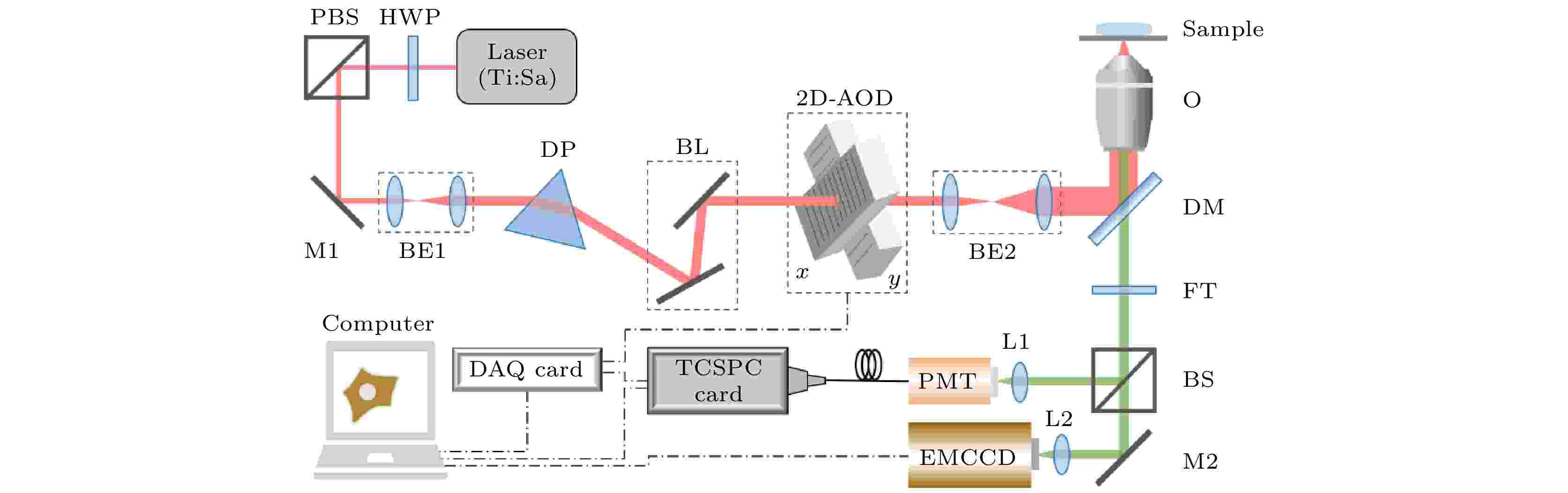
Fluorescence lifetime imaging microscopy (FLIM) has been widely used in biomedical research due to its high specificity, high sensitivity and quantification ability in cell microenvironment sensing. The fluorescence lifetime detection method based on time-correlated single photon counting (TCSPC) is one of the most commonly used techniques at present. However, due to the limitation of imaging principles and conditions, this technique has the disadvantages of long data acquisition time and consequently low imaging speed. In this paper, a fast FLIM technique for any number of discrete and irregular regions of interest (ROIs) in biological samples is developed. The technology uses acousto-optic deflectors (AODs) to achieve fast and flexible addressing scanning, optimize the synchronization strategy between AOD and TCSPC, and reconstruct the lifetime image through simple online feature analysis of the ROI shapes. For the case of multiple discrete irregular ROIs in biological samples, it can greatly save the time of data acquisition, thus realizing the fast FLIM imaging of these ROIs, which is benificial to the study of the heterogeneity of biological events in biological system. In particular, the fast fluorescence imaging result for 87 discrete points in the field of view shows that this method can obtain a fluorescence lifetime image in a very short acquisition time (only 52.2 ms) and thus achieving a very fast imaging speed in such a situation. Dynamic FLIM imaging of lysosome probe LysoSensor Green DND-189 in living cells stimulated by ammonium chloride is carried out to monitor the real-time change of pH value in lysosome lumen. The acquisition time for a single fluorescence lifetime image of lysosomes in two ROIs is only 200 ms. The results show that the rapid FLIM technology can be used to dynamically monitor the changes of microenvironment in biological samples, and will play an important role in the microenvironment sensing in living cells.
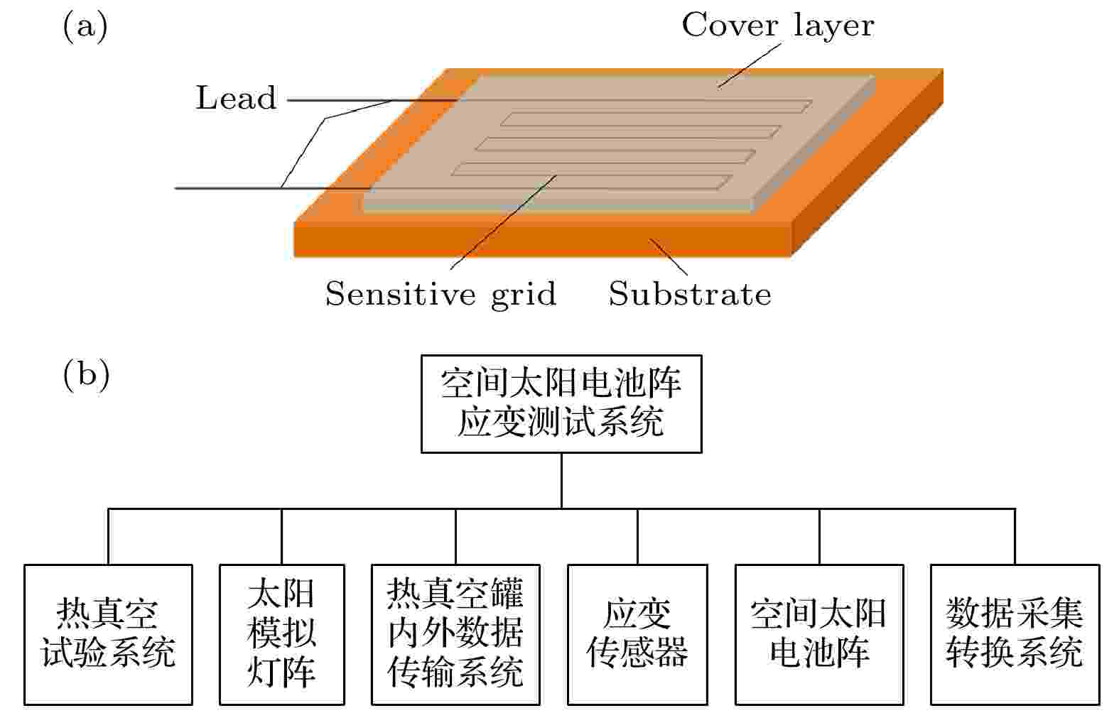
2021, 70 (19): 198801.
doi: 10.7498/aps.70.20210320
Abstract +
Space solar cell array is the only power source for satellites, and the mechanical impact on solar array during its in-orbit service will directly affect the normal operation of the satellites. Therefore, it is of great significance to study the stress and strain law of space solar array. In this paper, we establish a strain-testing system for space solar array, and this system can help test the strain data of space solar array under simulated space vacuum and thermal cycling field. We find that the space solar cells suffer compression deformation at high temperature and tensile deformation at low temperature. The total maximum strain of the free cell and pasted cell under the same conditions are 1270 and 1320 με, respectively. In addition, the strain of middle area is 113% higher than that of the edge area in one space solar cell. The rupturing strain of space solar cell is 2080 με. These measured data conduce to studying the deformation characteristics of solar cells in space environment, which can help researchers get the deformation regularity of space solar cells. They also provide experimental basis for stress-relieving arrangement of space solar array. This research provides technical support for studying the deformation resistance of space solar cells.
GEOPHYSICS, ASTRONOMY, AND ASTROPHYSICS

2021, 70 (19): 199201.
doi: 10.7498/aps.70.20210283
Abstract +
Twelve lightning flashes are successfully triggered under the positive atmospheric electric field condition. The discharge properties of the flashes, and the propagation characteristics and mechanism of the involving upward negative leaders are investigated. When lightning flashes are triggered, the average ground atmospheric electric field is around 5 kV/m, with a maximum value exceeding 13 kV/m. Except for one special event showing a discharge polarity reversal (from positive to negative) and producing multiple negative return strokes, none of the remaining 11 triggered lightning flashes involves the subsequent return stroke process. The discharge currents of these flashes are generally of the order of several hundred amperes. The successfully triggered lightning flashes start with the initiation and the upward propagation of negative stepped leaders, of which the average two-dimensional velocity is 1.85 × 10⁵ m/s. For a total of 132 steps captured by the high-speed video camera, the step lengths range from 0.8 m to 8.7 m, with an average of 3.9 m. During the initial stage of the upward negative stepped leader, the current and electromagnetic field present a significant impulsive feature. The mean value of pulse interval, current peak, charge transfer, half-peak-width and current rise time T10%–90% are 17.9 μs, 81A, 364 μC, 3.1 μs, and 0.9 μs, respectively. The equivalent linear charge density of a single step is 118.5 μC/m. The branching of the leader channel generally takes place together with the stepping process in two ways: the first way is to implement the multiple connections of clustering space stems/space leaders to the leader head within an individual step cycle, and the corresponding current waveform presents a multi-peak structure, with a peak interval of about 2–3 μs (up to 6–7 μs); the second way is to reactivate those previously extinguished space stems/space leaders and to connect them to the lateral surface of the channel.
2021, 70 (19): 199301.
doi: 10.7498/aps.70.20210632
Abstract +
A large high altitude air shower observatory (LHAASO) located at Daocheng in Sichuan province, China, with an altitude up to 4410 m above the sea level, takes the function of hybrid technology to detect cosmic rays. It is composed of three sub-arrays: a 1.3 km2 ground-based particle detector array (KM2A) for γ-ray astronomy and cosmic ray physics, a 78000 m2 water Cherenkov detector array (WCDA) for γ-ray astronomy, and 18 wide field-of-view air Cherenkov/fluorescence telescopes array (WFCTA) for cosmic ray physics. As the major array of LHAASO, KM2A is composed of 5195 electromagnetic particle detectors (EDs, each with 1 m2) and 1188 muon detectors (MDs, each with 36 m2). In the ground-based experiments, there are two common independent data acquisition systems, corresponding to the shower and scaler operation modes. Up to now, the KM2A array operates only in shower mode with the primary energy threshold of about 10 TeV. In the scaler mode, it is not necessary for too many detectors to be hit at the same time. The energy threshold of the experiment can be greatly lowered. In order to learn more about the scaler mode in LHAASO-KM2A, we adopt the CORSIKA 7.5700 to study the cascade processes of extensive air showers in the atmosphere, and employ the G4KM2A (based on Geant4) to simulate the detector responses. The KM2A-ED array is divided into dozens of clusters. For one cluster (composed of 64 EDs), the event rates of showers having a number of fired EDs ≥ 1, 2, 3, 4 (in a time coincidence of 100 ns) are recorded. The average rates of the four multiplicities are ~88 kHz, ~1400 Hz, ~220 Hz, and ~110 Hz, respectively. The particle multiplicities m ≥ 3 are almost completely due to cosmic ray secondary particles. The corresponding primary energies and effective areas are also given in this paper. According to our simulations, the energy threshold of the scaler mode can be lowered to 100 GeV, and the effective areas reach up to ~100 m2. The simulation results in this work are helpful in the online triggering with the scaler mode, and provide information for the subsequent data analysis in LHAASO-KM2A.
