Search

Article

x
Special topic

更多 
Topics
Article Type

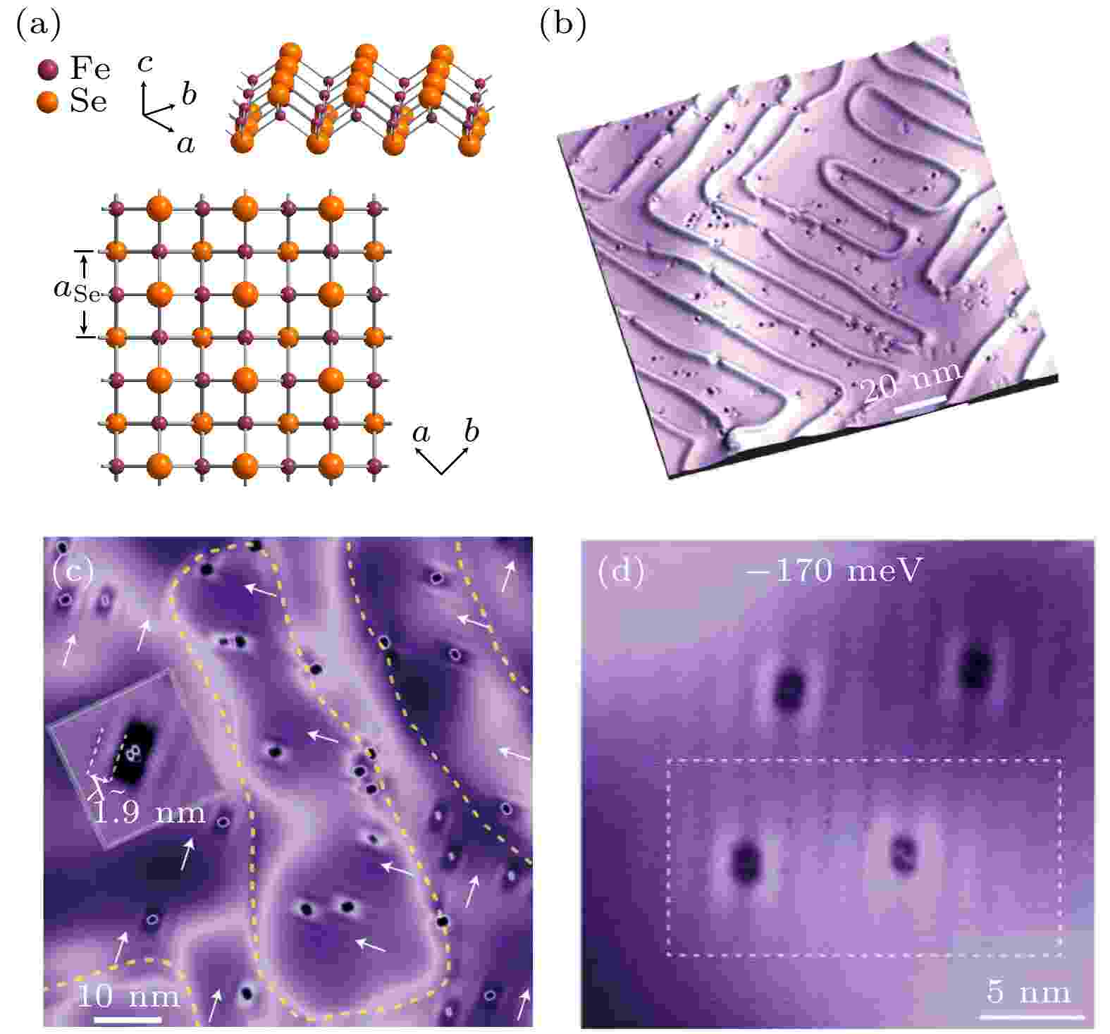
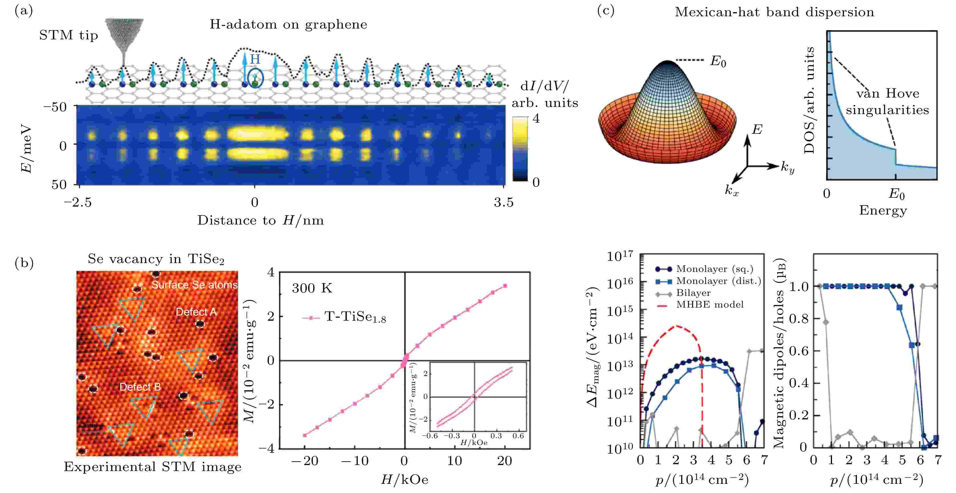
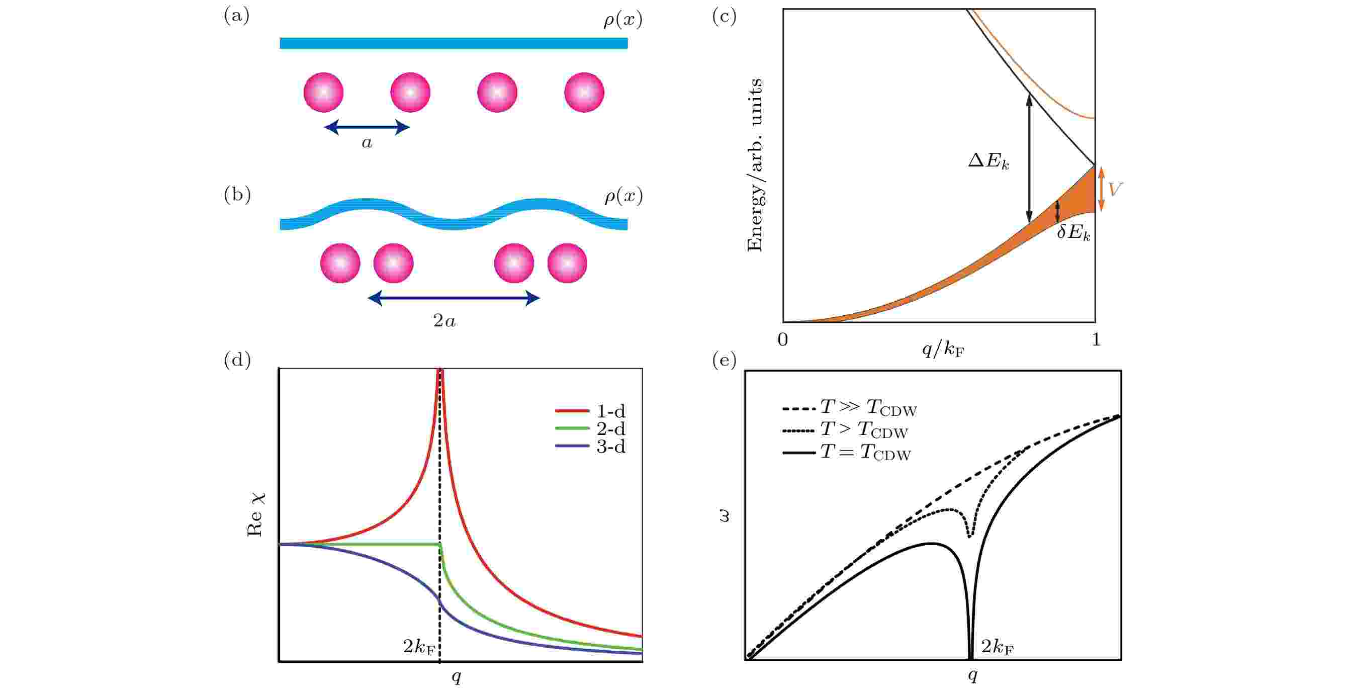
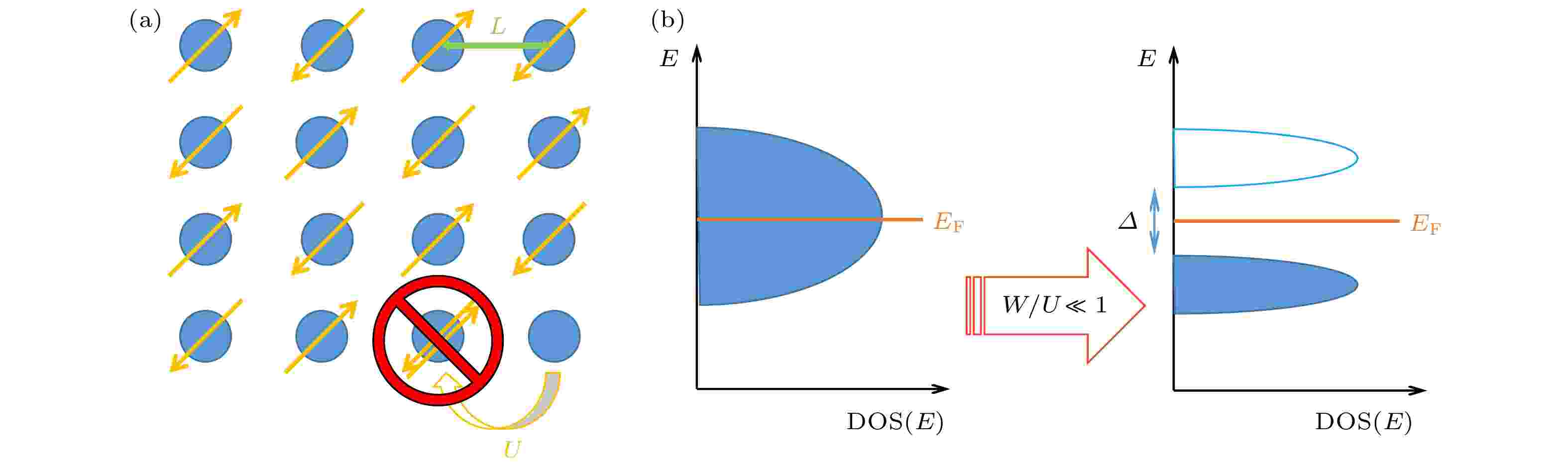
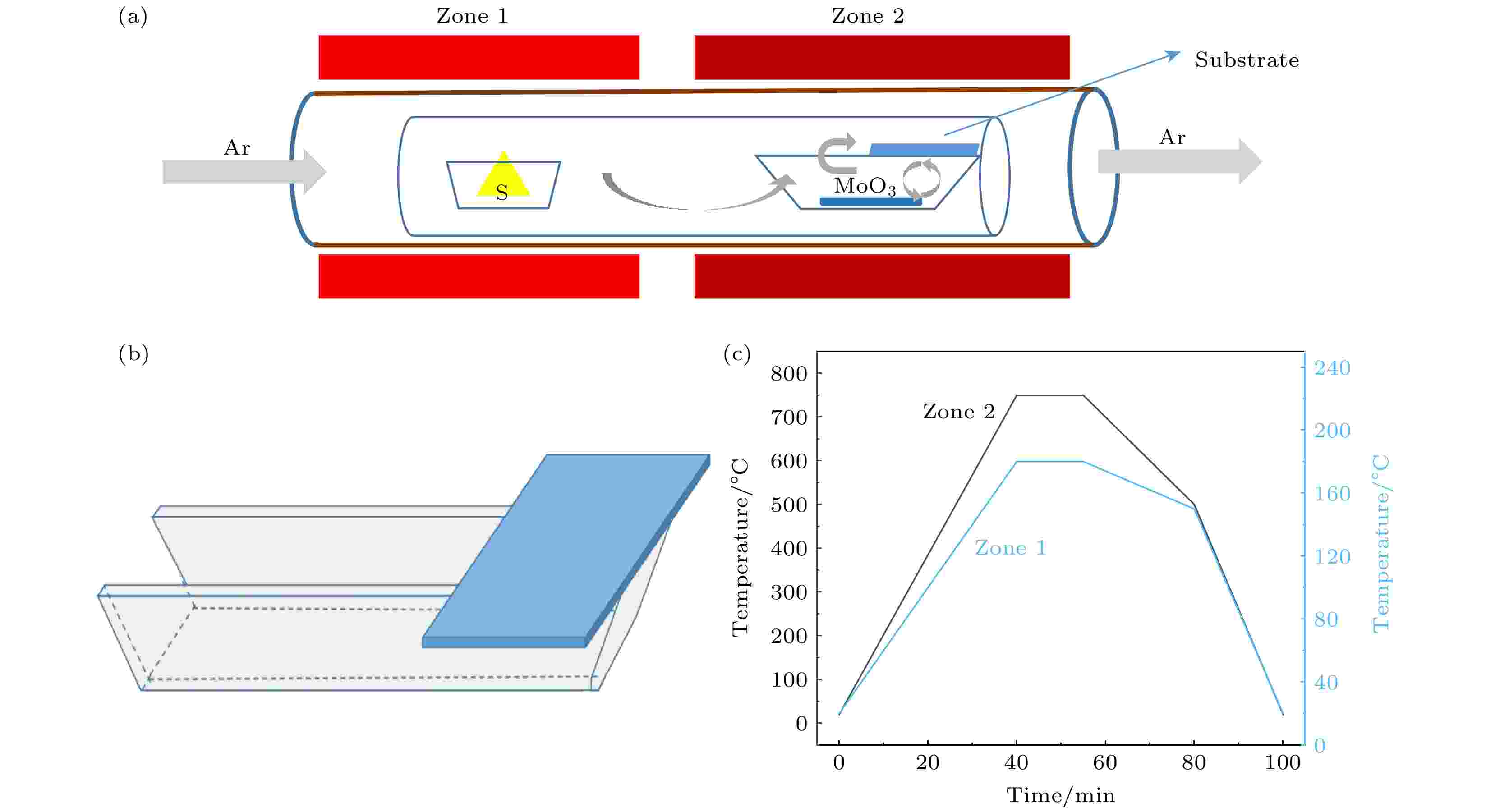
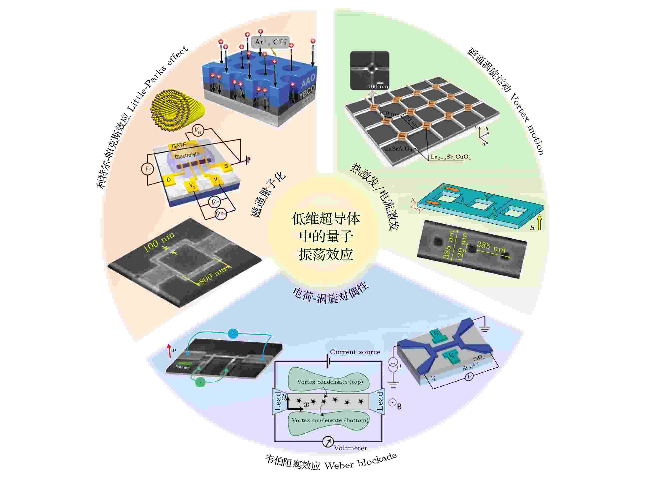
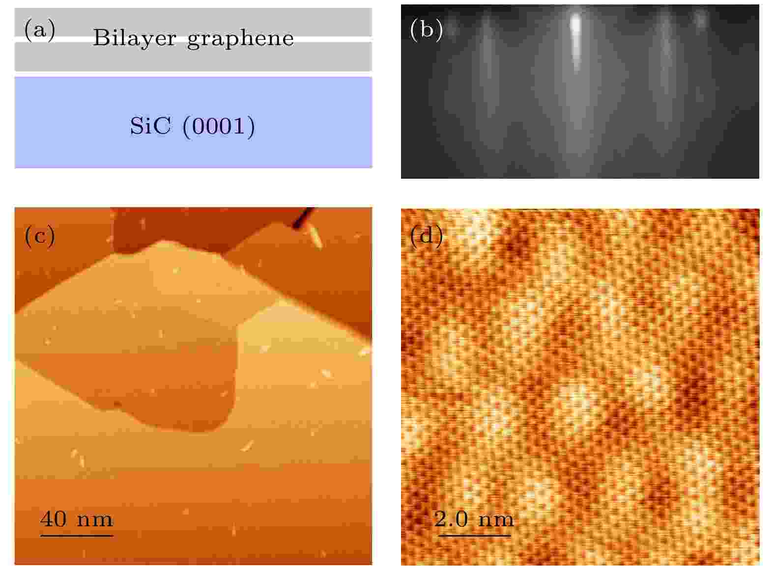
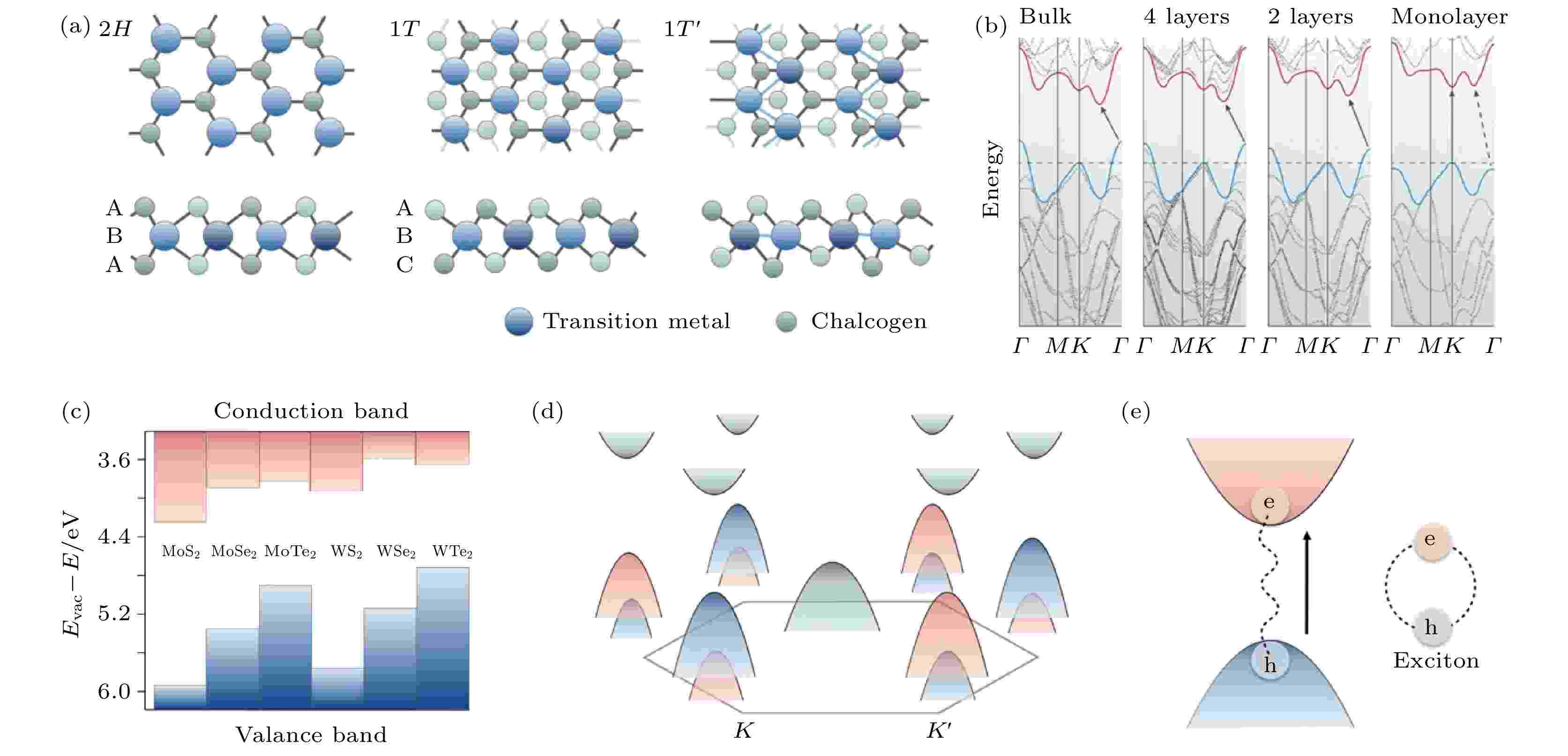
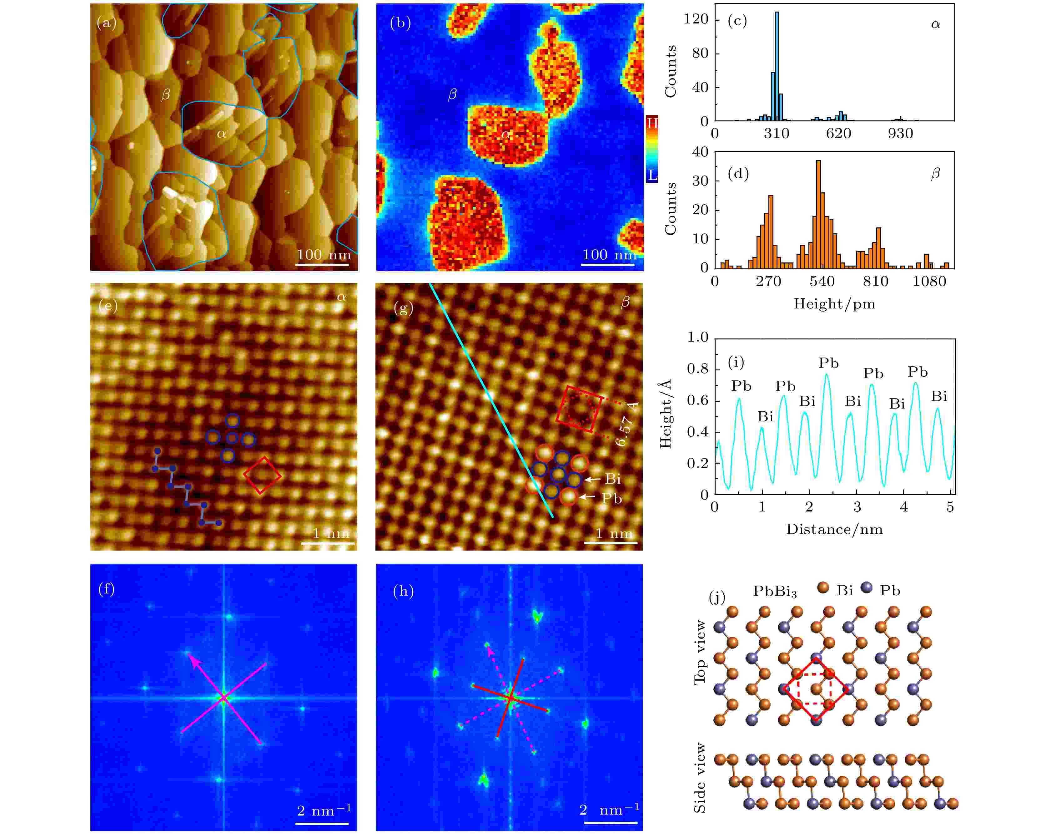
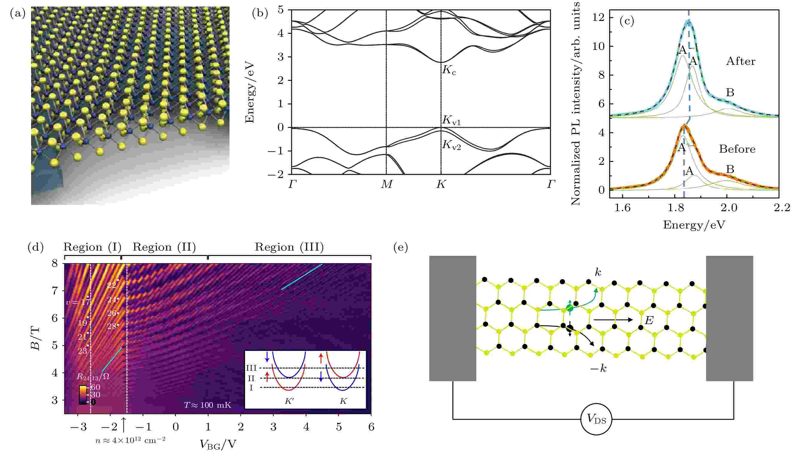
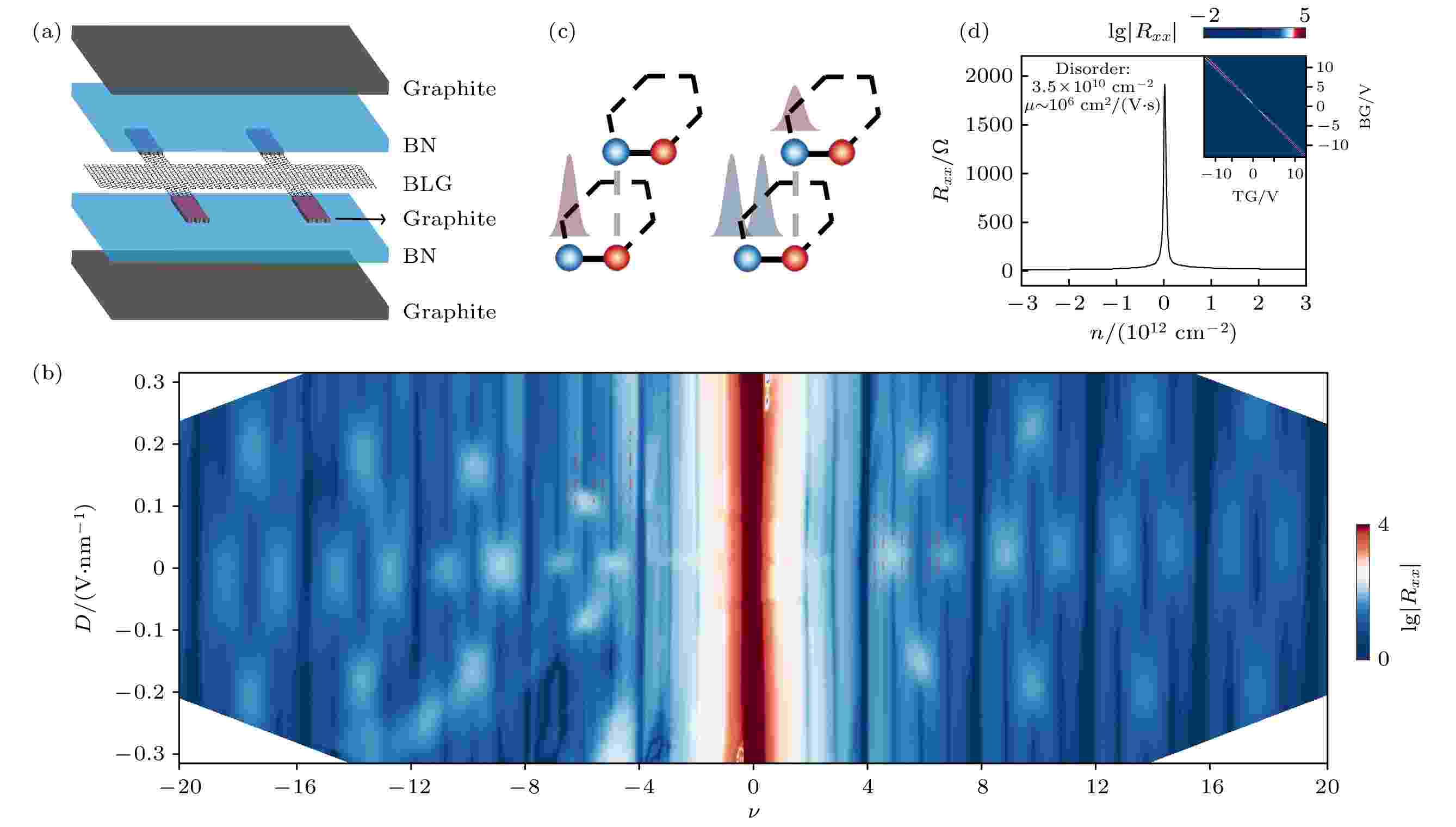
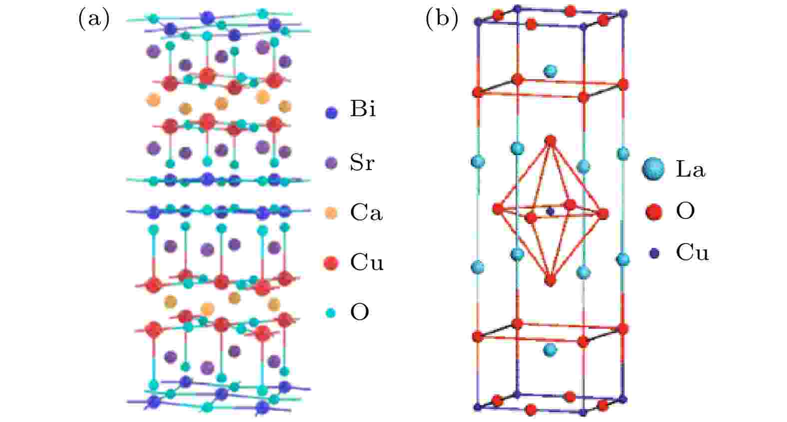
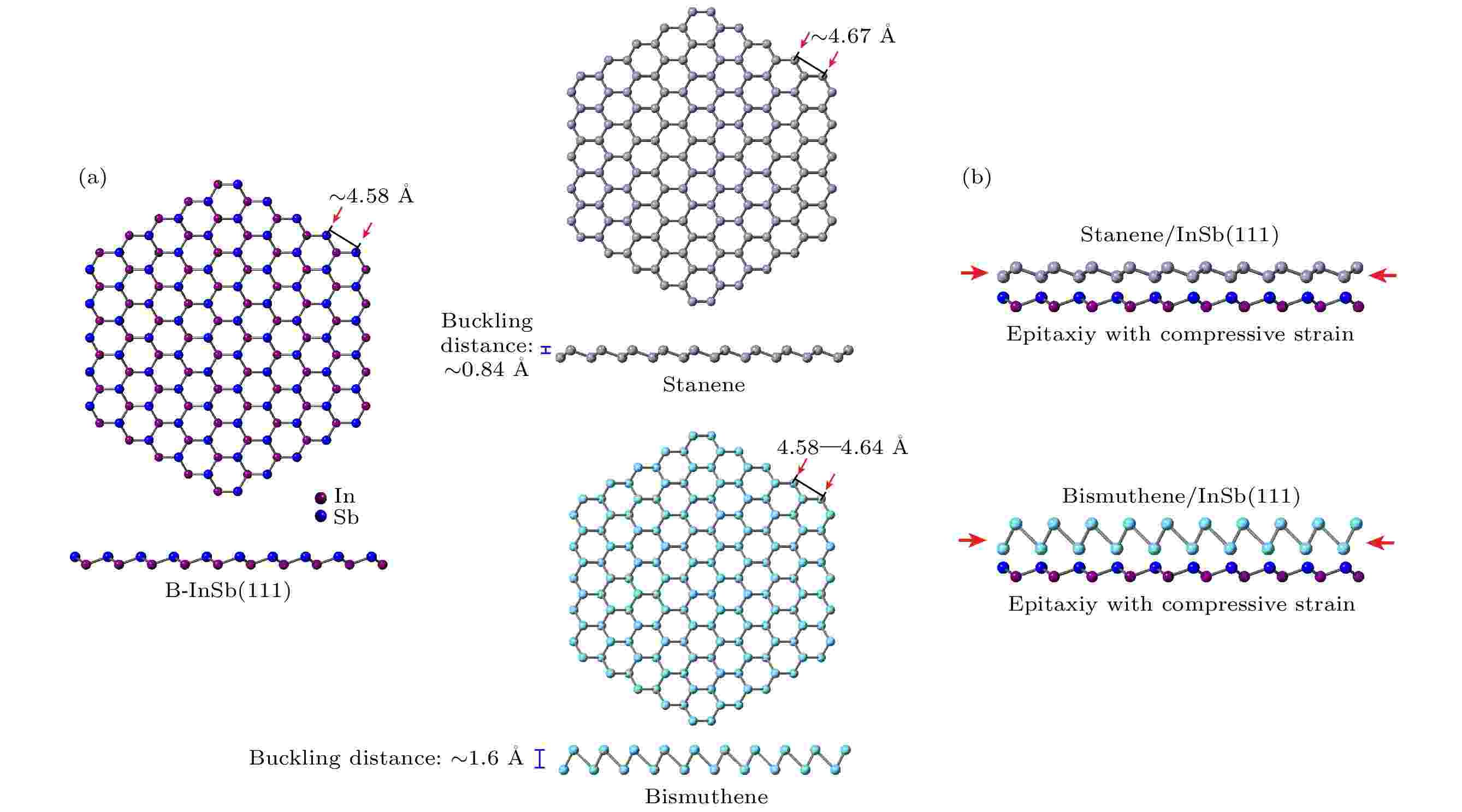
Novel properties of low-dimensional materials

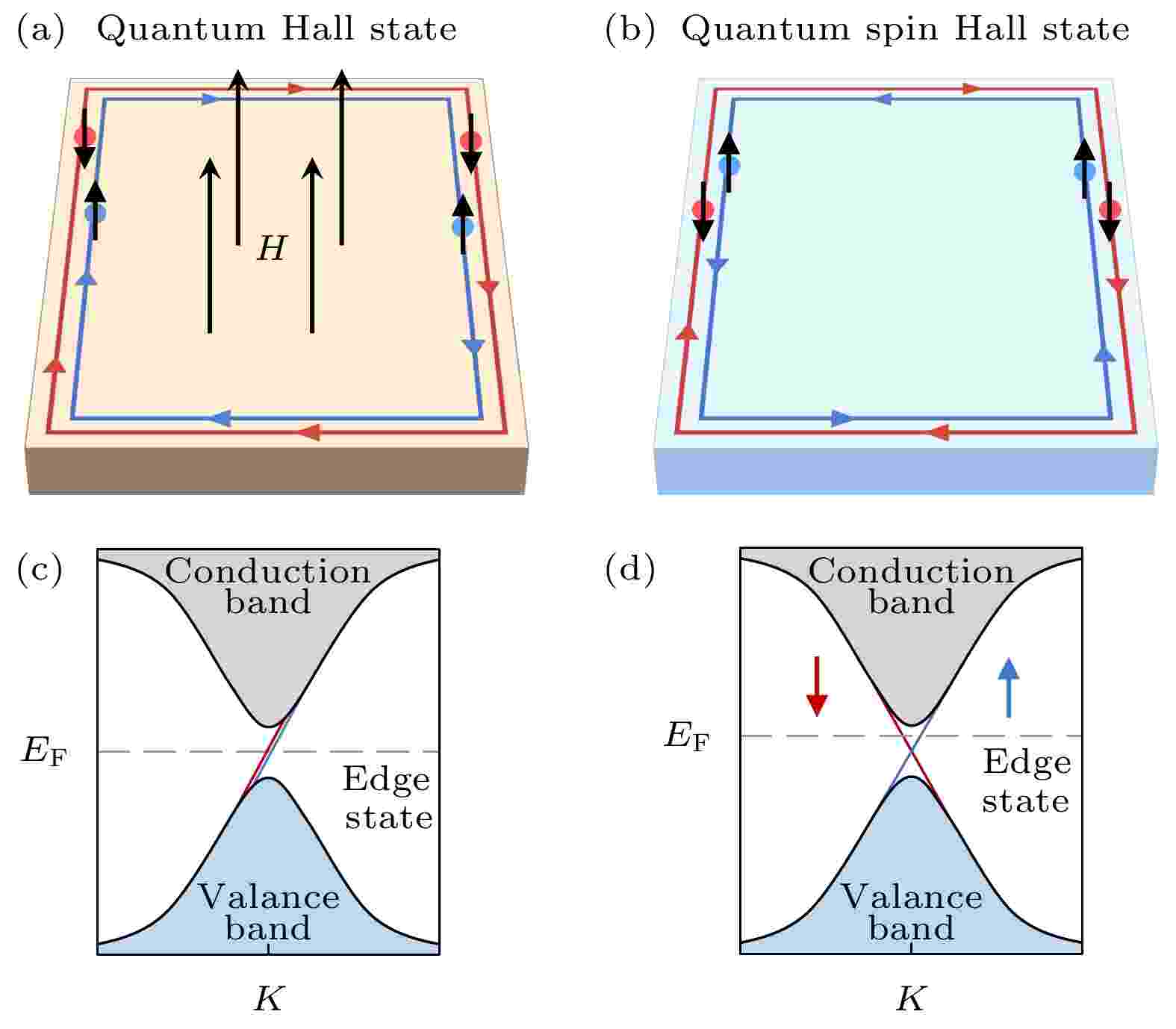
       纵观历史, 人类对材料的认知不断推动着社会的进步和发展, 这方面在过去一个多世纪对材料电学性质的研究上体现得尤为显著. 我们可以将材料粗略地分为金属、半导体、绝缘体, 也可以分为超导、非超导、磁性、非磁性等. 不难发现, 所有这些性质都源于同一种微观粒子: 电子. 随着研究的深入, 科学家们开始期待在一种材料中能实现以上多种甚至所有可能的电子态. 最近, 以二维体系为代表的低维体系研究向我们展示了实现这一愿景的可能性. 在低维体系中, 维度的降低导致体系对载流子浓度、介电环境、压强、应力、电场、磁场等非常敏感. 因此, 我们可以在一个极其宽广的多参数空间对其结构和物性进行精细调控, 进而实现一系列新奇量子物态. 例如在魔角双层石墨烯中就可实现金属/关联绝缘态, 非超导/超导, 非磁性/磁性, 甚至量子反常霍尔效应等多种新奇物态.一方面, 基于低维体系的这些研究极大地推进了人们对凝聚态物理中各种新奇量子物态、相变以及准粒子关联等问题的深入理解; 另一方面, 低维体系高度可调的特点也为其在未来的应用提供更广阔的空间. 值得一提的是, 低维材料的一个显著优势是其新奇物态都直接暴露在材料表面, 这为直接观测这些量子物态提供了一个前所未有的机会. 最近, 科学家们利用扫描隧道显微镜成功地实现了对石墨烯中的量子霍尔铁磁态、双层石墨烯畴界的谷极化导电通道、拓扑绝缘体中的拓扑边界态的直接观测. 相关研究可以更好地帮助我们深入理解这些新奇量子物态并澄清其微观物理机制.

       低维材料体系涵盖了超导、拓扑、磁学、铁电等几乎所有凝聚态物理中重要的研究课题, 对其新奇物性的深入理解和精准调控可以为后期电子器件的构筑打下坚实的基础. 在过去几十年里, 大量的科研工作者们在该领域持续深耕, 不断发现丰富有趣的物理现象, 并深入理解其物理机制, 发展多种手段实现了对这些新奇量子物态的调控. 尤其是在近十年间, 这一领域的发展以及取得的成果格外令人瞩目, 国内很多优秀科研团队极大地推进了低维材料的物性研究, 做出了突出的成绩. 我们相信, 这些成果不但在基础研究上具有重要的学术价值, 也为未来技术发展和进步打下了坚实的基础. 正因为如此, 为了让读者了解低维材料新奇物性的最新研究成果, 本专题特别邀请了部分在低维物性领域活跃的专家学者, 从低维材料的制备、结构/能带表征与调控、光学特性、量子受限效应、电荷密度波、磁性、超导、关联电子态等诸方面, 以不同的视角介绍本领域的背景、最新进展并展望相关领域未来的发展方向, 希望对感兴趣的读者及相关领域的工作人员提供一定的参考及借鉴. 

客座编辑:何林 北京师范大学
Acta Physica Sinica. 2022, 71(12).
Stripe phase in high-Tc superconductor FeSe/SrTiO3
Yuan Yong-Hao, Xue Qi-Kun, Li Wei
2022, 71 (12): 127304. doi: 10.7498/aps.71.20220118
Abstract +
The enhancement of superconductivity in one unit-cell FeSe grown on SrTiO3 is an important discovery in high-temperature superconductivity. In this system, the crucial role of the SrTiO3 substrate has been extensively studied. Its contribution mainly manifests in two aspects: charge transfer and interfacial electron-phonon coupling. However, study of the intrinsic properties of the FeSe thin film itself is still insufficient. In this article, we review the latest research progress of the mechanism of the enhancement of superconductivity in FeSe/SrTiO3, covering the newly discovered stripe phase and its relationship with superconductivity. By using scanning tunneling microscope and molecular beam epitaxy growth method, we find that the electrons in FeSe thin film tend to form stripe patterns, and show a thickness-dependent evolution of short-range to long-range stripe phase. The stripe phase, a kind of electronic liquid crystal state (smectic), originates from the enhanced electronic correlation in FeSe thin film. Surface doping can weaken the electronic correlation and gradually suppress the stripe phase, which can induce superconductivity as well. More importantly, the remaining smectic fluctuation provides an additional enhancement to the superconductivity in FeSe film. Our results not only deepen the understanding of the interfacial superconductivity, but also reveal the intrinsic uniqueness of the FeSe films, which further refines the mechanism of superconductivity enhancement in FeSe/SrTiO3.
First-principles study of luminescence of fullerene-like clusters
Yang Xiao-Wei, She Jie, Zhou Si, Zhao Ji-Jun
2022, 71 (12): 123601. doi: 10.7498/aps.71.20212426
Abstract +
Thermally activated delayed fluorescence (TADF), a unique molecular fluorescence mechanism, plays a key role in designing emitters of high efficiency. Carbon fullerenes such as C60 and C70 exhibit strong TADF with intensity even higher than that of the prompt fluorescence, owing to their long lifetimes of triplet state and modest singlet-triplet energy gaps. Thus, there arises the intriguing question whether other fullerene-like clusters can also have fluorescence and host the TADF effect. In this work, by time-dependent density functional theory (TD-DFT) calculations, we explore the excited-states of the experimentally reported boron nitride cage clusters B12N12, B24N24 and B36N36, as well as compound clusters B12P12, Al12N12 and Ga12N12 with the same geometry as B12N12. Using the HSE06 hybrid functional, the predicted energy gaps of these fullerene-like clusters are obtained to range from 2.83 eV to 6.54 eV. They mainly absorb ultraviolet light, and their fluorescence spectra are all in the visible range from 405.36 nm to 706.93 nm, including red, orange, blue, and violet emission colors. For the boron nitride cages, the energy gap of excited states increases with the cluster size increasing, accompanied by a blue shift of emission wavelength. For the clusters with B12N12 geometry and different elemental compositions, the excited energy gap decreases as the atomic radius increases, resulting in a red shift of emission wavelength. In addition, the highest occupied molecular orbitals (HOMOs) and lowest unoccupied molecular orbitals (LUMOs) of these compound cage clusters are distributed separately on different elements, resulting in small overlap between HOMO and LUMO wavefunctions. Consequently, these fullerene-like clusters exhibit small singlet-triplet energy differences below 0.29 eV, which is beneficial for the intersystem crossing between the excited singlet state and triplet state, and hence promoting the TADF process. Our theoretical results unveil the fluorescence characteristics of cage clusters other than carbon fullerenes, and provide important guidance for precisely modulating their emission colors by controlling the cluster sizes and elemental compositions. These experimentally feasible fullerene-like compound clusters possess many merits as fluorophors such as outstanding stabilities, non-toxicity, large energy gap, visible-light fluorescence, and small singlet-triplet energy gap. Therefore, they are promising luminescent materials for applications in display, sensors, biological detection and labelling, therapy, and medicine.
Research progress of surface atomic manipulation and physical property regulation of low-dimensional structures
Han Xiang-He, Huang Zi-Hao, Fan Peng, Zhu Shi-Yu, Shen Cheng-Min, Chen Hui, Gao Hong-Jun
2022, 71 (12): 128102. doi: 10.7498/aps.71.20220405
Abstract +
Atomic manipulation technique with scanning tunneling microscopy (STM) has been used to control the structural and physical properties of materials at an atomic level. Recently, this technique has been extended to modifying the physical properties of low-dimensional materials. Unlike conventional single atom lateral manipulation, the STM manipulation technique in the study of low-dimensional materials has additional manipulation modes and focuses on the modification of physical properties. In this review paper, we introduce the recent experimental progress of tuning the physical properties of low-dimensional materials through STM atomic manipulation technique. There are mainly four manipulation modes: 1) tip-induced local electric field; 2) controlled tip approach or retract; 3) tip-induced non-destructive geometry manipulation; 4) tip-induced kirigami and lithography. Through using these manipulation modes, the STM tip effectively introduces the attractive force or repulsive force, local electronic field or magnetic field and local strain, which results in the atomically precise modification of physical properties including charge density wave, Kondo effect, inelastic tunneling effect, Majorana bound states, and edge states.
Physical properties of novel electronic states related to flat band in twisted two-dimensional quantum materials
Wang Zhong-Rui, Jiang Yu-Hang
2022, 71 (12): 127202. doi: 10.7498/aps.71.20220064
Abstract +
Two-dimensional (2D) materials can exhibit novel quantum phenomena and be easily tuned by the external environment, which has made them one of the most attractive topics in condensed matter physics during the recent decades. The moiré superlattice induced by varied stacking geometry can further renormalize the material band structure, resulting in the electronic flat bands. With the help of external fields, one can tune the electron-electron correlated interaction in these flat bands, even control the overall physical properties. In this paper we review the recent researches of novel properties in twisted 2D materials (graphene and transition metal dichalcogenide heterostructure), involving strong correlation effect, unconventional superconductivity, quantum anomalous Hall effect, topological phase, and electronic crystals. We also discuss some open questions and give further prospects in this field.
Research progress of novel properties in several van der Waals ferroelectric materials
Jin Xin, Tao Lei, Zhang Yu-Yang, Pan Jin-Bo, Du Shi-Xuan
2022, 71 (12): 127305. doi: 10.7498/aps.71.20220349
Abstract +
Ferroelectric (FE) materials possess electrically switchable spontaneous polarizations, showing broad applications in various functional devices. For the miniaturization of electronic devices, two-dimensional (2D) van der Waals (vdW) ferroelectric materials and the corresponding bulk counterparts have aroused more interest of researchers. Recently, several kinds of 2D vdW ferroelectrics have been fabricated in experiment. These 2D vdW FEs, as well as their bulk counterparts, exhibit novel properties as demonstrated in experiment or predicted in theory. This paper is to review the recent progress of novel properties of several vdW ferroelectrics. In Section II, we introduce the unusual ferroelectric property—a uniaxial quadruple potential well for Cu displacements—enabled by the van der Waals gap in copper indium thiophosphate (CuInP2S6). The electric field drives the Cu atoms to unidirectionally cross the vdW gaps, which is distinctively different from dipole reorientation, resulting in an unusual phenomenon that the polarization of CuInP2S6 aligns against the direction of the applied electric field. The potential energy landscape for Cu displacements is strongly influenced by strain, accounting for the origin of the negative piezoelectric coefficient and making CuInP2S6 a rare example of a uniaxial multi-well ferroelectric. In Section III, we introduce the distinct geometric evolution mechanism of the newly reported M2Ge2Y6 (M = metal, X = Si, Ge, Sn, Y = S, Sn, Te) monolayers and a high throughput screening of 2D ferroelectric candidates based on this mechanism. The ferroelectricity of M2Ge2Y6 originates from the vertical displacement of Ge-dimer in the same direction driven by a soft phonon mode of the centrosymmetric configuration. Another centrosymmetric configuration is also dynamically stable but higher in energy than the ferroelectric phase. The metastable centrosymmetric phase of M2Ge2Y6 monolayers allows a new two-step ferroelectric switching path and may induce novel domain behaviors. In Section IV, a new concept about constructing 2D ferroelectric QL-M2O3/graphene heterostructure to realize monolayer-based FE tunnel junctions or potentially graphene p-n junctions is reviewed. These findings provide new perspectives of the integration of graphene with monolayer FEs, as well as related functional devices. Finally, the challenge and prospect of vdW ferroelectrics are discussed, providing some perspective for the field of ferroelectrics.
Quantum Monte Carlo study of strongly correlated electrons
Xu Xiao-Yan
2022, 71 (12): 127101. doi: 10.7498/aps.71.20220079
Abstract +
Understanding strongly correlated electrons is an important long-term goal, not only for uncovering fundamental physics behind, but also for their emergence of lots of novel states which have potential applications in quantum control and quantum computations. Meanwhile, the strongly correlated electrons are usually extremely hard problems, and it is generally impossible to understand them unbiasedly. Quantum Monte Carlo is a typical unbiased numeric method, which does not depend on any perturbation, and it can help us to exactly understand the strongly correlated electrons, so that it is widely used in high energy and condensed matter physics. However, quantum Monte Carlo usually suffers from the notorious sign problem. In this paper, we introduce general ideas to design sign problem free models and discuss the sign bound theory we proposed recently. In the sign bound theory, we build a direct connection between the average sign and the ground state properties of the system. We find usually the average sign has the conventional exponential decay with system size increasing, leading to exponential complexity; but for some cases it can have algebraic decay, so that quantum Monte Carlo simulation still has polynomial complexity. By designing sign problem free or algebraic sign behaved strongly correlated electron models, we can approach to several long outstanding problems, such as the itinerant quantum criticality, the competition between unconventional superconductivity and magnetism, as well as the recently found correlated phases and phase transitions in moiré quantum matter.
2022, 71 (12): 120101. doi: 10.7498/aps.71.120101
Abstract +
Recent research advances in two-dimensional magnetic materials
Liu Nan-Shu, Wang Cong, Ji Wei
2022, 71 (12): 127504. doi: 10.7498/aps.71.20220301
Abstract +
Two-dimensional (2D) magnetic materials with magnetic anisotropy can form magnetic order at finite temperature and monolayer limit. Their macroscopic magnetism is closely related to the number of layers and stacking forms, and their magnetic exchange coupling can be regulated by a variety of external fields. These novel properties endow 2D magnetic materials with rich physical connotation and potential application value, thus having attracted extensive attention. In this paper, the recent advances in the experiments and theoretical calculations of 2D magnets are reviewed. Firstly, the common magnetic exchange mechanisms in several 2D magnetic materials are introduced. Then, the geometric and electronic structures of some 2D magnets and their magnetic coupling mechanisms are introduced in detail according to their components. Furthermore, we discuss how to regulate the electronic structure and magnetism of 2D magnets by external (field modulation and interfacial effect) and internal (stacking and defect) methods. Then we discuss the potential applications of these materials in spintronics devices and magnetic storage. Finally, the encountered difficulties and challenges of 2D magnetic materials and the possible research directions in the future are summarized and prospected.
Charge density waves in low-dimensional material
Fan Jin-Ze, Fang Zhan-Bo, Luo Chao-Jie, Zhang Hui
2022, 71 (12): 127103. doi: 10.7498/aps.71.20220052
Abstract +
Charge density waves (CDWs) have triggered off extensive research in low-dimensional systems. The discovery of CDW offers a new crucial clue to understanding the intrinsic mechanisms of low-dimensional electron-phonon coupling and electron correlation. In addition, the physical properties of low-dimensional material such as magnetism and superconductivity can be fine-tuned with accurately and effectively controlled CDW phase. At the beginning,we briefly introduce the basic properties of CDW in one-dimensional and quasi one-dimensional materials, revealing the physical proprieties of the CDW, for instance, the excited state and the manipulation technologies. Then, focusing on the CDW in a two-dimensional system, we mainly introduce the recent research progress and the generation mechanism of CDW of two-dimensional materials. The interaction between CDW and Mott insulator and between superconductivity and other orders such as spin density wave and pair density wave provide a new perspective to research the multi-electron collective excitation and electron interaction. The manipulation of multi-electron collective excitation and electron-phonon interaction in CDW through doping, high pressure and laser pulse is also introduced and shares similarity with the one-dimensional system. Finally, in this article we propose a potential research application of two dimensional CDW.
Angle-resolved photoemission spectroscopy of electronic structure of 1T-NbSeTe
Wei Zhi-Yuan, Hu Yong, Zeng Ling-Yong, Li Ze-Yu, Qiao Zhen-Hua, Luo Hui-Xia, He Jun-Feng
2022, 71 (12): 127901. doi: 10.7498/aps.71.20220458
Abstract +
Transition metal dichalcogenides (TMDs) have attracted a lot of interest in condensed matter physics research due to the existence of multiple novel physical phenomena, including superconductivity and charge density wave order, and also TMDs provide a unique window for studying the interactions between different ground states. In this work, the electronic structure of 1T-NbSeTe is systematically examined by angle-resolved photoemission spectroscopy (ARPES) for the first time. A van Hove singularity (VHS) is identified at the M point, with binding energy of 250 meV below the Fermi level. Careful analysis is carried out to examine the band dispersions along different high symmetry directions and the possible many-body effect. However, the dispersion kink—a characteristic feature of electron-boson coupling is not obvious in this system. In TMD materials, the van Hove singularity near the Fermi level and the electron-boson (phonon) coupling are suggested to play an important role in forming charge density wave (CDW) and superconductivity, respectively. In this sense, our experimental results may provide a direct explanation for the weakened CDW and relatively low superconducting transition temperature in 1T-NbSeTe. These results may also provide an insight into the charge-density-wave orders in the relevant material systems.
Flat bands and related novel quantum states in two-dimensional systems
Zhang Ruo-Han, Ren Hui-Ying, He Lin
2022, 71 (12): 127302. doi: 10.7498/aps.71.20220225
Abstract +
In flat bands of two-dimensional materials, the mass of charge carriers increases dramatically and the Coulomb energy of the charge carriers can be much larger than the quenched kinetic energy. When the flat band is partially filled, electron-electron interactions can drive electrons to form exotic correlated phases, such as quantum Hall ferromagnetism, fractional quantum Hall effect, superconductivity, and quantum anomalous Hall effect. Therefore, flat bands in two-dimensional materials have attracted much attention very recently. In the past few years, the strongly correlated phenomena in flat bands have become a hot topic in community of condensed matter physics. There are several different methods, such as using a perpendicular magnetic field, introducing strained structures, and introducing a twist angle, to realize the flat bands in two-dimensional materials. In this review article, we summarize the methods to realize flat bands in two-dimensional systems and introduce the related novel electronic states when the flat band is partially filled.
Growth of monolayer MoS2 films dual-assisted by NaCl
Wang Fen-Tao, Fan Teng, Zhang Shi-Xiong, Sun Zhen-Hao, Fu Lei, Jia Wei, Shen Bo, Tang Ning
2022, 71 (12): 128104. doi: 10.7498/aps.71.20220273
Abstract +
In recent years, transition metal dichalcogenides materials represented by monolayer molybdenum disulfide (MoS2) have aroused great interest due to their excellent optical and electrical properties. The synthesis method of high-quality monolayer MoS2 film is a key problem for scientific research and industrial application. Recently, researchers have proposed a salt-assisted chemical vapor deposition method for growing the monolayer films, which greatly promotes the growth rate and quality of monolayer film. By using this method, we design a growth source of semi-enclosed quartz boat, and successfully obtain high-quality monolayer MoS2 films by using the double auxiliary action of sodium chloride (NaCl). Scanning electron microscopy shows the excellent film formation, and the photoluminescence spectra show that the luminescence intensity is significantly higher than that of the sample grown without NaCl. The NaCl double-assisted growth method proposed in this study can reduce the growth temperature of MoS2, shorten the growth time, and improve the optical properties of the films. Besides, the operation is simple and the cost is low, which provides an idea for growing the large-scale two-dimensional materials.
Research progress of two-dimensional quantum spin Hall insulator in monolayer 1T'-WTe2
Jia Liang-Guang, Liu Meng, Chen Yao-Yao, Zhang Yu, Wang Ye-Liang
2022, 71 (12): 127308. doi: 10.7498/aps.71.20220100
Abstract +
Quantum spin Hall effect, usually existing in two-dimensional (2D) topological insulators, has topologically protected helical edge states. In the year 2014, there was raised a theoretical prediction that monolayer transition metal dichalcogenides (TMDs) with 1T' phase are expected to be a new class of 2D quantum spin Hall insulators. The monolayer 1T'-WTe2 has attracted much attention, because it has various excellent characteristics such as stable atomic structures, an obvious bandgap opening in the bulk of monolayer 1T'-WTe2, and tunable topological properties, which paves the way for realizing a new generation of spintronic devices. In this review, we mainly summarize the recent experimental progress of the 2D quantum spin Hall insulators in monolayer 1T'-WTe2, including the sample preparation via a molecular beam epitaxy technique, the detection of helical edge states and their response on external magnetic fields, as well as the modulation of more rich and novel quantum states under electron doping or strain. Finally, we also prospect the future applications based on monolayer 1T'-WTe2.
Giant coercivity in single crystal Ta3FeS6 film
Liu Xiao-Wei, Xiong Jun-Lin, Wang Li-Zheng, Liang Shi-Jun, Cheng Bin, Miao Feng
2022, 71 (12): 127503. doi: 10.7498/aps.71.20220699
Abstract +
Van der Waals (vdW) layered ferromagnetic materials provide a unique platform for fundamental spintronic research, and have broad application prospects in the next-generation spintronic devices. In this study, we synthesize high-quality single crystals of vdW intrinsic ferromagnet Ta3FeS6 by the chemical vapor transport method. We obtain thin layer samples of Ta3FeS6 with thickness values ranging from 19 to 100 nm by the mechanical exfoliation method, and find that their corresponding Curie temperatures are between 176 and 133 K. The anomalous Hall measurement shows that the Ta3FeS6 has out-of-plane ferromagnetism with the coercivity reaching 7.6 T at 1.5 K, which is the largest value in those of the layered vdW ferromagnetic materials reported so far. In addition, we observe that the reversal polarity of the hysteresis loop changes sign with temperature increasing. Our work provides an opportunity to construct stable and miniaturized spintronic devices and present a new platform for studying spintronics based on van der Waals magnetic materials.
Recent experimental research progress of two-dimensional van der Waals semiconductor moiré superlattices
Li Ting-Xin
2022, 71 (12): 127309. doi: 10.7498/aps.71.20220347
Abstract +
A moiré superlattice can be formed by overlaying two atomically thin van der Waals materials with a rotation angle or with a lattice mismatch. Since the discovery of correlated insulators and superconductivity in magic angle twisted bilayer graphene, constructing moiré superlattices by various two-dimensional (2D) van der Waals materials and studying their novel properties emerge as a hot topic and research frontier in condensed matter physics. Here we review the recent experimental progress of 2D transition metal dichalcogenide moiré superlattices. In this system, the formation of moiré flat band does not rely on certain magic angles. Experimentally, a series of correlated electron states and topological states have been discovered and confirmed. Further theoretical and experimental studies can find a wealth of emergent phenomena caused by the combined influence of strong correlation and topology in transition metal dichalcogenide moiré superlattice.
Contactless transport method of two-dimensional electron system studies
Zhao Li-Li, Wu Meng-Meng, Lin Wen-Lu, Liu Yang
2022, 71 (12): 127303. doi: 10.7498/aps.71.20220246
Abstract +
We introduce two contactless measurement methods at extremely low temperature: capacitances and surface acoustic waves. Both methods can be used to study the physical properties of the quantum system through the interaction between electrons and high frequency electric field. We first present preliminary results of high-mobility two-dimensional electron systems studied by a high-precision capacitance measurement method at extremely low temperature. Our setup can resolve < 0.05% variation of a < 1 pF capacitance at 10 mK–300 K and 0–14 T. Second, we also study two-dimensional electron systems using surface acoustic waves. We can use 0.1 nW excitation and obtain < 10–5 sensitivity. These measurement methods may be widely applied to the study of two-dimensional systems, especially the materials without high quality contacts.
Quantum oscillation phenomena in low-dimensional superconductors
Bi Xiang-Yu, Huang Jun-Wei, Qin Feng, Qiu Cai-Yu, Yuan Hong-Tao
2022, 71 (12): 127402. doi: 10.7498/aps.71.20212289
Abstract +
Low-dimensional superconductor serves as an excellent platform for investigating emergent superconducting quantum oscillation phenomena. The low-dimensional natures of these materials, originating from the finite size which is comparable with the superconducting coherence length, indicate that the corresponding physical properties will be constrained by quantum confinement effects. Importantly, some of the frontiers and hot issues in low-dimensional superconductors, including the anomalous metal state during the superconductor-insulator transition, spin-triplet pairing mechanism in superconductors, thermal-excited and electrical current-excited vortex dynamics in superconductors, and the “charge-vortex duality” in quantum dot materials and superconducting nanowires, are strongly correlated with the superconducting quantum oscillation effects. In recent years, all the above-mentioned topics have achieved breakthroughs based on the studies of superconducting quantum oscillation effects in low-dimensional superconductors. Generally, the periodicity and amplitude of the oscillation can clearly demonstrate the relation between the geometric structure of superconductors and various superconducting mechanisms. In particular, superconducting quantum oscillation phenomena are always correlated with the quantization of magnetic fluxoids and their dynamics, the pairing mechanism of superconducting electrons, and the excitation and fluctuation of superconducting systems.In this review article, three types of typical superconducting quantum oscillation effects observed in low-dimensional superconductors will be discussed from the aspects of research methods, theoretical expectations, and experimental results. a) The Little-Parks effect is the superconducting version of the Aharonov-Bohm effect, whose phase, amplitude and period are all helpful in studying superconductivity: the phase reflects the pairing mechanism in superconductors, the amplitude can be used for investigating the anomalous metal state, and the period provides the information about the sample geometry. b) The vortex motion effect is excited by thermal fluctuation or electrical current, and the corresponding oscillation phenomena show distinct temperature-dependent amplitudes compared with the Little-Parks effect. c) The Weber blockade effect originates from the magnetic flux moving across the superconducting nanowire, and such an effect provides a unique nonmonotonic critical current $ {I}_{\mathrm{C}} $ under a magnetic field in $I\text{-}V$ characteristics. The prospects of the above-mentioned quantum oscillation effects of low-dimensional superconductors for applications are also discussed at the end of this review, including quantum computing, device physics and low-temperature physics.
Thermal dissipation of electric transport in graphene p-n junctions in magnetic field
Fang Jing-Yun, Sun Qing-Feng
2022, 71 (12): 127203. doi: 10.7498/aps.71.20220029
Abstract +
Graphene, a special two-dimensional material, has a unique band structure that allows the type and concentration of carriers to be controlled through a gate voltage, and it has potential applications in bipolar nanoelectronic devices. In this paper, based on the tight-binding model of graphene p-n junctions, by using the nonequilibrium Green’s function method and Landauer-Büttiker formula, the thermal dissipation of electric transport in graphene p-n junctions in a magnetic field is investigated. Under a strong magnetic field, both sides of the junction are in the quantum Hall regime, thus the topologically protected chiral edge states appear. Intuitively, the topologically protected chiral edge states are dissipationless. However, the results show that thermal dissipation can occur in the quantum Hall regime in graphene junctions in the presence of dissipation sources, although the topologically protected chiral edge states still exist. In clean graphene junctions, thermal dissipation occurs mainly at the edge for the unipolar transport, but it occurs both at the edge and at the interface of the junctions for the bipolar transport. In the presence of disorder, thermal dissipation is significantly enhanced both in the unipolar junction and in the bipolar junction, and it increases with disorder strength increasing. Besides, the energy distribution of electrons at different positions is also studied, which shows that the thermal dissipation always occurs as long as the energy distribution is in nonequilibrium. This indicates that the topology can protect only the propagation direction of electrons, but it can not suppress the occurrence of thermal dissipation.
Two-dimensional magnetic transition metal halides: molecular beam epitaxy growth and physical property modulation
Li Pei-Gen, Zhang Ji-Hai, Tao Ye, Zhong Ding-Yong
2022, 71 (12): 127505. doi: 10.7498/aps.71.20220727
Abstract +
The spontaneous magnetization of two-dimensional (2D) magnetic materials can be maintained down to the monolayer limit, providing an ideal platform for understanding and manipulating magnetic-related properties on a 2D scale, and making it important for potential applications in optoelectronics and spintronics. Transition metal halides (TMHs) are suitable 2D magnetic candidates due to partially filled d orbitals and weak interlayer van der Waals interactions. As a sophisticated thin film growth technique, molecular beam epitaxy (MBE) can precisely tune the growth of 2D magnetic materials reaching the monolayer limit. Moreover, combining with the advanced experimental techniques such as scanning tunneling microscopy, the physical properties of 2D magnetic materials can be characterized and manipulated on an atomic scale. Herein, we introduce the crystalline and magnetic structures of 2D magnetic TMHs, and show the 2D magnetic TMHs grown by MBE and their electronic and magnetic characterizations. Then, the MBE-based methods for tuning the physical property of 2D magnetic TMHs, including tuning interlayer stacking, defect engineering, and constructing heterostructures, are discussed. Finally, the future development opportunities and challenges in the field of the research of 2D magnetic TMHs are summarized and prospected.
Polaritons in low-dimensional materials and their coupling characteristics
Ma Sai-Qun, Deng Ao-Lin, Lü Bo-Sai, Hu Cheng, Shi Zhi-Wen
2022, 71 (12): 127104. doi: 10.7498/aps.71.20220272
Abstract +
Polaritons, i.e. new collective modes formed by the strong coupling between light and electrons, phonons, excitons, or magnons in matter, have recently received extensive attention. Polaritons in low-dimensional materials exhibit strong spatial confinement, high quality factor, and gate-tunability. Typical examples include gate-tunable graphene surface plasmon polaritons, high-quality hyperbolic phonon polaritons in hexagonal boron nitride, topological phonon polaritons in α-MoO3, and one-dimensional Luttinger-liquid plasmon polaritons in carbon nanotubes. These unique properties make polaritons an excellent candidate for future nano-photonics devices. Further, these polaritons can significantly interact with each other, resulting in a variety of polariton-polariton coupling phenomena, greatly expanding their applications. In this review paper, we first introduce scanning near-field optical microscopy, i.e. the technique used to probe polaritons in low-dimensional materials, then give a brief introduction to the basic properties of polaritons. Next, we discuss in detail the coupling behavior between various polaritons. Finally, potential applications of polaritons coupling are proposed.
Research progress of tuning correlated state in two-dimensional system by organic molecule intercalation
Shi Meng-Zhu, Kang Bao-Lei, Meng Fan-Bao, Wu Tao, Chen Xian-Hui
2022, 71 (12): 127403. doi: 10.7498/aps.71.20220856
Abstract +
Abundant novel physical properties have been observed in thin-flake samples of two-dimensional correlated electronic systems prepared by mechanical exfoliation. Developing new methods of preparing bulk two-dimensional samples can further understand the low-dimensional system by combining traditional bulk characterization methods like X-ray diffraction, magnetic susceptibility and specific heat measurements. It is possible to maintain the novel properties of thin-flake samples in bulk state and promote these novel physical properties for potential applications. This article introduces a class of organic molecular intercalation methods to regulate two-dimensional correlated electronic systems, focusing on the changes of structure and physical properties of two-dimensional materials after organic molecular intercalation. The applications of organic molecular intercalation method in regulating thermoelectricity, two-dimensional magnetism, charge density wave and two-dimensional superconductivity are also presented.
Electron transport property of epitaixial bilayer graphene on SiC substrate
Hu Ju-Gang, Jia Zhen-Yu, Li Shao-Chun
2022, 71 (12): 127204. doi: 10.7498/aps.71.20220062
Abstract +
Graphene can find great potential applications in the future electronic devices. In bilayer graphene, the relative rotation angle between graphene layers can modulate the interlayer interaction and hence induces rich physical phenomena. We systematically study the temperature dependent magnetoresistance (MR) properties in the epitaxial bilayer graphene (BLG) grown on the SiC substrate. High quality BLG is synthesized by molecular beam epitaxy in ultra-high vacuum. We observe the negative MR under a small magnetic field applied perpendicularly at temperature < 80 K, which is attributed to a weak localization effect. The weak localization effect in our epitaxial BLG is stronger than previously reported ones in epitaxial monolayer and multilayer graphene system, which is possibly because of the enhanced interlayer electron transition and thus the enhanced valley scattering in the BLG. As the magnetic field increases, the MR exhibits a classical Lorentz MR behavior. Moreover, we observe a linear magnetoresistance behavior in a large field, which shows no saturation for the magnetic field of up to 9 T. In order to further investigate the negative and linear magnetoresistance, we conduct angle-dependent magnetoresistance measurements, which indicates the two-dimensional magnetotransport phenomenon. We also find that the negative MR phenomenon occurs under a parallel magnetic field, which may correspond to the moiré pattern induced local lattice fluctuation as demonstrated by scanning tunneling microscopy measurement on an atomic scale. Our work paves the way for investigating the intrinsic properties of epitaxial BLG under various conditions.
Detection of dielectric screening effect by excitons in two-dimensional semiconductors and its application
Hoo Qian-Ying, Xu Yang
2022, 71 (12): 127102. doi: 10.7498/aps.71.20220054
Abstract +
Atomically thin transition metal dichalcogenides (TMDCs) like MX2 (M = W or Mo, X = S or Se) are well-known examples of two-dimensional (2D) semiconductors. They have attracted wide and long-lasting attention due to the strong light-matter interaction and unique spin-valley locking characteristics. In the 2D limit, the reduced dielectric screening significantly enhances the Coulomb interaction. The optical properties of monolayer TMDCs are thus dominated by excitons, the tightly bound electron-hole pairs. In this work, we briefly overview the history and recent research progress of optical spectroscopy studies on TMDCs. We first introduce the layer-dependent band structure and the corresponding modifications on optical transitions, and briefly mention the effects of external magnetic fields and the charge doping on excitons. We then introduce a novel sensing technique enabled by the sensitivity of excitons to the dielectric environment. The exciton excited states (Rydberg states) observed in monolayer TMDCs have large Bohr radii (> few nm), where the electric field lines between electron-hole pairs well extends out of the material. Hence the Coulomb interaction (which affects the quasiparticle band gap and exciton binding energies) in the monolayer TMDC is sensitive to the dielectric environment, making the excitons in 2D semiconductor an efficient quantum sensor in probing dielectric properties of the surroundings. The method is of high spatial resolution and only diffraction limited. We enumerate the applications of monolayer WSe2 dielectric sensor in detecting the secondary Dirac point of graphene induced by the graphene-hBN superlattice potential, as well as the fractional correlated insulating states emerging in WS2/WSe2 moiré superlattices. Meanwhile, a unified framework for describing the many-body interactions and dynamical screenings in the system is still lacking. Future theoretical and experimental efforts are needed for a complete understanding. Finally, we further discuss the perspectives and potential applications of this non-destructive and efficient dielectric sensing method.
Photoluminescence properties of CuPc/MoS2 van der Waals heterostructure
Kong Yu-Han, Wang Rong, Xu Ming-Sheng
2022, 71 (12): 128103. doi: 10.7498/aps.71.20220132
Abstract +
Among two-dimensional (2D) materials, transition metal chalcogenides (TMDs) have attracted much attention due to their unique photoelectric properties. On the other hand, organic molecules have the characteristics of flexibility, wide source, easy fabrication and low cost. The van der Waals heterostructure constructed by the combination of 2D TMDs and organic semiconductors has attracted enormous attention in recent years. When organic semiconductors combine with TMDs to form van der Waals heterostructure, the hybridization of organic molecules could improve the photoelectric properties and other properties by taking the advantages of these two materials, Therefore, the combination of organic semiconductor molecules and TMDs can provide a research platform for designing many basic physics and functional devices and interesting optoelectronic applications. In this work, CuPc/MoS2 van der Waals heterostructure is built, and its photoluminescence (PL) properties are investigated. It is observed that after introducing CuPc, a significant PL quenching phenomenon occurs in the heterostructure compared with the single layer MoS2 and pure CuPc only. After fitting the PL of CuPc/MoS2 heterostructure system and monolayer MoS2 only, the ratio of trion to neutral exciton is clearly increased in the heterostructure. Furthermore, it is found that two mid-gap states D1 and D2 related to the CuPc are introduced into the band gap of MoS2 by first principle calculation. Through the charge density analysis, we find that the D1 state originates from the sp2 bonding state of the C-C bond while the D2 state comes from the anti-bonding state of the N-Cu bond. Meanwhile, the valence band maximum (VBM) and conduction band minimum (CBM) of CuPc/MoS2 heterostructure are derived from the bonding and anti-bonding states of MoS2, respectively. The charge transfer occurs between the mid-gap states of CuPc and MoS2. However, owing to different positions of charge density distribution of CBM, D2, D1 and VBM, the charge pathway is dominated by non-radiation recombination, which cannot give new PL peak in heterostructure. However, this process reduces the number of carriers involved in the direct recombination of MoS2, which leads PL to quench in the heterostructure. This work would be applied to the manipulation of photoelectric characteristics and the design of TMD/organic-based photovoltaic applications.
Structural and superconducting properties of low-temperature ultrathin PbBi3 films
Wang Ju-Feng, Tian Ming-Yang, Du Hong-Jian, Ma Chuan-Xu, Wang Bing
2022, 71 (12): 127401. doi: 10.7498/aps.71.20220050
Abstract +
Bismuth (Bi), as a stable heaviest element in the periodic table of elements, has strong spin-orbit coupling, which has attracted a lot of attention as the parent material of various known topological insulators. Previous calculations predicted that Bi(111) with a thickness less than eight bilayers and the ultrathin black-phosphorus-like Bi(110) films are single-element two-dimensional (2D) topological insulators. However, it is generally believed that these crystalline bismuth phases are not superconducting or their transition temperature should be lower than 0.5 mK. Lead (Pb) is a good superconducting elementary material, and there is a relatively small difference in radius between the Bi atom and Pb atom. According to the Hume-Rothery rule, it is expected that Pb/Bi alloys in an arbitrary ratio should be superconducting. One may thus expect to form crystalline Bi based superconductors by Pb substitution, which might host intriguing topological superconductivity. While our previous work has demonstrated a low-temperature stable Pb1–xBix (x~0.1) alloy phase in which Pb in the Pb(111) structure is partially replaced by Bi, the Bi crystalline structure-based phases of the superconducting alloys still lack in-depth research. Here, we report a new low-temperature phase of Pb-Bi alloy thin film, namely PbBi3, on the Si(111)-(7 × 7) substrate, by co-depositing Pb and Bi at a low temperature of about 100 K followed by an annealing treatment of 200 K for 2 h. Using low-temperature scanning tunneling microscopy and spectroscopy (STM/STS), we characterize in situ the surface structure and superconducting properties of the Pb-Bi alloy film with a nominal thickness of about 4.8 nm. Two spatially separated phases with quasi-tetragonal structure are observed in the surface of the Pb-Bi alloy film, which can be identified as the pure Bi(110) phase and the PbBi3 phase, respectively, based on their distinct atomic structures, step heights and STS spectra. The PbBi3 film has a base structure similar to Bi(110), where about 25% of the Bi atoms are replaced by Pb, and the surface shows a $\sqrt 2 \times \sqrt 2 R{45^ \circ }$ reconstructed structure. The superconducting behavior of the PbBi3 phase is characterized using variable-temperature STS spectra. We obtain that the superconducting transition temperature of PbBi3 is about 6.13 K, and the $2\varDelta (0)/{k_{\text{B}}}{T_{\text{c}}}$ ratio is about 4.62 using the fitting parameter of $\varDelta (0) = 1.22{\text{ meV}}$ at 0 K. By measuring the magnetic field dependent superconducting coherence length, the critical field is estimated at larger than 0.92 T. We further investigate the superconducting proximity effect in the normal metal-superconductor (N-S) heterojunction consisting of the non-superconducting Bi(110) domain and the superconducting PbBi3 domain. The N-S heterojunctions with both in-plane configuration and step-like configuration are measured, which suggest that the atomic connection and the area of the quasi-2D Josephson junctions and the external magnetic field can affect the lateral superconducting penetration length. We also observe the zero-bias conductance peaks (ZBCPs) in the superconducting gap of the PbBi3 surface in some cases at zero magnetic field. By measuring dI/dV spectra at various temperatures and by adopting a superconducting Nb tip, we identify that the ZBCP originates from the superconductor-insulator-superconductor (S-I-S) junction formed between a superconducting tip and the sample. Nevertheless, the Bi(110)-based PbBi3 phase may provide a possible platform to explore the intriguing topological superconducting behaviors at the vortexes under magnetic fields, or in the vicinity of the potentially topological superconducting Bi(110) islands by considering the proximity effect.
Experimental research progress of electronic band structure and low temperature transport based on molybdenum disulfide
Wu Fan-Fan, Ji Yi-Ru, Yang Wei, Zhang Guang-Yu
2022, 71 (12): 127306. doi: 10.7498/aps.71.20220015
Abstract +
Molybdenum disulfide is a layered transition metal chalcogenide semiconductor. It has many applications in the fields of two-dimensional spintronics, valleytronics and optoelectronics. In this review, molybdenum disulfide is taken as a representative to systematically introduce the energy band structures of single layer, bilayer and twisted bilayer molybdenum disulfide, as well as the latest experimental progress of its realization and low-temperature electrical transport, such as superconductivity and strong correlation phenomenon. Finally, two-dimensional transition metal chalcogenide moiré superlattice’s challenges in optimizing contact and sample quality are analyzed and the future development of this field is also presented.
One-dimensional structures in nanoconfinement
Chang Jing, Chen Ji
2022, 71 (12): 126101. doi: 10.7498/aps.71.20220035
Abstract +
Exploring the structure of low-dimensional materials is a key step towards a complete understanding of condensed matter. In recent years, owing to the fast developing of research tools, novel structures of many elements have been reported, revealing the possibility of new properties. Refining the investigation of one-dimensional atomic chain structures has thus received a great amount of attention in the field of condensed matter physics, materials science and chemistry. In this paper, we review the recent advances in the study of confined structures under nanometer environments. We mainly discuss the most interesting structures revealed and the experimental and theoretical methods adopted in these researches, and we also briefly discuss the properties related to the new structures. We particularly focus on elemental materials, which show the richness of one-dimensional structures in vacuum and in nanoconfinement. By understanding the binding and stability of various structures and their properties, we expect that one-dimensional materials should attract a broad range of interest in new materials discovery and new applications. Moreover, we reveal the challenges in accurate theoretical simulations of one-dimensional materials in nanoconfinement, and we provide an outlook of how to overcome such challenges in the future.
Engineering of properties of low-dimensional materials via inhomogeneous strain
Wang Ya-Xun, Guo Di, Li Jian-Gao, Zhang Dong-Bo
2022, 71 (12): 127307. doi: 10.7498/aps.71.20220085
Abstract +
Low-dimensional material represents a special structure of matter. The exploring of its novel properties is an important frontier subject in the fundamental research of condensed matter physics and material science. Owing to its small length scale in one or two dimensions, low-dimensional materials are usually flexible in structure. This feature together with the prompt electronic response to structural deformations enable us to modulate the material properties via a strain way. The main purpose of this paper is to introduce the recent research progress of obtaining novel physical properties by inhomogeneously straining two-dimensional materials, with focusing on two effects, i.e., pseudomagnetic field effect and the flexoelectric effect. Of course, the influence of inhomogeneous strains on electrons is not limited to these two effects. Fundamentally, an inhomogeneous deformation breaks the symmetry of crystalline structure. This may serve as a start point to delineate the structural-properties relation. First, the symmetry breaking can eliminate the degeneracy of energy levels. Second, the symmetry breaking will also cause the heterogeneity of electronic and phonon properties in different parts of the material.In the paper, we also introduce a special method named the generalized Bloch theorem that is suitable for dealing with the inhomogeneous strain patterns at an atomistic level. From the perspective of atomistic simulation, due to the breaking of translational symmetry, the standard quantum mechanical calculations encounter fundamental difficulties in dealing with an inhomogeneous strain, e.g., bending and torsion. The generalized Bloch method overcomes such an obstacle by considering rotational and/or screw symmetries given by bending and/or torsion in solving the eigenvalue problem. As such, quantum mechanical calculations can be still conducted with a relatively small number of atoms.
Lattice relaxation and substrate effects of graphene moiré superlattice
Zhan Zhen, Zhang Ya-Lei, Yuan Sheng-Jun
2022, 71 (18): 187302. doi: 10.7498/aps.71.20220872
Abstract +
When two two-dimensional (2D) materials with different lattice constants or with different rotation angles are superimposed, a moiré superlattice can be constructed. The electronic properties of the superlattice are strongly dependent on the stacking configuration, twist angle and substrate. For instance, theoretically, when the rotation angle of twisted bilayer graphene is reduced to a set of specific values, the so-called magic angles, flat bands appear near the charge neutrality, and the electron-electron interaction is significantly enhanced. The Mott insulator and unconventional superconductivity are detected in the twisted bilayer graphene with a twist angle around 1.1°. For a moiré pattern with a large enough periodicity, lattice relaxation caused by an interplay between van der Waals force and the in-plane elasticity force comes into being. The atomic relaxation forces atoms to deviate from their equilibrium positions, and thus making the system reconstructed. This review mainly focuses on the effects of the lattice relaxation and substrates on the electronic properties of the graphene superlattices. From both theoretical and experimental point of view, the lattice relaxation effects on the atomic structure and electronic properties of graphene-based superlattices, for example, the twisted bilayer graphene, twisted trilayer graphene, graphene-hexagonal boron nitride superlattice and twisted bilayer graphene-boron nitride superlattice are discussed. Finally, a summary and perspective of the investigation of the 2D material superlattice are presented.
Delocalized magnetism in low-dimensional graphene system
Zheng Yu-Qiang, Wang Shi-Yong
2022, 71 (18): 188101. doi: 10.7498/aps.71.20220895
Abstract +
Delocalized p-shell electron magnetism emerging in a low-dimensional graphene system due to quantum effect is distinct from the localized d/f-shell electron’s. The delocalization effect allows the precise engineering of the magnetic ground state and magnetic exchange interactions in nanographenes, thus implementing the accurate construction of high-quality graphene-based magnetic quantum materials. In recent years, with the development of surface chemistry and surface physics, it has become feasible to study the magnetism of nanographenes with single-atom precision, thus opening a new research direction for studying purely organic quantum magnetism. This review starts from the summarizing of the research background of nanographene magnetism. Then, the physics nature behind the nanographene magnetism and recent experimental researches are discussed. Finally, the challenges and opportunities for further studying low-dimensional magnetic graphenes are briefly discussed.
Even-denominator fractional quantum Hall state in bilayer graphene
Li Qing-Xin, Huang Yan, Chen Yi-Wei, Zhu Yu-Jian, Zhu Wang, Song Jun-Wei, An Dong-Dong, Gan Qi-Kang, Wang Kai-Yuan, Wang Hao-Lin, Mai Zhi-Hong, , Xi Chuan-Ying, Zhang Jing-Lei, Yu Ge-Liang, Wang Lei
2022, 71 (18): 187202. doi: 10.7498/aps.71.20220905
Abstract +
At a half-filled Landau level, composite fermions with chiral p-wave pairing will form a Moore-Read state which hosts charge-e/4 fractional excitation. This excitation supports non-Abelian statistics and has potential to enable topological quantum computation. Owing to the SU(4) symmetry of electron and electric-field tunability, the bilayer graphene becomes an ideal platform for exploring physics of multi-component quantum Hall state and is candidate for realizing non-Abelian statistics. In this work, high-quality bilayer graphene/hBN heterostructure is fabricated by using dry-transfer technique, and electric transport measurement is performed to study quantum Hall state behavior in bilayer graphene under electric field and magnetic field. Under strong magnetic field, the sequences of incompressible state with quantized Hall conductivity are revealed at –5/2, –1/2, 3/2 filling of Landau level. The feature of even-denominator quantum Hall state is more visible then weaker with increasing magnetic field, and this corresponds to the polarization of Landau level wave function. The experimental results indicate that the observed even-denominator fractional quantum Hall state belongs to the topological phase described by Pfaffian wavefunction.
Two-dimensional van der Waals: Characterization and manipulation of superconductivity
Huang Jia-Bei, Lian Fu-Zhuo, Wang Zhi-Yuan, Sun Shi-Tao, Li Ming, Zhang Di, Cai Xiao-Fan, Ma Guo-Dong, Mai Zhi-Hong, Andy Shen, Wang Lei, Yu Ge-Liang
2022, 71 (18): 187401. doi: 10.7498/aps.71.20220638
Abstract +
Superconductivity has become a fascinating research field in condensed matter physics since its discovery in 1911. Nowadays, two-dimensional materials exhibit a variety of new physical phenomena, such as Ising superconductivity, topological superconductivity, and unconventional superconductivity. A number of two-dimensional van der Waals crystals exhibit superconductivity, which provide us with a broad research platform for exploring various physical effects and novel phenomena. In this review, we focus our attention on superconducting properties of two-dimensional van der Waals crystals, and highlight the recent progress of the state-of-the-art research on synthesis, characterization, and isolation of single and few layer nanosheets and the assembly of two-dimensional van der Waals superconductors. Finally we conclude the future research directions and prospects in two-dimensional materials with superconductivity.
Comparative study on epitaxial growth of stanene and bismuthene on InSb(111) substrate
Zheng Xiao-Hu, Zhang Jian-Feng, Du Rui-Rui
2022, 71 (18): 186401. doi: 10.7498/aps.71.20221024
Abstract +
Two-dimensional topological insulator (2DTI) with a large bandgap is prerequisite for potentially observing quantum spin Hall and other quantum phenomena at room-temperature. At present, the synthesis of such materials possesses formidable challenge. In this work, we report our experimental results on synthesis of large-gap 2DTI stanene and bismuthene on B-faced InSb(111) substrate by using molecular beam epitaxy technology. We find that both the stanene and bismuthene can be synthesized by following the forming of a wetting layer on InSb(111) substrate, but with different prospects. On the one hand, it is found that the binding energy between Sn and the substrate is not strong enough to compete the binding force between Sn atoms during the post annealing, thus resulting in a wetting layer composed of many small domains. It significantly restricts the quality of the stanene epilayers. On the other hand, the Bi atoms on InSb(111) are found more stable than the Sn atoms on InSb(111), resulting in a uniform wetting layer which can be optimized by adjusting substrate temperature and post-annealing conditions. Large size and single crystal bismuthene domains have been observed under the STM measurement, which also indicates a bulk gap of ~0.15 eV and metallic edge states.