-
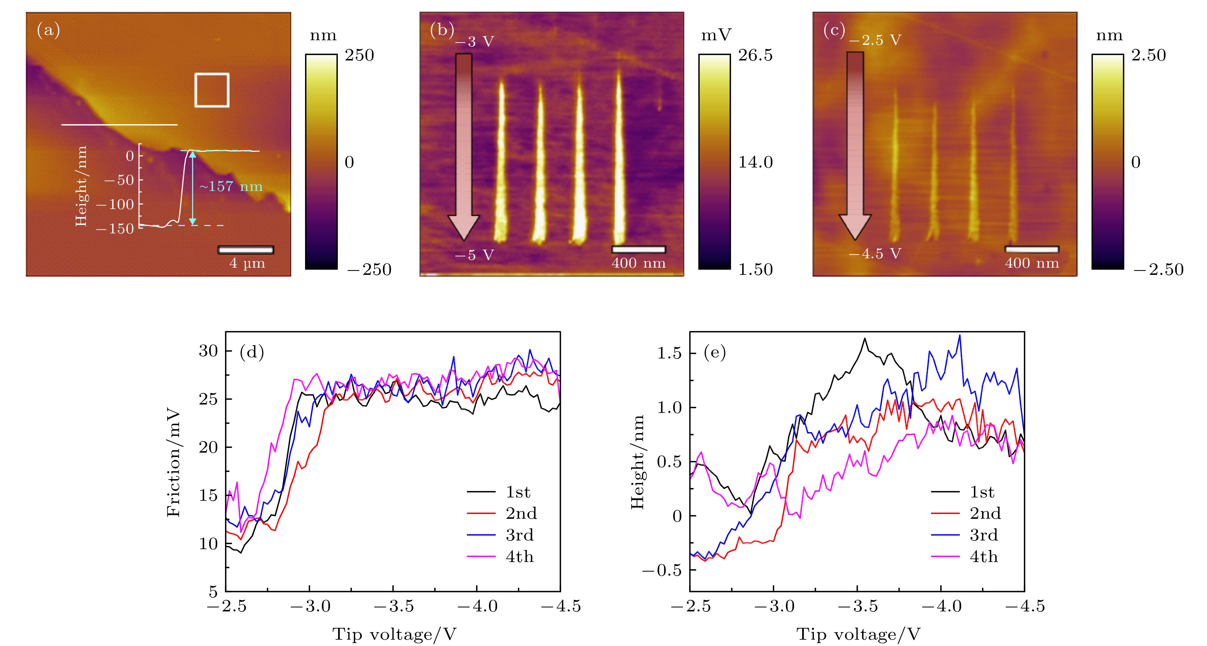
Friction-controlled graphene has great potential as a solid lubricant in micro/nano electromechanical systems. In this work, the conductive atomic force microscope was used to conduct oxidation etching on the graphene surface to produce different nanoscale patterns. The frictional properties of graphene nanoscale patterns were compared under different etching parameters, and the degree of oxidation of the etching patterns was analyzed by Scanning Kelvin Probe Microscopy. The results indicated that the degree of graphene oxidation can be controlled by changing the tip voltage, load and thickness so that graphene forms stable, adjustable oxidation point, line and nanometer patterns on the Au/SiO2/Si substrate. The diameter of oxidation point and width of oxidation line increased with the increase of voltage. The continuity and uniformity of nanometer patterns was improved by Increasing the thickness of graphene. The friction increased with the increase of tip voltage, which was attributed to the increase of meniscus force and electrostatic force. These nanostructures can precisely regulate nano-friction of graphene surface. The realization of the processing of nanoscale patterns and the adjustment of nano-friction characteristics provides a new idea and method for the study of electrical friction behavior of graphene in micro/nano electromechanical systems and the preparation of nano-devices with patterned surfaces.
-
Keywords:
- graphene /
- nano-friction /
- oxidized lithography /
- conductive atomic force microscope
[1] Hainsworth S 2008 Tribology on the Small Scale: A Bottom Up Approach to Friction, Lubrication, and Wear (New York: Oxford University Press) pp3–10
[2] Lee C, Li Q, Kalb W, Liu X Z, Berger H, Carpick R W, Hone J 2010 Science 328 76
 Google Scholar
[3] Klemenz A, Pastewka L, Balakrishna S G, Caron A, Bennewitz R, Moseler M 2014 Nano Lett. 14 7145
 Google Scholar
[4] Lee C, Wei X, Kysar J W, Hone J 2008 Science 321 385
 Google Scholar
[5] Cho DH, Wang L, Kim JS, Lee GH, Kim E S, Lee S, Lee S Y, Hone J, Lee C 2013 Nanoscale 5 3063
 Google Scholar
[6] Zeng X, Peng Y, Lang H 2017 Carbon 118 233
 Google Scholar
[7] Bhowmick S, Banerji A, Alpas A T 2015 Carbon 87 374
 Google Scholar
[8] Zhang Y, Dong M, Gueye B, Ni Z, Wang Y, Chen Y 2015 Appl. Phys. Lett. 107 011601
 Google Scholar
[9] Ko JH, Kwon S, Byun IS, Choi J S, Park B H, Kim Y H, Park J Y 2013 Tribol. Lett. 50 137
 Google Scholar
[10] Fessler G, Eren B, Gysin U, Glatzel T, Meyer E 2014 Appl. Phys. Lett. 104 041910
 Google Scholar
[11] Choi M S, Lee S H, Yoo W J 2011 J. Appl. Phys. 110 073305
 Google Scholar
[12] Masubuchi S, Arai M, Machida T 2011 Nano Lett. 11 4542
 Google Scholar
[13] Kurra N, Reifenberger R G, Kulkarni G U 2014 ACS Appl. Mater. Interfaces 6 6147
 Google Scholar
[14] Masubuchi S, Ono M, Yoshida K, Hirakawa K, Machida T 2009 Appl. Phys. Lett. 94 082107
 Google Scholar
[15] Byun IS, Yoon D, Choi J S, Hwang I, Lee D H, Lee M J, Kawai T, Son YW, Jia Q, Cheong H 2011 ACS Nano 5 6417
 Google Scholar
[16] Colangelo F, Piazza V, Coletti C, Roddaro S, Beltram F, Pingue P 2017 Nanotechnology 28 105709
 Google Scholar
[17] Wagner K, Cheng P, Vezenov D 2011 Langmuir 27 4635
 Google Scholar
[18] Xia Z Y, Pezzini S, Treossi E, Giambastiani G, Corticelli F, Morandi V, Zanelli A, Bellani V, Palermo V 2013 Adv. Funct. Mater. 23 4684
[19] Avdeev V, Monyakina L, Nikol'Skaya I, Sorokina N, Semenenko K 1992 Carbon 30 819
 Google Scholar
[20] Sherpa S D, Levitin G, Hess D W 2012 Appl. Phys. Lett. 101 111602
 Google Scholar
[21] Sherpa S D, Paniagua S A, Levitin G, Marder S R, Williams M, Hess D W 2012 J. Vac. Sci. Technol., B 30 03D
[22] Elinski M B, Menard B D, Liu Z, Batteas J D 2017 J. Phys. Chem. C 121 5635
[23] Butt HJ, Cappella B, Kappl M 2005 Surf. Sci. Rep. 59 1
 Google Scholar
[24] Gómez-Monivas S, Sáenz J J, Calleja M, García R 2003 Phys. Rev. Lett. 91 056101
 Google Scholar
[25] Park J Y, Ogletree D, Thiel P, Salmeron M 2006 Science 313 186
 Google Scholar
-
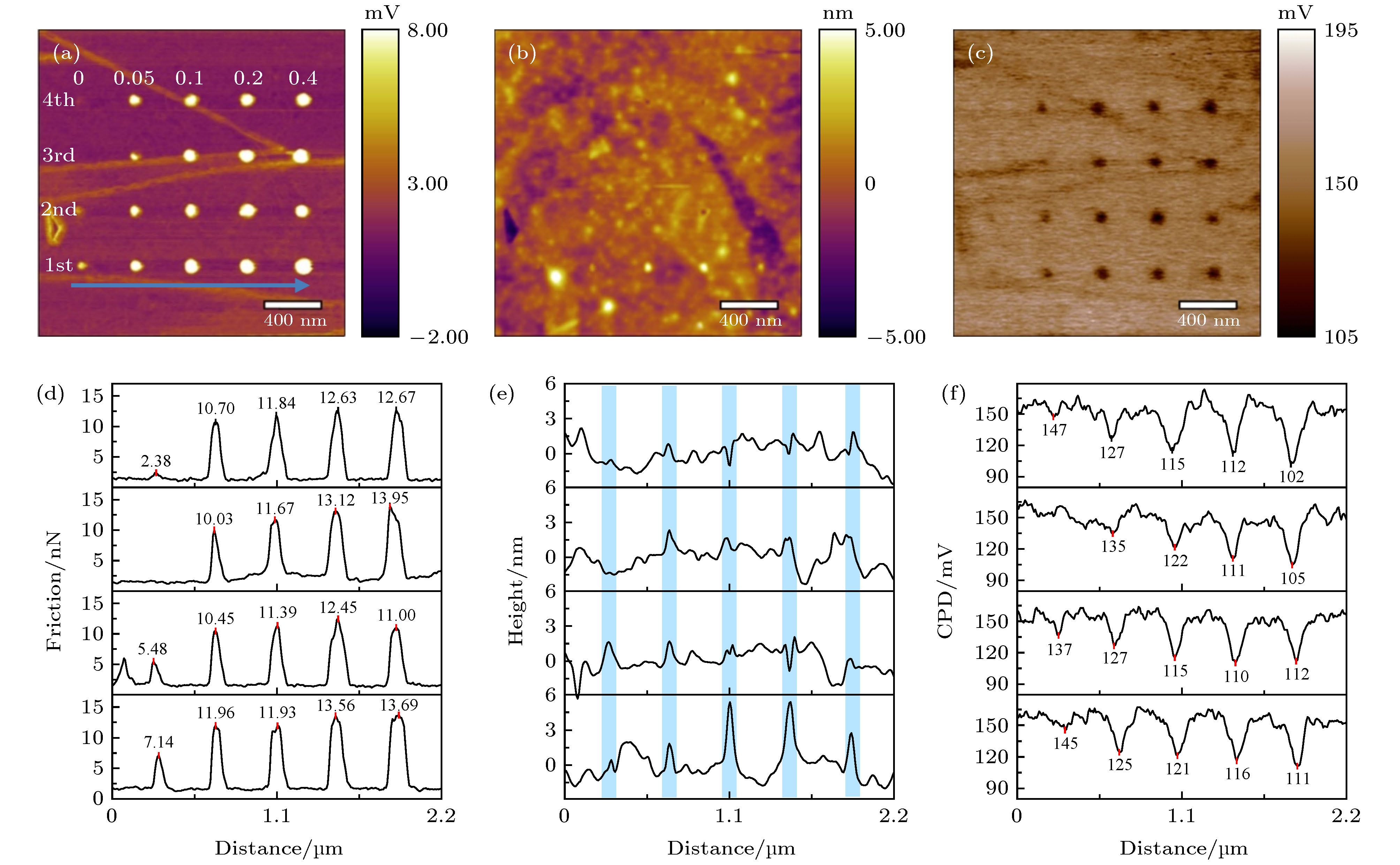
图 3 在相同针尖电压不同接触时间下, 点刻蚀调控石墨烯表面纳米摩擦的结果 (a)摩擦力图; (b)形貌图; (c)接触电势差图像; (d)−(f)分别对应着(a)−(c)中每一行点的摩擦力、高度和接触电势差的变化
Figure 3. Nano-friction of graphene surface was regulated by oxidation points at a constant voltage and different contact time: (a) Friction image; (b) topography image; (c) CPD image; (d)−(f) corresponds to the changes in friction, height and CPD along each row in (a)−(c), respectively.
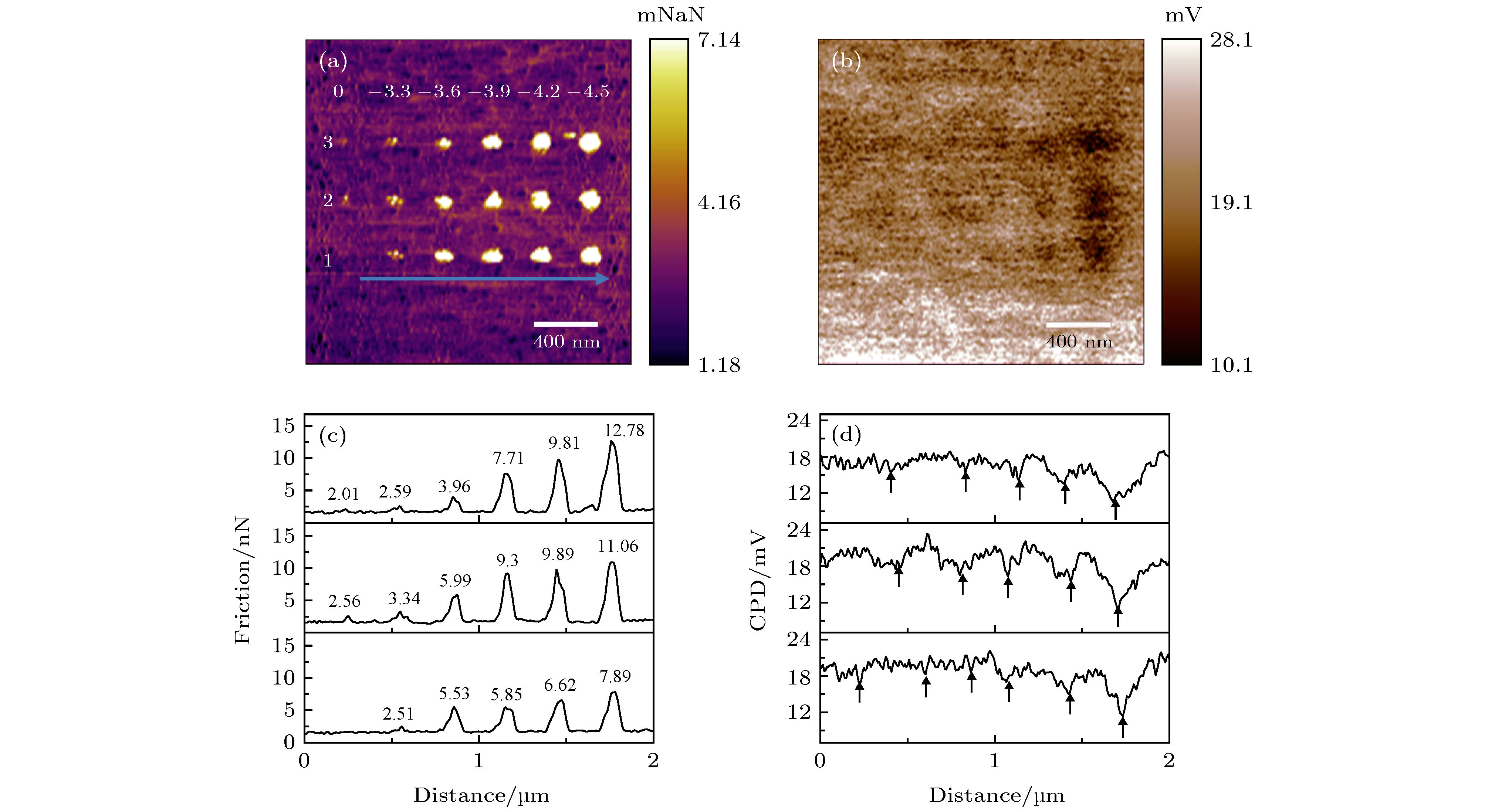
图 4 在相同接触时间不同针尖电压下, 点刻蚀调控石墨烯表面纳米摩擦的结果 (a)摩擦力图; (b)接触电势差图像; (d)和(c)分别对应着(a)和(b)中每一行点的摩擦力和接触电势差的变化
Figure 4. Nano-friction of graphene surface was regulated by oxidation points at a constant contact time and different voltages: (a) Friction image; (b) CPD image; (c) and (d) correspond to the changes in friction and CPD along each row in (a) and (b), respectively.
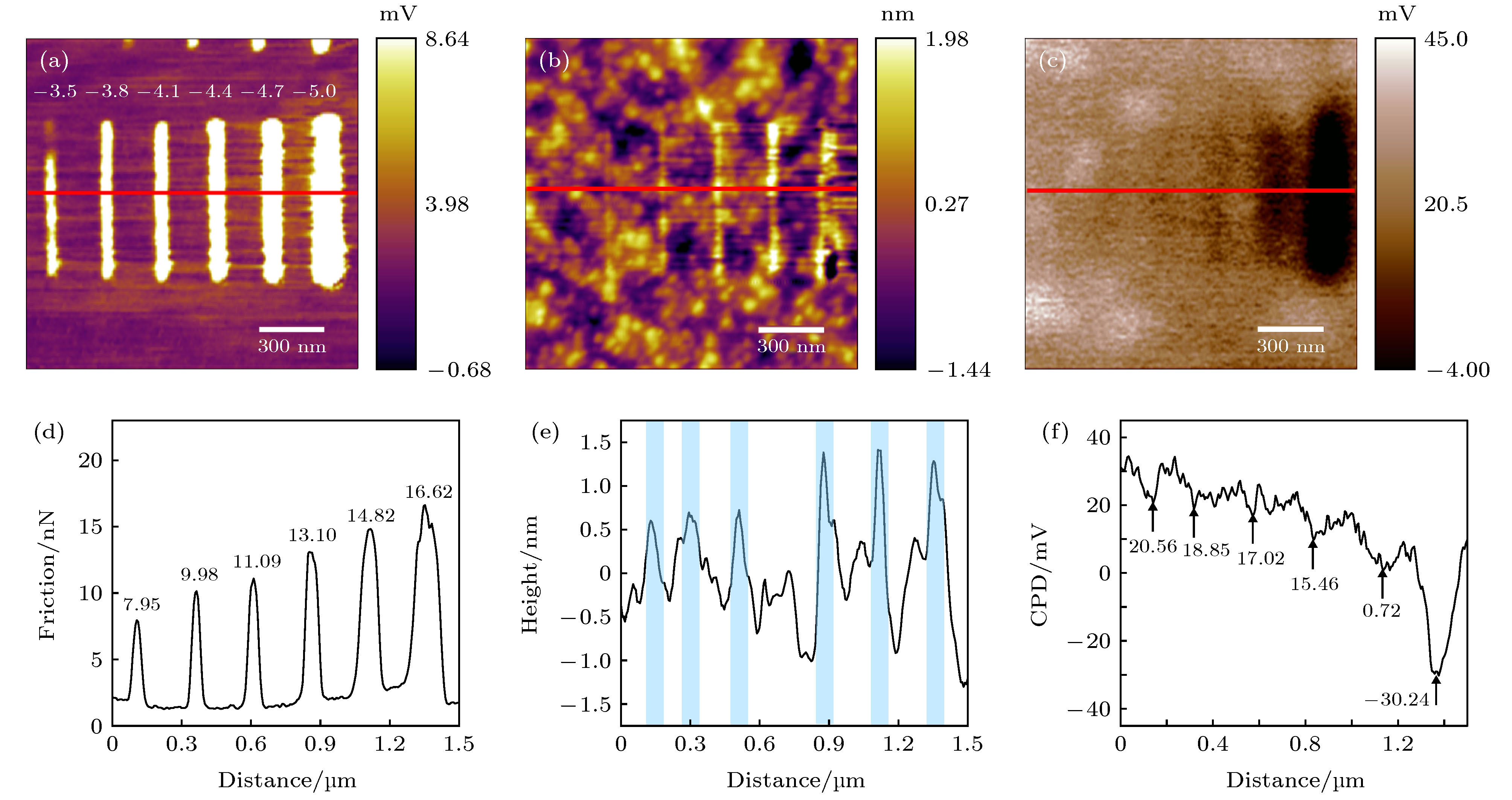
图 5 在相同刻蚀载荷不同针尖电压下, 线刻蚀调控石墨烯纳米摩擦 (a)摩擦力图; (b)形貌图; (c)接触电势差图像; (d)−(f)分别对应着(a)−(c)中红色线的摩擦力、高度和接触电势差的变化
Figure 5. Nano-friction of graphene surface was regulated by oxidation line at a constant load and different voltages: (a) Friction image; (b) topography image; (c) CPD image; (d)−(f) corresponds to the changes in friction, height and CPD along red line in (a)−(c), respectively.
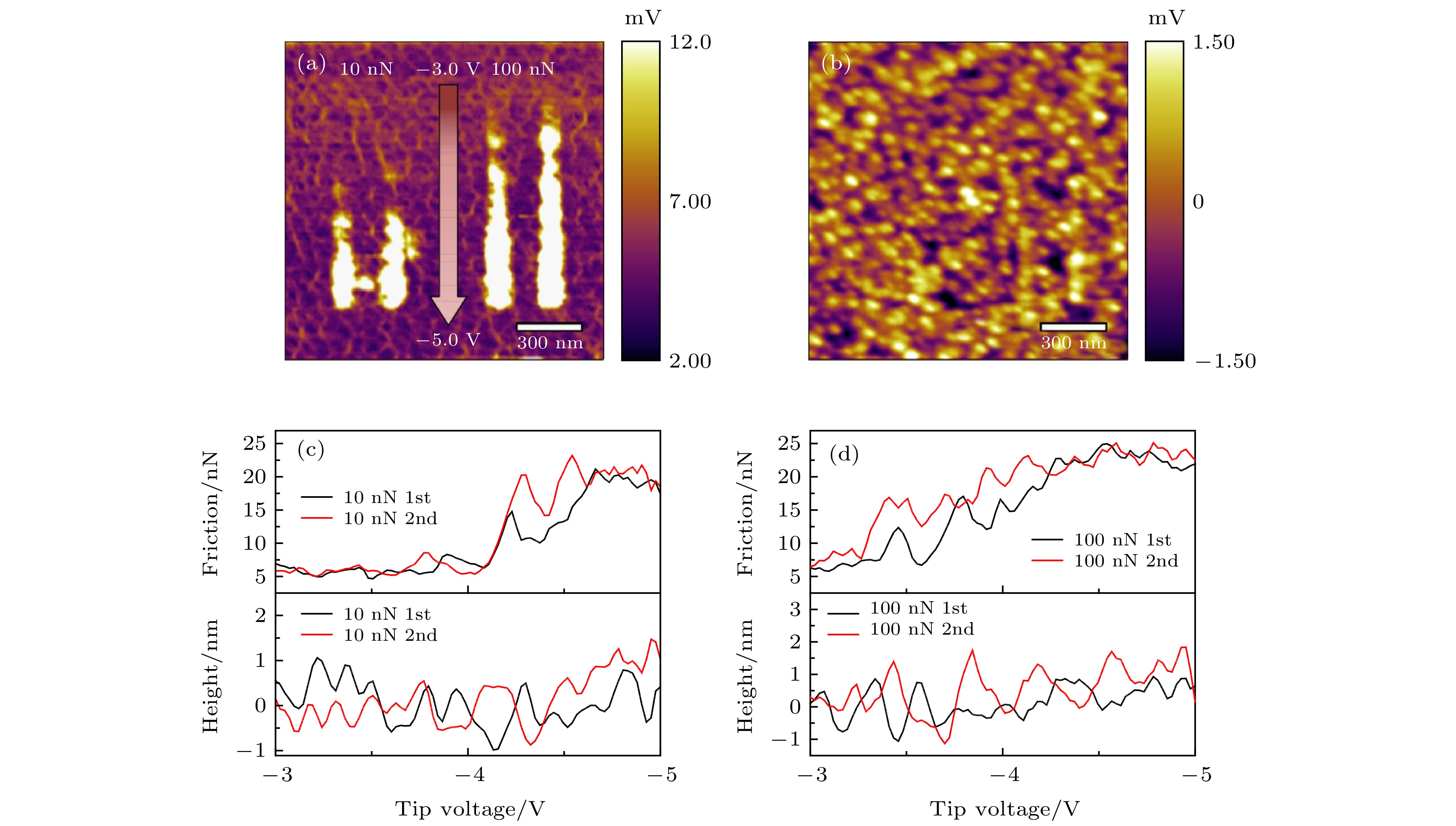
图 6 在相同针尖电压不同刻蚀载荷下, 线刻蚀调控石墨烯纳米摩擦的结果 (a)摩擦力图; (b)形貌图; (c)和(d)分别对应着载荷为10 nN和100 nN时氧化线的摩擦力和高度的变化
Figure 6. Nano-friction of graphene surface was regulated by oxidation line at a constant voltage and different loads: (a) Friction image; (b) topography images; (c) and (d) correspond to the change in friction and height of the oxidation line when the load is 10 nN and 100 nN, respectively.
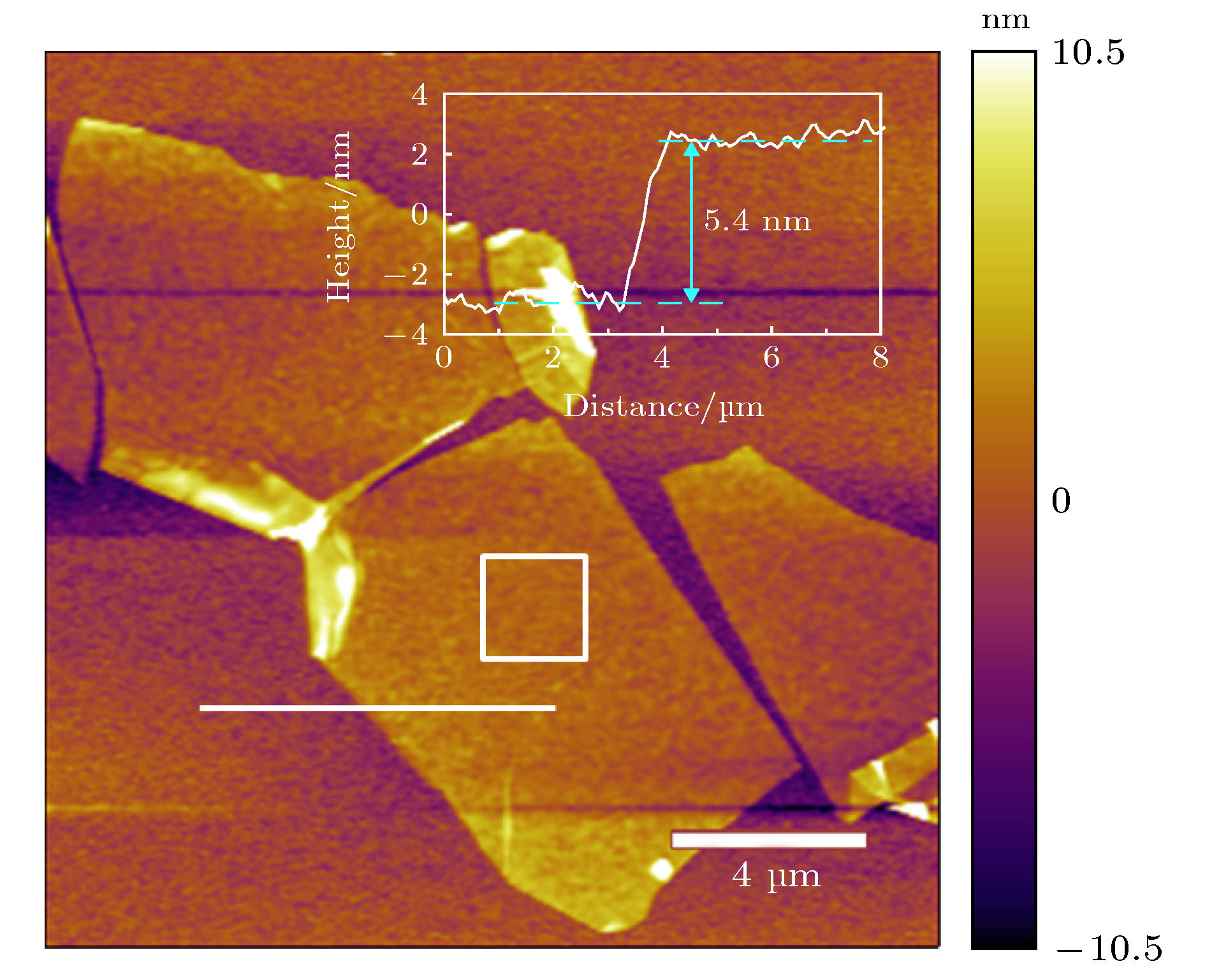
图 7 厚石墨烯上线刻蚀调控石墨烯纳米摩擦 (a)厚石墨烯的AFM形貌图, 插画显示白线的高度轮廓; (b)和(c)分别为(a)中白色方框刻蚀后的摩擦力图和形貌图; (d)和(e)分别为每条刻蚀线的摩擦力和高度变化
Figure 7. Nano-friction of thick graphene surface was regulated by oxidation line: (a) AFM topography image of thick graphene. The inset shows the height profile along white line. (b) and (c) are the friction and topography image of the white box in (a) after etching , respectively; (d) and (e) correspond to the change in friction and height of the oxidation line.
-
[1] Hainsworth S 2008 Tribology on the Small Scale: A Bottom Up Approach to Friction, Lubrication, and Wear (New York: Oxford University Press) pp3–10
[2] Lee C, Li Q, Kalb W, Liu X Z, Berger H, Carpick R W, Hone J 2010 Science 328 76
 Google Scholar
[3] Klemenz A, Pastewka L, Balakrishna S G, Caron A, Bennewitz R, Moseler M 2014 Nano Lett. 14 7145
 Google Scholar
[4] Lee C, Wei X, Kysar J W, Hone J 2008 Science 321 385
 Google Scholar
[5] Cho DH, Wang L, Kim JS, Lee GH, Kim E S, Lee S, Lee S Y, Hone J, Lee C 2013 Nanoscale 5 3063
 Google Scholar
[6] Zeng X, Peng Y, Lang H 2017 Carbon 118 233
 Google Scholar
[7] Bhowmick S, Banerji A, Alpas A T 2015 Carbon 87 374
 Google Scholar
[8] Zhang Y, Dong M, Gueye B, Ni Z, Wang Y, Chen Y 2015 Appl. Phys. Lett. 107 011601
 Google Scholar
[9] Ko JH, Kwon S, Byun IS, Choi J S, Park B H, Kim Y H, Park J Y 2013 Tribol. Lett. 50 137
 Google Scholar
[10] Fessler G, Eren B, Gysin U, Glatzel T, Meyer E 2014 Appl. Phys. Lett. 104 041910
 Google Scholar
[11] Choi M S, Lee S H, Yoo W J 2011 J. Appl. Phys. 110 073305
 Google Scholar
[12] Masubuchi S, Arai M, Machida T 2011 Nano Lett. 11 4542
 Google Scholar
[13] Kurra N, Reifenberger R G, Kulkarni G U 2014 ACS Appl. Mater. Interfaces 6 6147
 Google Scholar
[14] Masubuchi S, Ono M, Yoshida K, Hirakawa K, Machida T 2009 Appl. Phys. Lett. 94 082107
 Google Scholar
[15] Byun IS, Yoon D, Choi J S, Hwang I, Lee D H, Lee M J, Kawai T, Son YW, Jia Q, Cheong H 2011 ACS Nano 5 6417
 Google Scholar
[16] Colangelo F, Piazza V, Coletti C, Roddaro S, Beltram F, Pingue P 2017 Nanotechnology 28 105709
 Google Scholar
[17] Wagner K, Cheng P, Vezenov D 2011 Langmuir 27 4635
 Google Scholar
[18] Xia Z Y, Pezzini S, Treossi E, Giambastiani G, Corticelli F, Morandi V, Zanelli A, Bellani V, Palermo V 2013 Adv. Funct. Mater. 23 4684
[19] Avdeev V, Monyakina L, Nikol'Skaya I, Sorokina N, Semenenko K 1992 Carbon 30 819
 Google Scholar
[20] Sherpa S D, Levitin G, Hess D W 2012 Appl. Phys. Lett. 101 111602
 Google Scholar
[21] Sherpa S D, Paniagua S A, Levitin G, Marder S R, Williams M, Hess D W 2012 J. Vac. Sci. Technol., B 30 03D
[22] Elinski M B, Menard B D, Liu Z, Batteas J D 2017 J. Phys. Chem. C 121 5635
[23] Butt HJ, Cappella B, Kappl M 2005 Surf. Sci. Rep. 59 1
 Google Scholar
[24] Gómez-Monivas S, Sáenz J J, Calleja M, García R 2003 Phys. Rev. Lett. 91 056101
 Google Scholar
[25] Park J Y, Ogletree D, Thiel P, Salmeron M 2006 Science 313 186
 Google Scholar
Catalog
Metrics
- Abstract views: 14021
- PDF Downloads: 203
- Cited By: 0


 DownLoad:

