


-
GaN is known as the third generation of semiconductor and holds promising applications. In this present work, one-dimensional zigzag nanotubes derived from GaN are studied in depth, mainly focusing on their chemical bondings, electronic structures, transport properties, and the regulating effects under gate voltage for nanotubes doped with low-concentration non-metallic atoms in main-groups IIIA-VIIA. Some important findings are obtained, such as the chemical bonds around a heteroatom atom, and their average bond length, binding energy, and chemical formation energy are closely related to the atomic number (the atomic radius), and the charge transfer between heteroatom and nanotubes is directly related to their relative electronegativity. More importantly, we find that although the intrinsic nanotube is a semiconductor, when it is doped with non-metallic atoms, the electronic phase of nanotube possesses an obvious odd-even effect. Namely, after being doped by hetero-atoms in main-groups IIIA, VA, VIIA, nanotubes are semiconductors, but they becomes metals after having been doped with hetero-atoms in main-groups IVA and VIA. This phenomenon has a close relation with the lone-paired electronic state. And also, It is found that with atom doping, the difference between carriers’ mobilities (the hole mobility and electron mobility) of semiconducting tubes can be regulated to reach one order of magnitude, especially the hole mobility and electron mobility can be obviously enhanced by a higher gate voltage. For example, when the gate voltage is increased to 18 V, the hole mobility rises nearly 20 times compared with the case without gate voltage.
-
Keywords:
- GaN nanotube /
- non-metallic atom doping /
- odd-even effect /
- carrier mobility /
- gate voltage effect
[1] Lim D K, Jeon K S, Kim H M, Nam J M, Suh Y D 2010 Nat. Mater. 9 60
 Google Scholar
[2] Novoselov K S, Jiang D, Schedin F, Booth T J, Khotkevich V V, Morozov S V, Geim A K 2005 Proc. Natl. Acad. Sci. 102 10451
Google Scholar
[3] Bolotin K I, Sikes K J, Jiang Z, Klima M, Fudenberg G, Hone J, Kim P, Stormer H L 2008 Solid State Commun. 146 351
Google Scholar
[4] Castro Neto A H, Guinea F, Peres N M R, Novoselov K S, Geim A K 2009 Rev. Mod. Phys. 81 109
Google Scholar
[5] Balandin A A, Ghosh S, Bao W Z, Calizo I, Teweldebrhan D, Miao F, Lau C N 2008 Nano Lett. 8 902
Google Scholar
[6] Tran V, Soklaski R, Liang Y F, Yang L 2014 Phys. Rev. B 89 817
[7] Huang H, Jiang B, Zou X M, Zhao X Z, Liao L 2019 Sci. Bull. 64 1067
Google Scholar
[8] Castellanos-Gomez A, Vicarelli L, Prada E, Island J O, Narasimha-Acharya K L, Blanter S I, Groenendijk D J, Buscema M, Steele G A, Alvarez J V, Zandbergen H W, Palacios J J, van der Zant H S J 2014 2D Mater. 1 025001
[9] Radisavljevic B, Kis A 2013 Nat. Mater. 12 815
Google Scholar
[10] Tareen A K, Khan K, Aslam M, Liu X K, Zhang H 2021 Prog. Solid. State Chem. 61 100294
Google Scholar
[11] Khan K, Tareen A K, Aslam M, Wang R H, Zhang Y P, Mahmood A, Ouyang Z B, Zhang H, Guo Z Y 2020 J. Mater. Chem. C 8 387
Google Scholar
[12] Kobayashi Y, Kumakura K, Akasaka T, Makimoto T 2012 Nature 484 223
Google Scholar
[13] Camacho-Mojica D C, López-Urías F 2015 Sci. Rep. 5 17902
[14] Al Balushi Z Y, Wang Ke, Ghosh R K, Vilá R A, Eichfeld S M, Caldwell J D, Qin X Y, Lin Y C, DeSario P A, Stone G, Subramanian S, Paul D F, Wallace R M, Datta S, Redwing J M, Robinson J A 2016 Nat. Mater. 15 1166
Google Scholar
[15] Chen Y X, Liu K L, Liu J X, Lv T R, Wei B, Zhang T, Zeng M Q, Wang Z C, Fu L 2018 J. Am. Chem. Soc. 140 16392
Google Scholar
[16] Meng X S, Liu H L, Lin L K, Cheng Y B, Hou X, Zhao S Y, Lu H M, Meng X K 2021 Appl. Surf. Sci. 539 148302
Google Scholar
[17] Li S, Xing H Z, Xie R K, ZengY J, Huang Y, Lu A J, Chen X S 2018 Physica E 97 144
Google Scholar
[18] Alaal N, Roqan I S 2020 ACS Omega 5 1261
Google Scholar
[19] Kadioglu Y, Ersan F, Kecik D, Akturk O U, Akturk E, Ciraci S 2018 Phys. Chem. Chem. Phys. 20 16077
Google Scholar
[20] Maier K, Helwig A, Muller G, Hille P, Teubert J, Eickhoff M 2017 Nano Lett. 17 615
Google Scholar
[21] Kong Y K, Liu L, Xia S H, Wang H G, Wang M S 2016 Comput. Theor. Chem. 1092 19
Google Scholar
[22] Goldberger J, He R, Zhang Y F, Lee S, Yan H Q, Choi H J, Yang P D 2003 Nature 34 599
[23] Hemmingsson C, Pozina G, Khromov S, Monemar B 2011 Nanotechnology 22 085602
Google Scholar
[24] Ribeiro C C, de Jesus Gomes Varela J, Guerini S 2018 J. Mol. Model 24 192
Google Scholar
[25] Yang M, Shi J J, Zhang M, Zhang S, Bao Z Q, Luo S J, Zhou T C, Zhu T C, Li X, Li J 2013 Mater. Chem. Phys. 138 225
Google Scholar
[26] Moradian R, Azadi S, Farahani S V 2008 Phys. Lett. A 372 6935
Google Scholar
[27] Kuang W, Hu R, Fan Z Q, Zhang Z H 2019 Nanotechnology 30 145201
Google Scholar
[28] Han J N, Zhang Z H, Fan Z Q, Zhou R L 2020 Nanotechnology 31 315206
Google Scholar
[29] Hu R, Wang D, Fan Z Q, Zhang Z H 2018 Phys. Chem. Chem. Phys. 20 13574
Google Scholar
[30] Fan Z Q, Zhang Z H, Yang S Y 2020 Nanoscale 12 21750
Google Scholar
[31] Zhao T, Fan Z Q, Zhang Z H, Zhou R L 2019 J. Phys. D: Appl. Phys. 52 475301
Google Scholar
[32] Hu R, Li Y H, Zhang Z H, Fan Z Q, Sun L 2019 J. Mater. Chem. C 7 7745
[33] Dong Q X, Hu R, Fan Z Q, Zhang Z H 2018 Carbon 130 206
Google Scholar
[34] Hu J K, Zhang Z H, Fan Z Q, Zhou R L 2019 Nanotechnology 30 485703
Google Scholar
[35] Han J N, He X, Fan Z Q, Zhang Z H 2019 Phys. Chem. Chem. Phys. 21 1830
Google Scholar
[36] Yuan P F, Hu R, Fan Z Q, Zhang Z H 2018 J. Phys.: Condens. Matter 30 445802
Google Scholar
[37] Ma Y D, Dai Y, Guo M, Niu C W, Yu L, Huang B B 2011 Nanoscale 3 2301
Google Scholar
[38] Bardeen J, Shockley W 1950 Phys. Rev. 80 72
Google Scholar
[39] Long M Q, Tang L, Wang D, Wang L J, Shuai Z G 2009 J. Am. Chem. Soc. 131 17728
Google Scholar
[40] Yuan P F, Fan Z Q, Zhang Z H 2017 Carbon 124 228
Google Scholar
-

图 1 (a) GaN纳米带的正视图和侧视图(虚线框内为纳米带单胞); (b) GaN纳米管的正视图和侧视图(虚线框内为纳米管单胞); (c) 本征纳米管的能带结构; (d) 掺杂纳米管的原子结构, X表示掺杂原子, d1, d2, d3分别表示掺杂原子周围的三根共价键
Figure 1. (a) Top and side views of GaN nanoribbon (the black dashed-line box indicates the unit cell of GaN nanoribbon); (b) top and side views of GaN nanotube (the black dashed-line box represents the unit cell of GaN nanotube); (c) band structure of intrinsic nanotube; (d) the atomic structure of doped nanotube, X represents a doped atom, and d1, d2 and d3 are three covalent bonds around a doped atom, respectively.
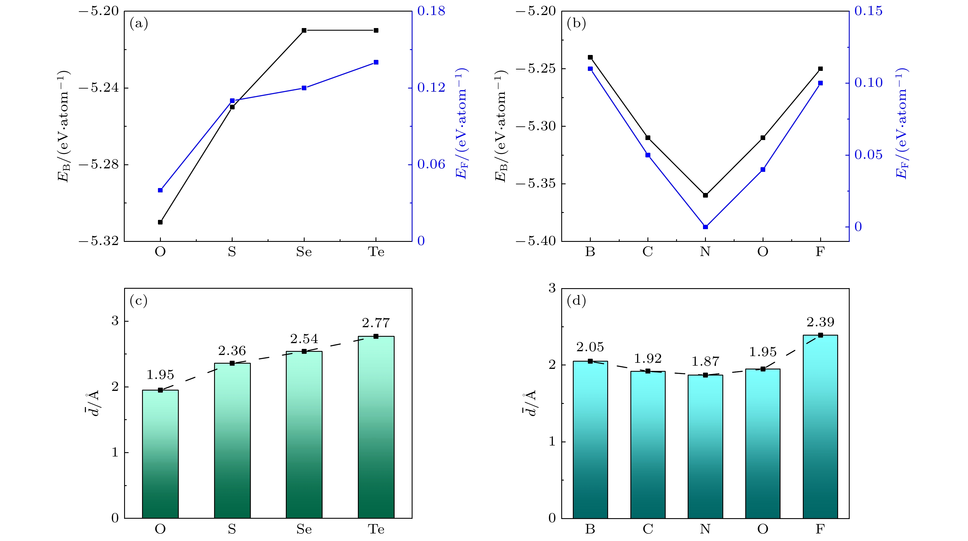
图 2 (a) 纳米管NT-X结合能EB及形成能EF随主族VIA非金属掺杂元素X (= O, S, Se, Te)的变化; (b) 纳米管NT-X结合能EB及形成能EF随第二周期非金属掺杂元素X (= B, C, N, O, F)的变化; (c) NT-X的平均键长
$\bar{d}$ 随主族VIA非金属掺杂元素X (= O, S, Se, Te)的变化; (d) NT-X的平均键长$\bar{d}$ 随第二周期非金属掺杂元素X (= B, C, N, O, F)的变化Figure 2. (a) Formation energy and binding energy versus doped non-metal elements in group VIA for NT-X (X = O, S, Se, Te); (b) formation energy and binding energy versus doped non-metal elements in second period for NT-X (= B, C, N, O, F); (c) averaged bond length
$\bar{d}$ versus doped non-metal elements in group VIA for NT-X (X = O, S, Se, Te); (d) average bond length$\bar{d}$ versus doped non-metal elements in second period for NT-X (= B, C, N, O, F).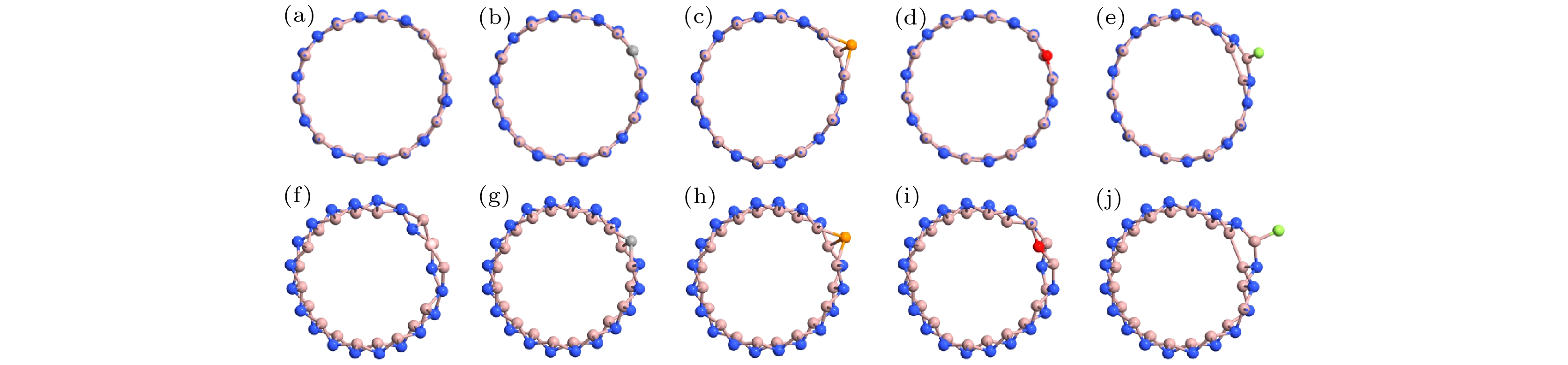
图 3 (a)—(e) B, C, P, O, F掺杂纳米管优化后的几何结构; (f)—(j) B, C, P, O, F掺杂纳米管淬火后的几何结构
Figure 3. (a)–(e) Optimized geometry of B, C, P, O and F doped nanotubes; (f)–(j) geometry of B, C, P, O and F doped nanotubes after annealing simulations.
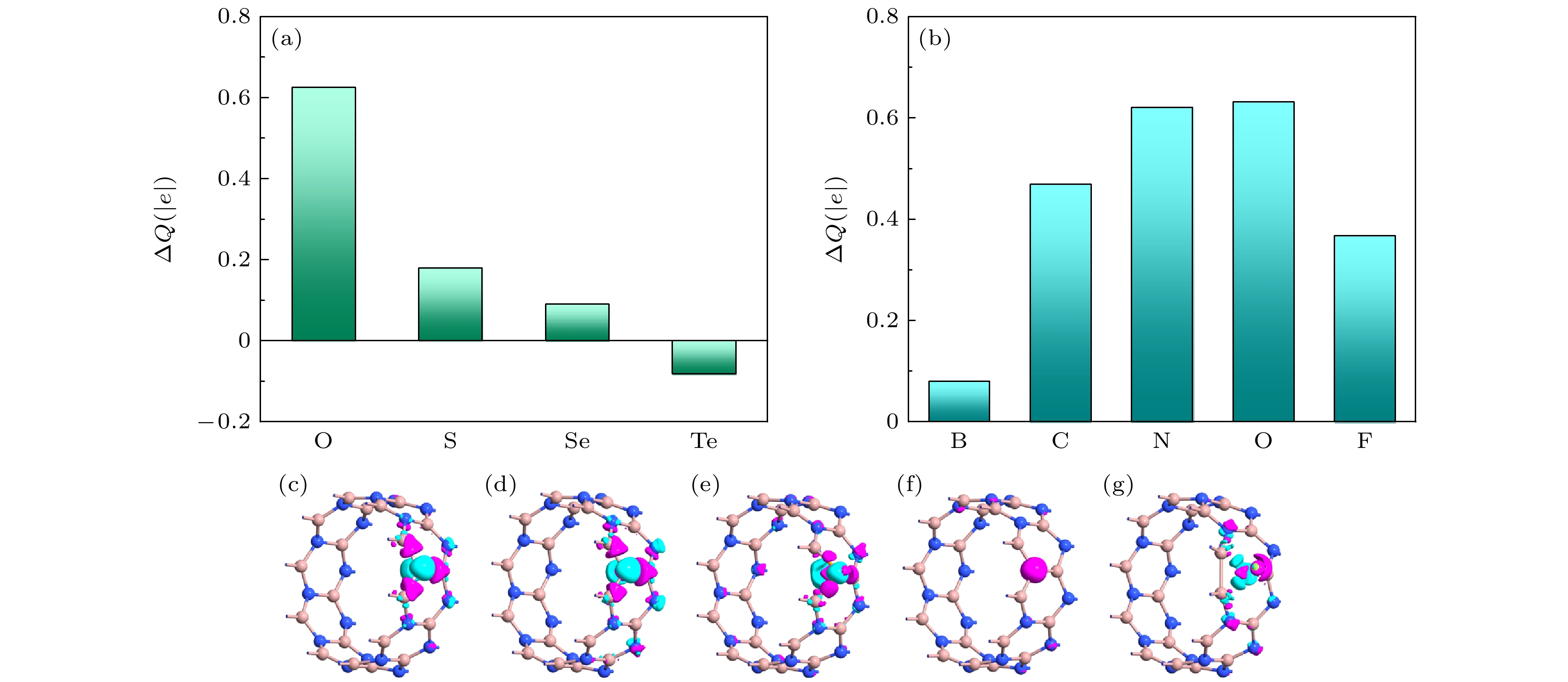
图 4 (a) 主族VIA非金属元素掺杂的纳米管NT-X (X = O, S, Se, Te)的电荷转移; (b) 第二周期非金属元素掺杂的纳米管NT-X (X = B, C, N, O, F)的电荷转移. 掺杂纳米管的电荷差密度 (c) NT-B; (d) NT-C; (e) NT-P; (f) NT-O; (g) NT-F. 青色表示失去电子, 洋红色表示得到电子, 等值面为0.01e/Å3
Figure 4. (a) Charge transfer of group VIA non-metal elements doped NT-X (X = B, C, N, O, F); (b) charge transfer of second period non-metal elements doped NT-X (X = O, S, Se, Te). Charge difference density of doped nanotubes: (c) NT-B; (d) NT-C; (e) NT-P; (f) NT-O; (g) NT-F. Cyan indicates loss of electrons and magenta indicates gain of electrons, and the isosurface is set to 0.01e/Å3.
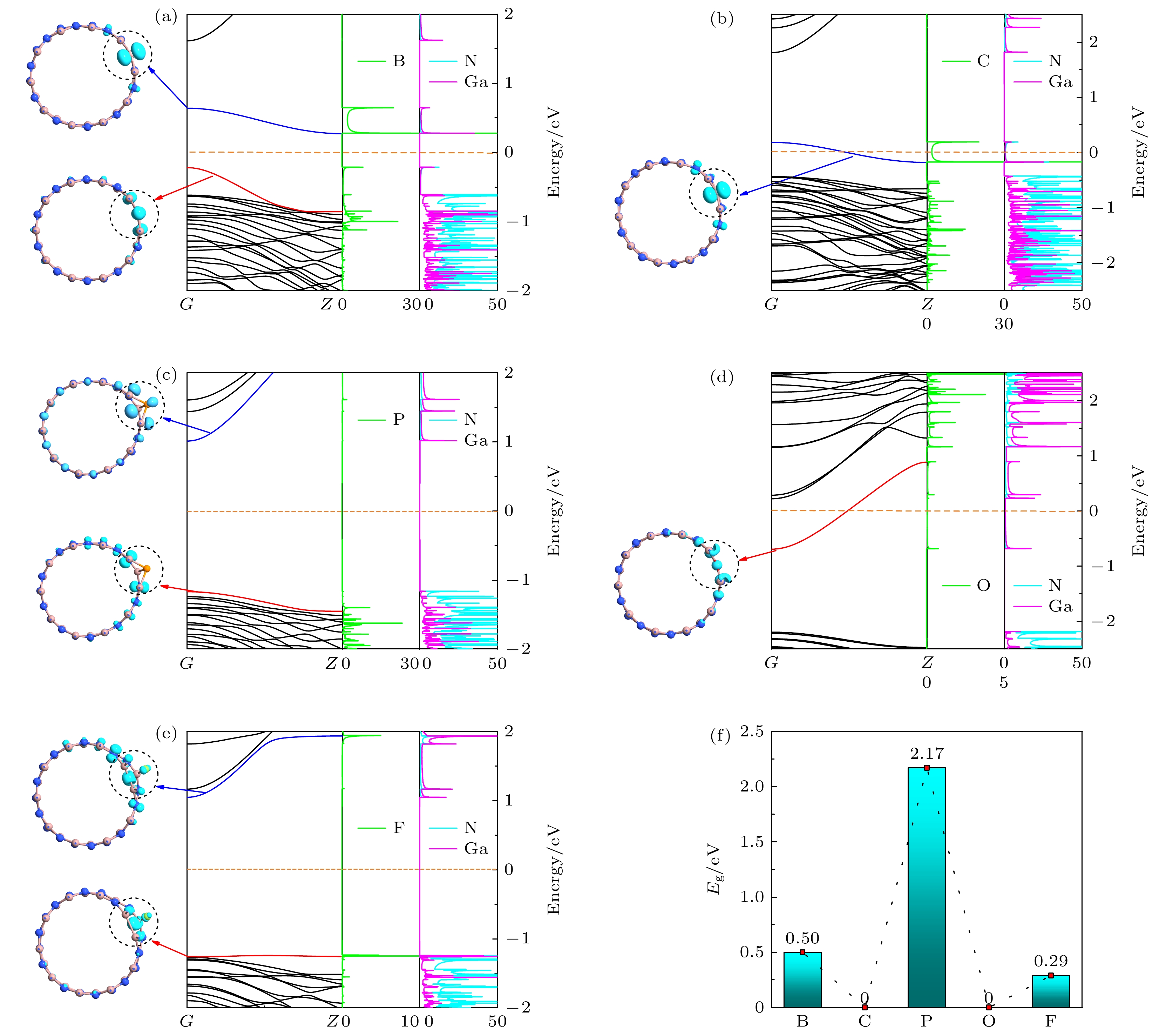
图 5 部分NT-X的能带图以及投影态密度图, 左侧为指定子带的部分电荷密度, 虚线框内为掺杂原子的位置 (a) NT-B; (b) NT-C; (c) NT-P; (d) NT-O; (e) NT-F; (f) NT-X的带隙
Figure 5. The band structure and projected density of states for part of NT-X, the left panel is the partial charge density for designated subbands, and the position of doped atom is shown in the dotted circle: (a) NT-B; (b) NT-C; (c) NT-P; (d) NT-O; (e) NT-F; (f) the band gap for these NT-X.
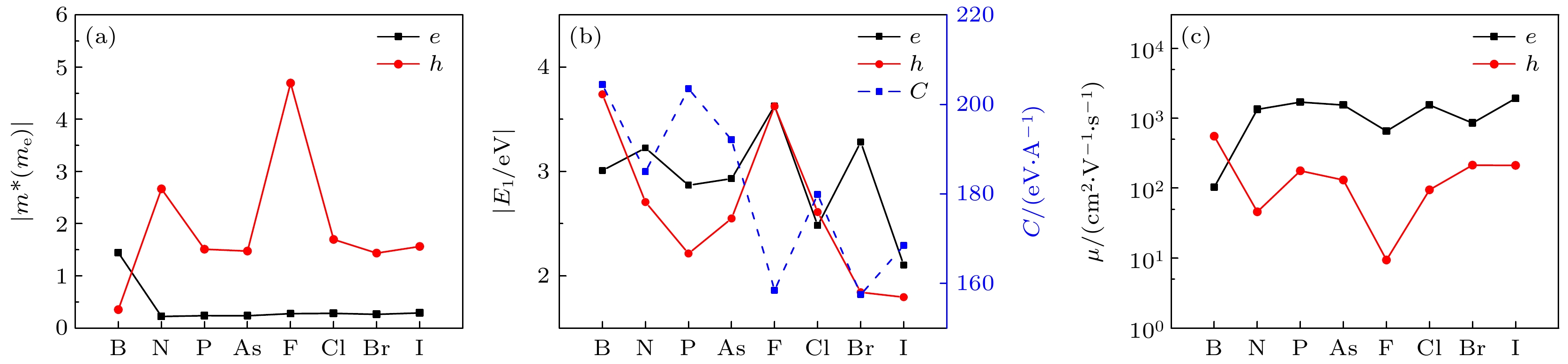
图 6 (a) 半导体性纳米管NT-X (X = B, N, P, As, F, Cl, Br, I)的有效质量m*; (b) NT-X的变形势常数|E1|和拉伸模量C; (c) NT-X的载流子迁移率
Figure 6. (a) Effective mass m* of semiconducting nanotubes NT-X (X = B, N, P, As, F, Cl, Br, I); (b) deformation potential constant | E1 | and tensile modulus C of NT-X; (c) carrier mobility of NT-X.
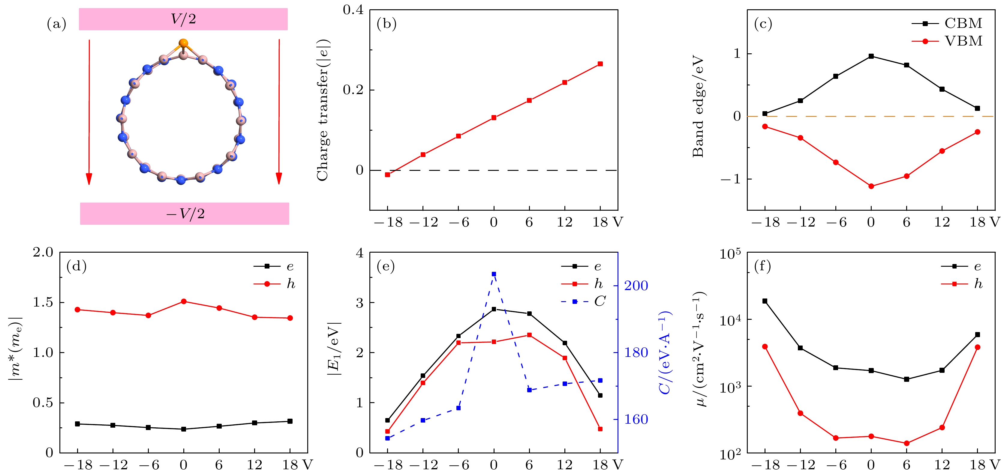
图 7 (a) NT-P外加栅极电压示意图; (b) 不同栅极电压下NT-P中杂质原子P的电荷转移; (c) 不同栅极电压下NT-P的CBM和VBM的变化; (d) NT-P的有效质量m*随栅极电压的变化; (e) NT-P的变形势常数|E1|和拉伸模量C随栅极电压的变化; (f) NT-P的载流子迁移率随栅极电压的变化
Figure 7. (a) The schematic of applied gate voltage on NT-P; (b) electron transfer of hero-atom P in NT-P versus different gate voltages; (c) changes of CBM and VBM under different gate voltages on NT-P; (d) the effective mass m* of NT-P varies with the gate voltage; (e) variation of deformation potential constant |E1| and tensile modulus C of NT-P with gate voltage; (f) the carrier mobility of NT-P varies with the gate voltage.
表 1 掺杂纳米管NT-X的结合能EB及化学形成能EF, 键长di (i = 1, 2, 3)及平均键长
$\bar{d}$ , 电荷转移ΔQ(|e|)(负号表示失去电子), 带隙Eg和电子相EP(金属-M, 半导体-S)Table 1. Binding energy EB, formation energy EF, bond length di (i = 1, 2, 3) and averaged bond length
$\bar{d}$ , charge transfer ΔQ (|e|) (negative sign indicates a loss of electrons), band gap Eg, electronic phase EP (metal-M, semiconductor-S) for the doped nanotubes NT-X.Doped atom EB/(eV· atom–1) EF/(eV· atom–1) d1/Å d2/Å d3/Å $\bar{d}$/Å ΔQ Eg/eV EP IIIA B –5.24 0.11 2.05 2.05 2.04 2.05 +0.08 0.5 S IVA C –5.31 0.05 1.91 1.93 1.93 1.92 +0.469 0 M Si –5.25 0.11 2.41 2.41 2.40 2.41 –0.285 0 M VA N –5.36 0 1.88 1.87 1.87 1.87 +0.621 2.18 S P –5.29 0.07 2.34 2.34 2.30 2.33 +0.148 2.17 S As –5.27 0.08 2.44 2.44 2.39 2.42 –0.186 2.14 S VIA O –5.31 0.04 1.95 1.96 1.94 1.95 +0.636 0 M S –5.25 0.11 2.36 2.37 2.34 2.36 +0.179 0 M Se –5.21 0.12 2.61 2.61 2.39 2.54 +0.091 0 M Te –5.21 0.14 2.86 2.84 2.61 2.77 –0.082 0 M VIIA F –5.25 0.10 2.54 2.76 1.86 2.39 +0.367 2.29 S Cl –5.20 0.14 3.63 2.22 3.33 3.06 +0.265 2.25 S Br –5.20 0.15 3.34 3.38 2.39 3.04 +0.154 2.27 S I –5.19 0.16 3.85 2.57 3.47 3.30 +0.076 2.24 S  DownLoad: CSV
-
[1] Lim D K, Jeon K S, Kim H M, Nam J M, Suh Y D 2010 Nat. Mater. 9 60
Google Scholar
[2] Novoselov K S, Jiang D, Schedin F, Booth T J, Khotkevich V V, Morozov S V, Geim A K 2005 Proc. Natl. Acad. Sci. 102 10451
Google Scholar
[3] Bolotin K I, Sikes K J, Jiang Z, Klima M, Fudenberg G, Hone J, Kim P, Stormer H L 2008 Solid State Commun. 146 351
Google Scholar
[4] Castro Neto A H, Guinea F, Peres N M R, Novoselov K S, Geim A K 2009 Rev. Mod. Phys. 81 109
Google Scholar
[5] Balandin A A, Ghosh S, Bao W Z, Calizo I, Teweldebrhan D, Miao F, Lau C N 2008 Nano Lett. 8 902
Google Scholar
[6] Tran V, Soklaski R, Liang Y F, Yang L 2014 Phys. Rev. B 89 817
[7] Huang H, Jiang B, Zou X M, Zhao X Z, Liao L 2019 Sci. Bull. 64 1067
Google Scholar
[8] Castellanos-Gomez A, Vicarelli L, Prada E, Island J O, Narasimha-Acharya K L, Blanter S I, Groenendijk D J, Buscema M, Steele G A, Alvarez J V, Zandbergen H W, Palacios J J, van der Zant H S J 2014 2D Mater. 1 025001
[9] Radisavljevic B, Kis A 2013 Nat. Mater. 12 815
Google Scholar
[10] Tareen A K, Khan K, Aslam M, Liu X K, Zhang H 2021 Prog. Solid. State Chem. 61 100294
Google Scholar
[11] Khan K, Tareen A K, Aslam M, Wang R H, Zhang Y P, Mahmood A, Ouyang Z B, Zhang H, Guo Z Y 2020 J. Mater. Chem. C 8 387
Google Scholar
[12] Kobayashi Y, Kumakura K, Akasaka T, Makimoto T 2012 Nature 484 223
Google Scholar
[13] Camacho-Mojica D C, López-Urías F 2015 Sci. Rep. 5 17902
[14] Al Balushi Z Y, Wang Ke, Ghosh R K, Vilá R A, Eichfeld S M, Caldwell J D, Qin X Y, Lin Y C, DeSario P A, Stone G, Subramanian S, Paul D F, Wallace R M, Datta S, Redwing J M, Robinson J A 2016 Nat. Mater. 15 1166
Google Scholar
[15] Chen Y X, Liu K L, Liu J X, Lv T R, Wei B, Zhang T, Zeng M Q, Wang Z C, Fu L 2018 J. Am. Chem. Soc. 140 16392
Google Scholar
[16] Meng X S, Liu H L, Lin L K, Cheng Y B, Hou X, Zhao S Y, Lu H M, Meng X K 2021 Appl. Surf. Sci. 539 148302
Google Scholar
[17] Li S, Xing H Z, Xie R K, ZengY J, Huang Y, Lu A J, Chen X S 2018 Physica E 97 144
Google Scholar
[18] Alaal N, Roqan I S 2020 ACS Omega 5 1261
Google Scholar
[19] Kadioglu Y, Ersan F, Kecik D, Akturk O U, Akturk E, Ciraci S 2018 Phys. Chem. Chem. Phys. 20 16077
Google Scholar
[20] Maier K, Helwig A, Muller G, Hille P, Teubert J, Eickhoff M 2017 Nano Lett. 17 615
Google Scholar
[21] Kong Y K, Liu L, Xia S H, Wang H G, Wang M S 2016 Comput. Theor. Chem. 1092 19
Google Scholar
[22] Goldberger J, He R, Zhang Y F, Lee S, Yan H Q, Choi H J, Yang P D 2003 Nature 34 599
[23] Hemmingsson C, Pozina G, Khromov S, Monemar B 2011 Nanotechnology 22 085602
Google Scholar
[24] Ribeiro C C, de Jesus Gomes Varela J, Guerini S 2018 J. Mol. Model 24 192
Google Scholar
[25] Yang M, Shi J J, Zhang M, Zhang S, Bao Z Q, Luo S J, Zhou T C, Zhu T C, Li X, Li J 2013 Mater. Chem. Phys. 138 225
Google Scholar
[26] Moradian R, Azadi S, Farahani S V 2008 Phys. Lett. A 372 6935
Google Scholar
[27] Kuang W, Hu R, Fan Z Q, Zhang Z H 2019 Nanotechnology 30 145201
Google Scholar
[28] Han J N, Zhang Z H, Fan Z Q, Zhou R L 2020 Nanotechnology 31 315206
Google Scholar
[29] Hu R, Wang D, Fan Z Q, Zhang Z H 2018 Phys. Chem. Chem. Phys. 20 13574
Google Scholar
[30] Fan Z Q, Zhang Z H, Yang S Y 2020 Nanoscale 12 21750
Google Scholar
[31] Zhao T, Fan Z Q, Zhang Z H, Zhou R L 2019 J. Phys. D: Appl. Phys. 52 475301
Google Scholar
[32] Hu R, Li Y H, Zhang Z H, Fan Z Q, Sun L 2019 J. Mater. Chem. C 7 7745
[33] Dong Q X, Hu R, Fan Z Q, Zhang Z H 2018 Carbon 130 206
Google Scholar
[34] Hu J K, Zhang Z H, Fan Z Q, Zhou R L 2019 Nanotechnology 30 485703
Google Scholar
[35] Han J N, He X, Fan Z Q, Zhang Z H 2019 Phys. Chem. Chem. Phys. 21 1830
Google Scholar
[36] Yuan P F, Hu R, Fan Z Q, Zhang Z H 2018 J. Phys.: Condens. Matter 30 445802
Google Scholar
[37] Ma Y D, Dai Y, Guo M, Niu C W, Yu L, Huang B B 2011 Nanoscale 3 2301
Google Scholar
[38] Bardeen J, Shockley W 1950 Phys. Rev. 80 72
Google Scholar
[39] Long M Q, Tang L, Wang D, Wang L J, Shuai Z G 2009 J. Am. Chem. Soc. 131 17728
Google Scholar
[40] Yuan P F, Fan Z Q, Zhang Z H 2017 Carbon 124 228
Google Scholar

 DownLoad:


Catalog
Metrics
- Abstract views: 8275
- PDF Downloads: 133
- Cited By: 0
