


-
As one of the most important semiconductor materials, silicon (Si) is widely used in optoelectronic devices such as solar cells and photodetectors. Owing to the difference in refractive index between silicon and air, a large amount of incident light is reflected back into the air from the silicon surface. In order to suppress the loss caused by this reflection, a variety of silicon nanostructures with strong trapping effect have been developed. Most of the dry-etching schemes encounter the problems of high cost and complex preparation, while the silicon nanowires array prepared by the wet-etching schemes has the problems of low controllability of some parameters such as the spacing between two adjacent nanowires, and the small effective area of heterojunction. The method of using polystyrene microsphere as the mask can integrate the advantages of dry-etching method and wet-etching method, and it is easy to obtain periodic silicon nanowires (pillars) array. In this paper, first, we summarize the properties and preparation methods for silicon nanowires structure, the strategies to effectively improve the performance of silicon nanowires (pillars) array photodetectors, Then we analyze the existing problems. Further, the latest developments of silicon nanowires (pillars) array photodetector are discussed, and the structure, morphology of photosensitive layer and methods to improve the performance parameters of silicon nanowires (pillars) array photodetector are analyzed. Among them, we focus on the ultraviolet light sensitive silicon based photodetector and its method to show tunable and selective resonance absorption through leaky mode resonance, the silicon nanowires array photodetector modified with metal nanoparticles and the method of improving performance through surface plasmon effect, and plasmon hot electrons. Heterojunction photodetectors composed of various low-dimensional materials and silicon nanowires (pillars) array, and methods to improve the collection efficiency of photogenerated charge carriers through the “core/shell” structure, methods to expand the detection band range of silicon-based photodetectors by integrating down-conversion light-emitting materials and silicon nanowires (pillars) array, flexible silicon nanowires array photodetectors and their various preparation methods, are all introduced. Then, the main problems that a large number of defect states will be generated on the silicon nanostructure surface in the MACE process are briefly introduced, and several possible solutions for defect passivation are also presented. Finally, the future development for silicon nanowires (pillars) array photodetectors is prospected.
-
Keywords:
- silicon nanowires /
- silicon nanowires array /
- dry-etching and wet-etching /
- metal-assisted chemical etching /
- photodetectors
[1] Li C, Liu D, Dai D 2019 Nanophotonics 8 227
 Google Scholar
[2] Adinolfi V, Sargent E H 2017 Nature 542 324
Google Scholar
[3] Lee S H, Kang J S, Kim D 2018 Materials 11 2557
Google Scholar
[4] Margalit N, Xiang C, Bowers S M, Bjorlin A, Blum R, Bowers J E 2021 Appl. Phys. Lett. 118 220501
Google Scholar
[5] Wang Y, Ding K, Sun B, Lee ST, Jie J 2016 Nano Res. 9 72
Google Scholar
[6] Liu C, Guo J, Yu L, Li J, Zhang M, Li H, Shi Y, Dai D 2021 Light Sci. Appl. 10 123
Google Scholar
[7] Zhou J, Xin K, Zhao X, Li D, Wei Z, Xia J 2022 Sci. China Mater. 65 876
Google Scholar
[8] Liu J J, Qu J L, Kirchartz T, Song J 2021 J. Mater. Chem. A 9 20919
Google Scholar
[9] Li C, Zhao J H, Chen Z G 2021 J. Alloy. Compd. 883 160765
Google Scholar
[10] Arjmand T, Legallais M, Nguyen T T T, et al. 2022 Nanomaterials 12 1043
Google Scholar
[11] Donnelly V M, Kornblit A 2013 J. Vac. Sci. Technol. 31 050825
Google Scholar
[12] Huo C, Wang J, Fu H, Li X, Yang Y, Wang H, Mateen A, Farid G, Peng K Q 2020 Adv. Funct. Mater. 30 2005744
Google Scholar
[13] Tian W, Sun H, Chen L, Wangyang P, Chen X, Xiong J, Li L 2019 InfoMat 1 140
Google Scholar
[14] Um H D, Solanki A, Jayaraman A, Gordon R G, Habbal F 2019 ACS Nano 13 11717
Google Scholar
[15] Wang X, Tang Y, Wang W, Zhao H, Song Y, Kang C, Wang K 2022 Nanomaterials 12 1824
Google Scholar
[16] Rasool K, Rafiq M A, Ahmad M, Imran Z, Batool S S, Hasan M M 2013 AIP Adv. 3 082111
Google Scholar
[17] Liu J Y, Wang J J, Lin D H, Wang J, Fu C, Liang F X, Li X, Gu Z P, Wu D, Luo L B 2022 ACS Appl. Mater. Interfaces 14 32341
Google Scholar
[18] Ohmi T, Imaoka T, Kezuka T, Takano J, Kogure M 1993 J. Electrochem. Soc. 140 811
Google Scholar
[19] Morinaga H, Suyama M, Ohmi T 1994 J. Electrochem. Soc. 141 2834
Google Scholar
[20] Kim J S, Morita H, Joo J D, Ohmi T 1997 J. Electrochem. Soc. 144 3275
Google Scholar
[21] Morinaga H, Futatsuki T, Ohmi T, Fuchita E, Oda M, Hayashi C 1995 J. Electrochem. Soc. 142 966
Google Scholar
[22] Peng K, Wu Y, Fang H, Zhong X, Xu Y, Zhu J 2005 Angew. Chem. Int. Edit. 44 2737
Google Scholar
[23] Peng K Q, Hu J J, Yan Y J, Wu Y, Fang H, Xu Y, Lee S T, Zhu J 2006 Adv. Funct. Mater. 16 387
Google Scholar
[24] Peng K, Lu A, Zhang R, Lee S T 2008 Adv. Funct. Mater. 18 3026
Google Scholar
[25] Zhang X G, Collins S D, Smith R L 1989 J. Electrochem. Soc. 136 1561
Google Scholar
[26] Kolasinski K W 2010 J. Phys. Chem. C 114 22098
Google Scholar
[27] Turner D R 1960 J. Electrochem. Soc. 107 810
Google Scholar
[28] Peng K Q, Yan Y J, Gao S P, Zhu J 2002 Adv. Mater. 14 1164
Google Scholar
[29] Koynov S, Brandt M S, Stutzmann M 2006 Appl. Phys. Lett. 88 203107
Google Scholar
[30] Peng K, Fang H, Hu J, Wu Y, Zhu J, Yan Y, Lee S 2006 Chem. Eur. J. 12 7942
Google Scholar
[31] Peng K, Zhu J 2003 J. Electroanal. Chem. 558 35
Google Scholar
[32] Tsujino K, Matsumura M 2005 Electrochem. Solid-St. 8 C193
Google Scholar
[33] Hildreth O J, Fedorov A G, Wong C P 2012 ACS Nano 6 10004
Google Scholar
[34] Chen H, Wang H, Zhang X H, Lee C S, Lee S T 2010 Nano Lett. 10 864
Google Scholar
[35] Kim J, Kim Y H, Choi S H, Lee W 2011 ACS Nano 5 5242
Google Scholar
[36] Chen Y, Li L, Zhang C, Tuan C C, Chen X, Gao J, Wong C P 2017 Nano Lett. 17 1014
Google Scholar
[37] Chen Y, Zhang C, Li L, Tuan C C, Wu F, Chen X, Gao J, Ding Y, Wong C P 2017 Nano Lett. 17 4304
Google Scholar
[38] Huang Z, Fang H, Zhu J 2007 Adv. Mater. 19 744
Google Scholar
[39] Pudasaini P R, Ruiz-Zepeda F, Sharma M, Elam D, Ponce A, Ayon A A 2013 ACS Appl. Mater. Interfaces 5 9620
Google Scholar
[40] Hochbaum A I, Chen R, Delgado R D, Liang W, Garnett E C, Najarian M, Majumdar A, Yang P 2008 Nature 451 163
Google Scholar
[41] Hildreth O J, Brown D, Wong C P 2011 Adv. Funct. Mater. 21 3119
Google Scholar
[42] Wang J, Hu Y, Zhao H, Fu H, Wang Y, Huo C, Peng K Q 2018 Adv. Mater. Interfaces 5 1801132
Google Scholar
[43] Lai R A, Hymel T M, Narasimhan V K, Cui Y 2016 ACS Appl. Mater. Interfaces 8 8875
Google Scholar
[44] Li L, Tuan C C, Zhang C, Chen Y, Lian G, Wong C P 2019 J. Microelectromech. Syst. 28 143
Google Scholar
[45] Li L, Zhao X, Wong C P 2015 ECS J. Solid State Sci. Technol. 4 P337
Google Scholar
[46] Li Y, Shi Z F, Li X J, Shan C X 2019 Chin. Phys. B 28 017803
Google Scholar
[47] Han C, Chen Z, Zhang N, Colmenares J C, Xu Y J 2015 Adv. Funct. Mater. 25 221
Google Scholar
[48] Reddy A L M, Gowda S R, Shaijumon M M, Ajayan P M 2012 Adv. Mater. 24 5045
Google Scholar
[49] Lu W, Lieber C M 2007 Nat. Mater. 6 841
Google Scholar
[50] Li Y, Wang H, Xie L, Liang Y, Hong G, Dai H 2011 J. Am. Chem. Soc. 133 7296
Google Scholar
[51] Kholmanov I N, Domingues S H, Chou H, et al. 2013 ACS Nano 7 1811
Google Scholar
[52] Huang Z G, Lin X X, Zeng Y, et al. 2015 Sol. Energy Mater. Sol. Cells 143 302
Google Scholar
[53] Sivakov V, Andrä G, Gawlik A, Berger A, Plentz J, Falk F, Christiansen S H 2009 Nano Lett. 9 1549
Google Scholar
[54] Wan X, Xu Y, Guo H, et al. 2017 NPJ 2D Mater. Appl. 1 4
Google Scholar
[55] Mokkapati S, Saxena D, Tan H H, Jagadish C 2015 Sci. Rep. 5 15339
Google Scholar
[56] Fountaine K T, Whitney W S, Atwater H A 2014 J. Appl. Phys. 116 153106
Google Scholar
[57] Cao L, White J S, Park J S, Schuller J A, Clemens B M, Brongersma M L 2009 Nat. Mater. 8 643
Google Scholar
[58] Wang B, Leu P W 2012 Opt. Lett. 37 3756
Google Scholar
[59] Wang J J, Fu C, Cheng H Y, Tong X W, Zhang Z X, Wu D, Chen L M, Liang F X, Luo L B 2021 ACS Nano 15 16729
Google Scholar
[60] Nusir A I, Bauman S J, Marie M S, Herzog J B, Manasreh M O 2017 Appl. Phys. Lett. 111 171103
Google Scholar
[61] Luo L B, Zeng L H, Xie C, Yu Y Q, Liang F X, Wu C Y, Wang L, Hu J G 2014 Sci. Rep. 4 3914
Google Scholar
[62] Kim K, Yoon S, Seo M, Lee S, Cho H, Meyyappan M, Baek C K 2019 Nat. Electron. 2 572
Google Scholar
[63] Vasa P, Lienau C 2010 Angew. Chem. Int. Edit. 49 2476
Google Scholar
[64] Schaadt D M, Feng B, Yu E T 2005 Appl. Phys. Lett. 86 063106
Google Scholar
[65] Qi Z, Zhai Y, Wen L, Wang Q, Chen Q, Iqbal S, Chen G, Xu J, Tu Y 2017 Nanotechnology 28 275202
Google Scholar
[66] Huang Y, Liang H, Zhang Y, Yin S, Cai C, Liu W, Jia T 2021 ACS Appl. Nano Mater. 4 1567
Google Scholar
[67] Wang H, Wang F, Xu T, et al. 2021 Nano Lett. 21 7761
Google Scholar
[68] Mao C H, Dubey A, Lee F J, et al. 2021 ACS Appl. Mater. Interfaces 13 4126
Google Scholar
[69] Xie C, Nie B, Zeng L, Liang F X, Wang M Z, Luo L, Feng M, Yu Y, Wu C Y, Wu Y, Yu S H 2014 ACS Nano 8 4015
Google Scholar
[70] Mondal H, Dey T, Basori R 2021 ACS Appl. Nano Mater. 4 11938
Google Scholar
[71] Chandra A, Giri S, Das B, Ghosh S, Sarkar S, Chattopadhyay K K 2021 Appl. Surf. Sci. 548 149256
Google Scholar
[72] Liang W, Wang L, Li Y, Zhang F, Chen X, Wu D, Tian Y, Li X, Shan C, Shi Z 2021 Mater. Today Phys. 18 100398
Google Scholar
[73] Feng B, Pan X, Liu T, Tian S, Wang T, Chen Y 2021 Nano Lett. 21 5655
Google Scholar
[74] Tong X W, Wang J J, Li J X, Hu X F, Wu D, Luo L B 2021 Sensor. Actuat. A-Phys. 322 112625
Google Scholar
[75] Sun K, Jing Y, Park N, Li C, Bando Y, Wang D 2010 J. Am. Chem. Soc. 132 15465
Google Scholar
[76] Hong Q, Cao Y, Xu J, Lu H, He J, Sun J L 2014 ACS Appl. Mater. Interfaces 6 20887
Google Scholar
[77] Cao Y, Zhu J, Xu J, He J, Sun J L, Wang Y, Zhao Z 2014 Small 10 2345
Google Scholar
[78] Das B, Das N S, Sarkar S, Chatterjee B K, Chattopadhyay K K 2017 ACS Appl. Mater. Interfaces 9 22788
Google Scholar
[79] Gong C, Zhang Y, Chen W, Chu J, Lei T, Pu J, Dai L, Wu C, Cheng Y, Zhai T, Li L, Xiong J 2017 Adv. Sci. 4 1700231
Google Scholar
[80] Henning A, Sangwan V K, Bergeron H, et al. 2018 ACS Appl. Mater. Interfaces 10 16760
Google Scholar
[81] Asuo I M, Banerjee D, Pignolet A, Nechache R, Cloutier S G 2021 Phys. Status Solidi R. 15 2000537
Google Scholar
[82] Zhao J, Liu H, Deng L, Bai M, Xie F, Wen S, Liu W 2021 Sensors 21 6146
Google Scholar
[83] Mao J, Zhang B, Shi Y, Wu X, He Y, Wu D, Jie J, Lee C S, Zhang X 2022 Adv. Funct. Mater. 32 2108174
Google Scholar
[84] Lu J, Sheng X, Tong G, Yu Z, Sun X, Yu L, Xu X, Wang J, Xu J, Shi Y, Chen K 2017 Adv. Mater. 29 1700400
Google Scholar
[85] Mihalache I, Radoi A, Pascu R, Romanitan C, Vasile E, Kusko M 2017 ACS Appl. Mater. Interfaces 9 29234
Google Scholar
[86] Zhang M, Wang L, Meng L, et al. 2018 Adv. Opt. Mater. 6 1800077
Google Scholar
[87] Weisse J M, Kim D R, Lee C H, Zheng X 2011 Nano Lett. 11 1300
Google Scholar
[88] Mulazimoglu E, Coskun S, Gunoven M, Butun B, Ozbay E, Turan R, Unalan H E 2013 Appl. Phys. Lett. 103 083114
Google Scholar
[89] Xu Y, Shen H, Yue Z, Wang S, Zhao Q, Wang Z 2022 Surf. Interfaces 33 102288
Google Scholar
[90] Chee K W A, Ghosh B K, Saad I, Hong Y, Xia Q H, Gao P, Ye J, Ding Z J 2022 Nano Energy 95 106899
Google Scholar
[91] Dan Y, Seo K, Takei K, Meza J H, Javey A, Crozier K B 2011 Nano Lett. 11 2527
Google Scholar
[92] Yan J, Ge K, Li H, Yang X, Chen J, Wan L, Guo J, Li F, Xu Y, Song D, Flavel B S, Chen J 2021 Nanoscale 13 11439
Google Scholar
-
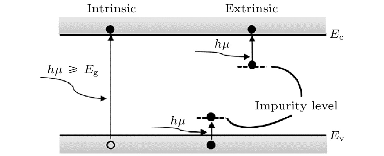
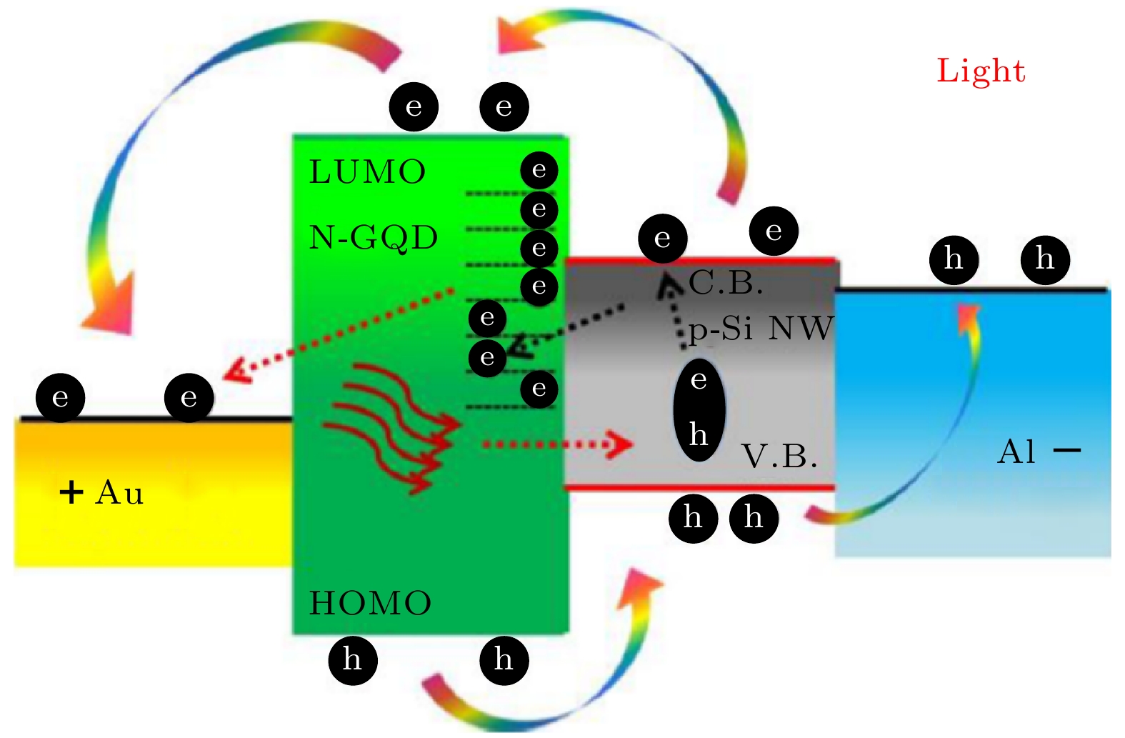
图 3 在光照射下, 硅光敏层中产生光生载流子的原理示意图
Figure 3. Schematic diagram for photogenerated carriers in silicon photosensitive layer under illumination.

-
[1] Li C, Liu D, Dai D 2019 Nanophotonics 8 227
Google Scholar
[2] Adinolfi V, Sargent E H 2017 Nature 542 324
Google Scholar
[3] Lee S H, Kang J S, Kim D 2018 Materials 11 2557
Google Scholar
[4] Margalit N, Xiang C, Bowers S M, Bjorlin A, Blum R, Bowers J E 2021 Appl. Phys. Lett. 118 220501
Google Scholar
[5] Wang Y, Ding K, Sun B, Lee ST, Jie J 2016 Nano Res. 9 72
Google Scholar
[6] Liu C, Guo J, Yu L, Li J, Zhang M, Li H, Shi Y, Dai D 2021 Light Sci. Appl. 10 123
Google Scholar
[7] Zhou J, Xin K, Zhao X, Li D, Wei Z, Xia J 2022 Sci. China Mater. 65 876
Google Scholar
[8] Liu J J, Qu J L, Kirchartz T, Song J 2021 J. Mater. Chem. A 9 20919
Google Scholar
[9] Li C, Zhao J H, Chen Z G 2021 J. Alloy. Compd. 883 160765
Google Scholar
[10] Arjmand T, Legallais M, Nguyen T T T, et al. 2022 Nanomaterials 12 1043
Google Scholar
[11] Donnelly V M, Kornblit A 2013 J. Vac. Sci. Technol. 31 050825
Google Scholar
[12] Huo C, Wang J, Fu H, Li X, Yang Y, Wang H, Mateen A, Farid G, Peng K Q 2020 Adv. Funct. Mater. 30 2005744
Google Scholar
[13] Tian W, Sun H, Chen L, Wangyang P, Chen X, Xiong J, Li L 2019 InfoMat 1 140
Google Scholar
[14] Um H D, Solanki A, Jayaraman A, Gordon R G, Habbal F 2019 ACS Nano 13 11717
Google Scholar
[15] Wang X, Tang Y, Wang W, Zhao H, Song Y, Kang C, Wang K 2022 Nanomaterials 12 1824
Google Scholar
[16] Rasool K, Rafiq M A, Ahmad M, Imran Z, Batool S S, Hasan M M 2013 AIP Adv. 3 082111
Google Scholar
[17] Liu J Y, Wang J J, Lin D H, Wang J, Fu C, Liang F X, Li X, Gu Z P, Wu D, Luo L B 2022 ACS Appl. Mater. Interfaces 14 32341
Google Scholar
[18] Ohmi T, Imaoka T, Kezuka T, Takano J, Kogure M 1993 J. Electrochem. Soc. 140 811
Google Scholar
[19] Morinaga H, Suyama M, Ohmi T 1994 J. Electrochem. Soc. 141 2834
Google Scholar
[20] Kim J S, Morita H, Joo J D, Ohmi T 1997 J. Electrochem. Soc. 144 3275
Google Scholar
[21] Morinaga H, Futatsuki T, Ohmi T, Fuchita E, Oda M, Hayashi C 1995 J. Electrochem. Soc. 142 966
Google Scholar
[22] Peng K, Wu Y, Fang H, Zhong X, Xu Y, Zhu J 2005 Angew. Chem. Int. Edit. 44 2737
Google Scholar
[23] Peng K Q, Hu J J, Yan Y J, Wu Y, Fang H, Xu Y, Lee S T, Zhu J 2006 Adv. Funct. Mater. 16 387
Google Scholar
[24] Peng K, Lu A, Zhang R, Lee S T 2008 Adv. Funct. Mater. 18 3026
Google Scholar
[25] Zhang X G, Collins S D, Smith R L 1989 J. Electrochem. Soc. 136 1561
Google Scholar
[26] Kolasinski K W 2010 J. Phys. Chem. C 114 22098
Google Scholar
[27] Turner D R 1960 J. Electrochem. Soc. 107 810
Google Scholar
[28] Peng K Q, Yan Y J, Gao S P, Zhu J 2002 Adv. Mater. 14 1164
Google Scholar
[29] Koynov S, Brandt M S, Stutzmann M 2006 Appl. Phys. Lett. 88 203107
Google Scholar
[30] Peng K, Fang H, Hu J, Wu Y, Zhu J, Yan Y, Lee S 2006 Chem. Eur. J. 12 7942
Google Scholar
[31] Peng K, Zhu J 2003 J. Electroanal. Chem. 558 35
Google Scholar
[32] Tsujino K, Matsumura M 2005 Electrochem. Solid-St. 8 C193
Google Scholar
[33] Hildreth O J, Fedorov A G, Wong C P 2012 ACS Nano 6 10004
Google Scholar
[34] Chen H, Wang H, Zhang X H, Lee C S, Lee S T 2010 Nano Lett. 10 864
Google Scholar
[35] Kim J, Kim Y H, Choi S H, Lee W 2011 ACS Nano 5 5242
Google Scholar
[36] Chen Y, Li L, Zhang C, Tuan C C, Chen X, Gao J, Wong C P 2017 Nano Lett. 17 1014
Google Scholar
[37] Chen Y, Zhang C, Li L, Tuan C C, Wu F, Chen X, Gao J, Ding Y, Wong C P 2017 Nano Lett. 17 4304
Google Scholar
[38] Huang Z, Fang H, Zhu J 2007 Adv. Mater. 19 744
Google Scholar
[39] Pudasaini P R, Ruiz-Zepeda F, Sharma M, Elam D, Ponce A, Ayon A A 2013 ACS Appl. Mater. Interfaces 5 9620
Google Scholar
[40] Hochbaum A I, Chen R, Delgado R D, Liang W, Garnett E C, Najarian M, Majumdar A, Yang P 2008 Nature 451 163
Google Scholar
[41] Hildreth O J, Brown D, Wong C P 2011 Adv. Funct. Mater. 21 3119
Google Scholar
[42] Wang J, Hu Y, Zhao H, Fu H, Wang Y, Huo C, Peng K Q 2018 Adv. Mater. Interfaces 5 1801132
Google Scholar
[43] Lai R A, Hymel T M, Narasimhan V K, Cui Y 2016 ACS Appl. Mater. Interfaces 8 8875
Google Scholar
[44] Li L, Tuan C C, Zhang C, Chen Y, Lian G, Wong C P 2019 J. Microelectromech. Syst. 28 143
Google Scholar
[45] Li L, Zhao X, Wong C P 2015 ECS J. Solid State Sci. Technol. 4 P337
Google Scholar
[46] Li Y, Shi Z F, Li X J, Shan C X 2019 Chin. Phys. B 28 017803
Google Scholar
[47] Han C, Chen Z, Zhang N, Colmenares J C, Xu Y J 2015 Adv. Funct. Mater. 25 221
Google Scholar
[48] Reddy A L M, Gowda S R, Shaijumon M M, Ajayan P M 2012 Adv. Mater. 24 5045
Google Scholar
[49] Lu W, Lieber C M 2007 Nat. Mater. 6 841
Google Scholar
[50] Li Y, Wang H, Xie L, Liang Y, Hong G, Dai H 2011 J. Am. Chem. Soc. 133 7296
Google Scholar
[51] Kholmanov I N, Domingues S H, Chou H, et al. 2013 ACS Nano 7 1811
Google Scholar
[52] Huang Z G, Lin X X, Zeng Y, et al. 2015 Sol. Energy Mater. Sol. Cells 143 302
Google Scholar
[53] Sivakov V, Andrä G, Gawlik A, Berger A, Plentz J, Falk F, Christiansen S H 2009 Nano Lett. 9 1549
Google Scholar
[54] Wan X, Xu Y, Guo H, et al. 2017 NPJ 2D Mater. Appl. 1 4
Google Scholar
[55] Mokkapati S, Saxena D, Tan H H, Jagadish C 2015 Sci. Rep. 5 15339
Google Scholar
[56] Fountaine K T, Whitney W S, Atwater H A 2014 J. Appl. Phys. 116 153106
Google Scholar
[57] Cao L, White J S, Park J S, Schuller J A, Clemens B M, Brongersma M L 2009 Nat. Mater. 8 643
Google Scholar
[58] Wang B, Leu P W 2012 Opt. Lett. 37 3756
Google Scholar
[59] Wang J J, Fu C, Cheng H Y, Tong X W, Zhang Z X, Wu D, Chen L M, Liang F X, Luo L B 2021 ACS Nano 15 16729
Google Scholar
[60] Nusir A I, Bauman S J, Marie M S, Herzog J B, Manasreh M O 2017 Appl. Phys. Lett. 111 171103
Google Scholar
[61] Luo L B, Zeng L H, Xie C, Yu Y Q, Liang F X, Wu C Y, Wang L, Hu J G 2014 Sci. Rep. 4 3914
Google Scholar
[62] Kim K, Yoon S, Seo M, Lee S, Cho H, Meyyappan M, Baek C K 2019 Nat. Electron. 2 572
Google Scholar
[63] Vasa P, Lienau C 2010 Angew. Chem. Int. Edit. 49 2476
Google Scholar
[64] Schaadt D M, Feng B, Yu E T 2005 Appl. Phys. Lett. 86 063106
Google Scholar
[65] Qi Z, Zhai Y, Wen L, Wang Q, Chen Q, Iqbal S, Chen G, Xu J, Tu Y 2017 Nanotechnology 28 275202
Google Scholar
[66] Huang Y, Liang H, Zhang Y, Yin S, Cai C, Liu W, Jia T 2021 ACS Appl. Nano Mater. 4 1567
Google Scholar
[67] Wang H, Wang F, Xu T, et al. 2021 Nano Lett. 21 7761
Google Scholar
[68] Mao C H, Dubey A, Lee F J, et al. 2021 ACS Appl. Mater. Interfaces 13 4126
Google Scholar
[69] Xie C, Nie B, Zeng L, Liang F X, Wang M Z, Luo L, Feng M, Yu Y, Wu C Y, Wu Y, Yu S H 2014 ACS Nano 8 4015
Google Scholar
[70] Mondal H, Dey T, Basori R 2021 ACS Appl. Nano Mater. 4 11938
Google Scholar
[71] Chandra A, Giri S, Das B, Ghosh S, Sarkar S, Chattopadhyay K K 2021 Appl. Surf. Sci. 548 149256
Google Scholar
[72] Liang W, Wang L, Li Y, Zhang F, Chen X, Wu D, Tian Y, Li X, Shan C, Shi Z 2021 Mater. Today Phys. 18 100398
Google Scholar
[73] Feng B, Pan X, Liu T, Tian S, Wang T, Chen Y 2021 Nano Lett. 21 5655
Google Scholar
[74] Tong X W, Wang J J, Li J X, Hu X F, Wu D, Luo L B 2021 Sensor. Actuat. A-Phys. 322 112625
Google Scholar
[75] Sun K, Jing Y, Park N, Li C, Bando Y, Wang D 2010 J. Am. Chem. Soc. 132 15465
Google Scholar
[76] Hong Q, Cao Y, Xu J, Lu H, He J, Sun J L 2014 ACS Appl. Mater. Interfaces 6 20887
Google Scholar
[77] Cao Y, Zhu J, Xu J, He J, Sun J L, Wang Y, Zhao Z 2014 Small 10 2345
Google Scholar
[78] Das B, Das N S, Sarkar S, Chatterjee B K, Chattopadhyay K K 2017 ACS Appl. Mater. Interfaces 9 22788
Google Scholar
[79] Gong C, Zhang Y, Chen W, Chu J, Lei T, Pu J, Dai L, Wu C, Cheng Y, Zhai T, Li L, Xiong J 2017 Adv. Sci. 4 1700231
Google Scholar
[80] Henning A, Sangwan V K, Bergeron H, et al. 2018 ACS Appl. Mater. Interfaces 10 16760
Google Scholar
[81] Asuo I M, Banerjee D, Pignolet A, Nechache R, Cloutier S G 2021 Phys. Status Solidi R. 15 2000537
Google Scholar
[82] Zhao J, Liu H, Deng L, Bai M, Xie F, Wen S, Liu W 2021 Sensors 21 6146
Google Scholar
[83] Mao J, Zhang B, Shi Y, Wu X, He Y, Wu D, Jie J, Lee C S, Zhang X 2022 Adv. Funct. Mater. 32 2108174
Google Scholar
[84] Lu J, Sheng X, Tong G, Yu Z, Sun X, Yu L, Xu X, Wang J, Xu J, Shi Y, Chen K 2017 Adv. Mater. 29 1700400
Google Scholar
[85] Mihalache I, Radoi A, Pascu R, Romanitan C, Vasile E, Kusko M 2017 ACS Appl. Mater. Interfaces 9 29234
Google Scholar
[86] Zhang M, Wang L, Meng L, et al. 2018 Adv. Opt. Mater. 6 1800077
Google Scholar
[87] Weisse J M, Kim D R, Lee C H, Zheng X 2011 Nano Lett. 11 1300
Google Scholar
[88] Mulazimoglu E, Coskun S, Gunoven M, Butun B, Ozbay E, Turan R, Unalan H E 2013 Appl. Phys. Lett. 103 083114
Google Scholar
[89] Xu Y, Shen H, Yue Z, Wang S, Zhao Q, Wang Z 2022 Surf. Interfaces 33 102288
Google Scholar
[90] Chee K W A, Ghosh B K, Saad I, Hong Y, Xia Q H, Gao P, Ye J, Ding Z J 2022 Nano Energy 95 106899
Google Scholar
[91] Dan Y, Seo K, Takei K, Meza J H, Javey A, Crozier K B 2011 Nano Lett. 11 2527
Google Scholar
[92] Yan J, Ge K, Li H, Yang X, Chen J, Wan L, Guo J, Li F, Xu Y, Song D, Flavel B S, Chen J 2021 Nanoscale 13 11439
Google Scholar


 DownLoad:
Catalog
Metrics
- Abstract views: 15036
- PDF Downloads: 434
- Cited By: 0
