-
Photodetectors are widely used in the fields of environmental monitoring, medical analysis, security surveillance, optical communication and biosensing due to their high responsiveness, fast response time, low power consumption, good stability and low processing cost. Fully inorganic lead-free perovskite material (Cs2AgBiBr6) has received a lot of attention in recent years in the research of photodetector applications due to its advantages of long carrier lifetime, high stability, moderate forbidden bandwidth, and environmental friendliness. For perovskite photodetectors, the semiconductor nanopillar array structure can effectively reduce the reflection loss of light from the surface to improve the absorption of incident light in the device and inhibit the exciton complexes in the device, and the good energy level matching between TiO2 and Cs2AgBiBr6 can effectively promote the transport and extraction of carriers in the device. However, there are few reports on the use of TiO2 nanopillar arrays as a transport layer to improve the performance of Cs2AgBiBr6 photodetectors. In this work, high-quality Cs2AgBiBr6 thin films with large grain size, no visible pinholes, and good uniform coverage are successfully prepared by a low-pressure-assisted spin-coating method under ambient conditions. Hydrothermally grown TiO2 nanopillar arrays are embedded into the Cs2AgBiBr6 layer to form a close core-shell structure, increasing the physical contact area between the two to ensure more effective electron injection and charge separation, and to improve the carrier transport efficiency in the device. Multi-band responsive Cs2AgBiBr6 double perovskite photodetectors based on TiO2 nanopillars are excited at multiple wavelengths of 365 nm and 405 nm with high light response and good stability and reproducibility, resulting in average switching ratios of 522 and 2090, respectively. When the light source is excited at 365 nm and 405 nm with a light intensity of 0.056 W/cm2, the responsivity is 0.019 A/W and 0.057 A/W, respectively, and the specific detectivity is 1.9 × 10¹⁰ Jones and 5.6 × 10¹⁰ Jones, respectively. Comparing with the Cs2AgBiBr6 perovskite photodetector based on a planar TiO2 electron transport layer, the average switching ratios are improved by a factor of 65 and 110, the responsivities are improved by 35% and 256%, and the specific detectivity are improved by a factor of 6.9 and 25, respectively. In this work, the photoelectric performance of Cs2AgBiBr6 photodetector is improved by using TiO2 nanopillars as an electron transport layer. It provides a reference solution for developing high-performance Cs2AgBiBr6 perovskite photodetectors in future.
-
Keywords:
- Cs2AgBiBr6 /
- photodetector /
- TiO2 nanopillars /
- multi band response
[1] Li Z Q, Yan T T, Fang X S 2023 Nat. Rev. Mater. 8 587
 Google Scholar
[2] Arya S, Mahajan P, Gupta R, et al. 2020 Prog. Solid State Chem. 60 100286
 Google Scholar
[3] Chen Y H, Feng Z J, Pal A, Zhang J C 2022 Phys. Status Solidi A-Appl. Mat. 219 2200018
 Google Scholar
[4] Chouhan L, Ghimire S, Subrahmanyam C, Miyasaka T, Biju V 2020 Chem. Soc. Rev. 49 2869
 Google Scholar
[5] Li H Y, Shen N, Chen S, Guo F, Xu B M 2023 Adv. Funct. Mater. 33 32
 Google Scholar
[6] 郤育莺, 韩悦, 李国辉, 翟爱平, 冀婷, 郝玉英, 崔艳霞 2020 物理学报 69 167804
 Google Scholar
Xi Y Y, Han Y, Li G H, Zhai A P, Ji T, Hao Y Y, Cui Y X 2020 Acta Phys. Sin. 69 167804
 Google Scholar
[7] Jeong B, Han H, Park C 2020 Adv. Mater. 32 35
 Google Scholar
[8] Priyadarshini P, Senapati S, Naik R 2023 Renew. Sust. Energ. Rev. 186 39
 Google Scholar
[9] Wang Y X, Zhao H R, Piotrowski M, et al. 2022 Micromachines 13 28
 Google Scholar
[10] Shamsi J, Urban A S, Imran M, De Trizio L, Manna L 2019 Chem. Rev. 119 3296
 Google Scholar
[11] Chang Z Z, Lu Z J, Deng W, Shi Y D, Sun Y Y, Zhang X J, Jie J S 2023 Nanoscale 15 5053
 Google Scholar
[12] Chang Z Z, Deng W, Ren X B, Liu X Y, Luo G, Tan Y, Zhang X J, Jie J S 2023 ACS Appl. Mater. Interfaces 15 32037
 Google Scholar
[13] 王俪璇, 李仁杰, 刘辉, 王鹏阳, 石标, 赵颖, 张晓丹 2021 物理学报 70 118402
 Google Scholar
Wang L X, Li R J, Liu H, Wang P Y, Shi B A, Zhao Y, Zhang X D 2021 Acta Phys. Sin. 70 118402
 Google Scholar
[14] Nazir G, Lee S Y, Lee J H, Rehman A, Lee J K, Il Seok S, Park S J 2022 Adv. Mater. 34 45
 Google Scholar
[15] Yan X B, Zhao Y, Cao G, Li X Y, Gao C, Liu L, Ahmed S, Altaf F, Tan H, Ma X P, Xie Z J, Zhang H 2023 Adv. Sci. 10 55
 Google Scholar
[16] Ghosh S, Pradhan B 2019 Chem. Nano. Mat. 5 300
 Google Scholar
[17] Yan Y J, Pullerits T, Zheng K B, Liang Z Q 2020 ACS Energy Lett. 5 2052
 Google Scholar
[18] Gao Z Y, Mao G Y, Chen S Y, Bai Y, Gao P, Wu C C, Gates I D, Yang W J, Ding X L, Yao J X 2022 Phys. Chem. Chem. Phys. 24 3460
 Google Scholar
[19] Ikram M, Malik R, Raees R, Imran M, Wang F, Ali S, Khan M, Khan Q, Maqbool M 2022 Sustain. Energy Technol. Assess. 53 16
 Google Scholar
[20] Supatutkul C, Sitarachu K, Laosiritaworn Y, Jaroenjittichai A P 2023 Mater. Today Commun. 36 7
 Google Scholar
[21] Igbari F, Xu F F, Shao J Y, Ud-Din F, Siffalovic P, Zhong Y W 2023 Sol. RRL 7 28
 Google Scholar
[22] Chen X, Jia M C, Xu W, Pan G C, Zhu J Y, Tian Y T, Wu D, Li X J, Shi Z F 2023 Adv. Opt. Mater. 11 48
 Google Scholar
[23] Dipta S S, Uddin A, Conibeer G 2022 Heliyon 8 12
 Google Scholar
[24] Peng Y Y, Jiang D Y, Zhao M, Duan Y H, Wei H M, Li H D, Liang Q C, Wang S W 2023 J. Alloy. Compd. 965 8
 Google Scholar
[25] Zhen C, Wu T T, Chen R Z, Wang L Z, Liu G, Cheng H M 2019 ACS Sustain. Chem. Eng. 7 4586
 Google Scholar
[26] Yuan Y, Ji Z, Yan G H, et al. 2021 J. Mater. Sci. Technol. 75 39
 Google Scholar
[27] Sun P, Qu G P, Hu Q K, Ma Y C, Liu H S, Xu Z X, Huang Z F 2022 ACS Appl. Energ. Mater. 5 3568
 Google Scholar
[28] Manjunath V, Bimli S, Shaikh P A, Ogale S B, Devan R S 2022 J. Mater. Chem. C 10 15725
 Google Scholar
[29] Chen C, Zheng S J, Song H W 2021 Chem. Soc. Rev. 50 7250
 Google Scholar
[30] Xiao B, Tan Y, Yi Z J, Luo Y B, Jiang Q H, Yang J Y 2021 ACS Appl. Mater. Interfaces 13 37027
 Google Scholar
[31] Qin K, Dun G H, Li Y Y, et al. 2023 ACS Appl. Mater. Interfaces 15 37640
 Google Scholar
[32] Slavney A H, Hu T, Lindenberg A M, Karunadasa H I 2016 J. Am. Chem. Soc. 138 2138
 Google Scholar
[33] Djokic V R, Marinkovic A D, Petrovic R D, Ersen O, Zafeiratos S, Mitric M, Ophus C, Radmilovic V R, Janackovic D T 2020 ACS Appl. Mater. Interfaces 12 33058
 Google Scholar
[34] Xiao T, Zhao J, Sun P, Li P, Zhang Y K, Zhao N, Ren Z W, Li G, Huang Z F, Zheng Z J 2021 Small 17 10
 Google Scholar
[35] Pan B K, Gu J H, Xu X L, Xiao L B, Zhao J, Zou G F 2021 Nano Res. 14 3431
 Google Scholar
[36] Cen G B, Sheng H G, Wang Z X, Yi L, Sun H C, An Y P, Zhao C X, Mai W J 2023 J. Colloid Interface Sci. 652 34
 Google Scholar
[37] Jubu P R, Yam F K, Igba V M, Beh K P 2020 J. Solid State Chem. 290 121576
 Google Scholar
[38] Zhang Z Y, Sun Q D, Lu Y, Lu F, Mu X L, Wei S H, Sui M L 2022 Nat. Commun. 13 12
 Google Scholar
[39] Igbari F, Wang R, Wang Z K, Ma X J, Wang Q, Wang K L, Zhang Y, Liao L S, Yang Y 2019 Nano Lett. 19 2066
 Google Scholar
[40] Vu N H, Le H V, Cao T M, Pham V V, Le H M, Duc N M 2012 J. Phys. Condes. Matter 24 405501
 Google Scholar
[41] Dharmale N, Chaudhury S, Kar J 2021 ECS J. Solid State Sci. Technol. 10 10
 Google Scholar
[42] Lal M, Sharma P, Ram C 2021 Optik 241 14
 Google Scholar
[43] Shen W H, Jung U, Xian Z P, Jung B, Park J 2022 J. Alloy. Compd. 929 167329
 Google Scholar
[44] Wang C, Zhao F Z, Zhou Z Y, Li X X, He S L, Zhang M L, Zhang D Y, Zhang L C 2022 J. Alloy. Compd. 905 164245
 Google Scholar
[45] 胡紫婷, 舒鑫, 王香, 李跃, 徐闰, 洪峰, 马忠权, 蒋最敏, 徐飞 2022 物理学报 71 116801
 Google Scholar
Hu Z T, Shu X, Wang X, Li Y, Xu R, Hong F, Ma Z Q, Jiang Z M, Xu F 2022 Acta Phys. Sin. 71 116801
 Google Scholar
[46] Li T, Wang J, Gao Z Y, Lü P, Yang Y B, Wu J S, Hong J W, Wang X Y, Zhou Y W 2019 Appl. Phys. Lett. 115 131103
 Google Scholar
[47] Dang Y Y, Tong G Q, Song W T, Liu Z H, Qiu L B, Ono L K, Qi Y B 2020 J. Mater. Chem. C 8 276
 Google Scholar
[48] Wu C C, Du B W, Luo W, et al. 2018 Adv. Opt. Mater. 6 1800811
 Google Scholar
-
图 1 Cs2AgBiBr6/TiO2 SL@NPs光电探测器制备工艺 (a) TiO2 SL的形成; (b) TiO2 NPs的生长; (c) 前驱体溶液和基底的预热处理; (d) 旋涂法沉积Cs2AgBiBr6薄膜; (e) 低压辅助处理; (f) 退火处理; (g) 热蒸镀沉积Au电极; (h) 钙钛矿光电探测器三维结构示意图
Figure 1. Preparation process of Cs2AgBiBr6/TiO2 SL@NPs photodetectors: (a) Formation of TiO2 SL; (b) growth of TiO2 NPs; (c) preheating treatment of precursor solution and substrate; (d) spin-coating method for deposition of Cs2AgBiBr6 thin film; (e) low pressure auxiliary treatment; (f) annealing treatment; (g) thermal vapour deposition of Au electrodes; (h) schematic diagram of three-dimensional structure of perovskite photodetectors.
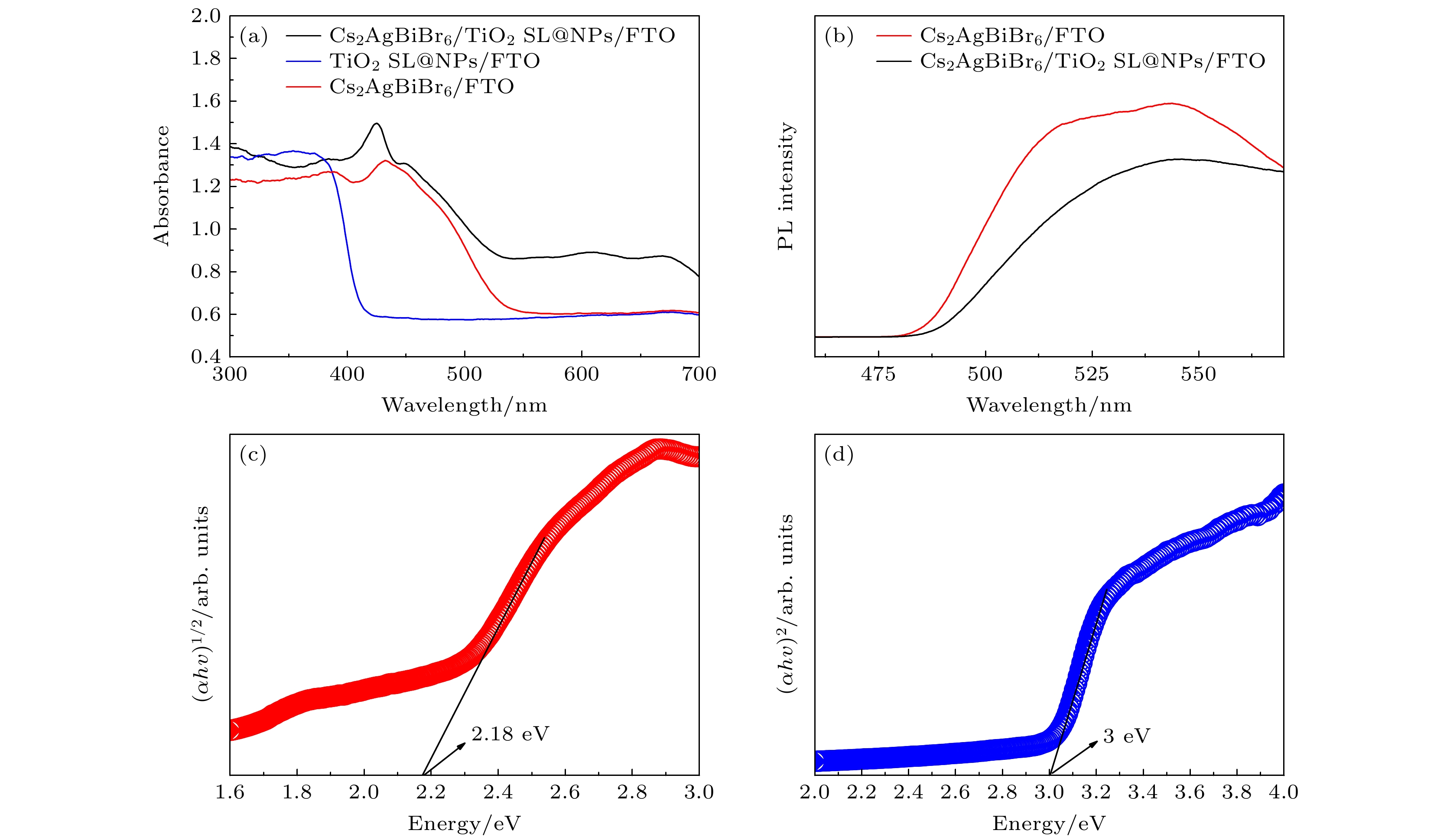
图 5 (a) Cs2AgBiBr6/FTO, TiO2 SL@NPs/FTO和Cs2AgBiBr6/TiO2 SL@NPs/FTO器件的紫外-可见吸收光谱图; (b) Cs2AgBiBr6/FTO, Cs2AgBiBr6/TiO2 SL@NPs/FTO器件的稳态PL光谱图; (c), (d) 分别为Cs2AgBiBr6和TiO2的Tauc图
Figure 5. (a) UV-vis absorption spectra of Cs2AgBiBr6/FTO, TiO2 SL@NPs/FTO and Cs2AgBiBr6/TiO2 SL@NPs/FTO devices; (b) steady-state PL spectra of Cs2AgBiBr6/FTO, Cs2AgBiBr6/TiO2 SL@NPs/FTO devices; (c), (d) Tauc plots for Cs2AgBiBr6 and TiO2, respectively.
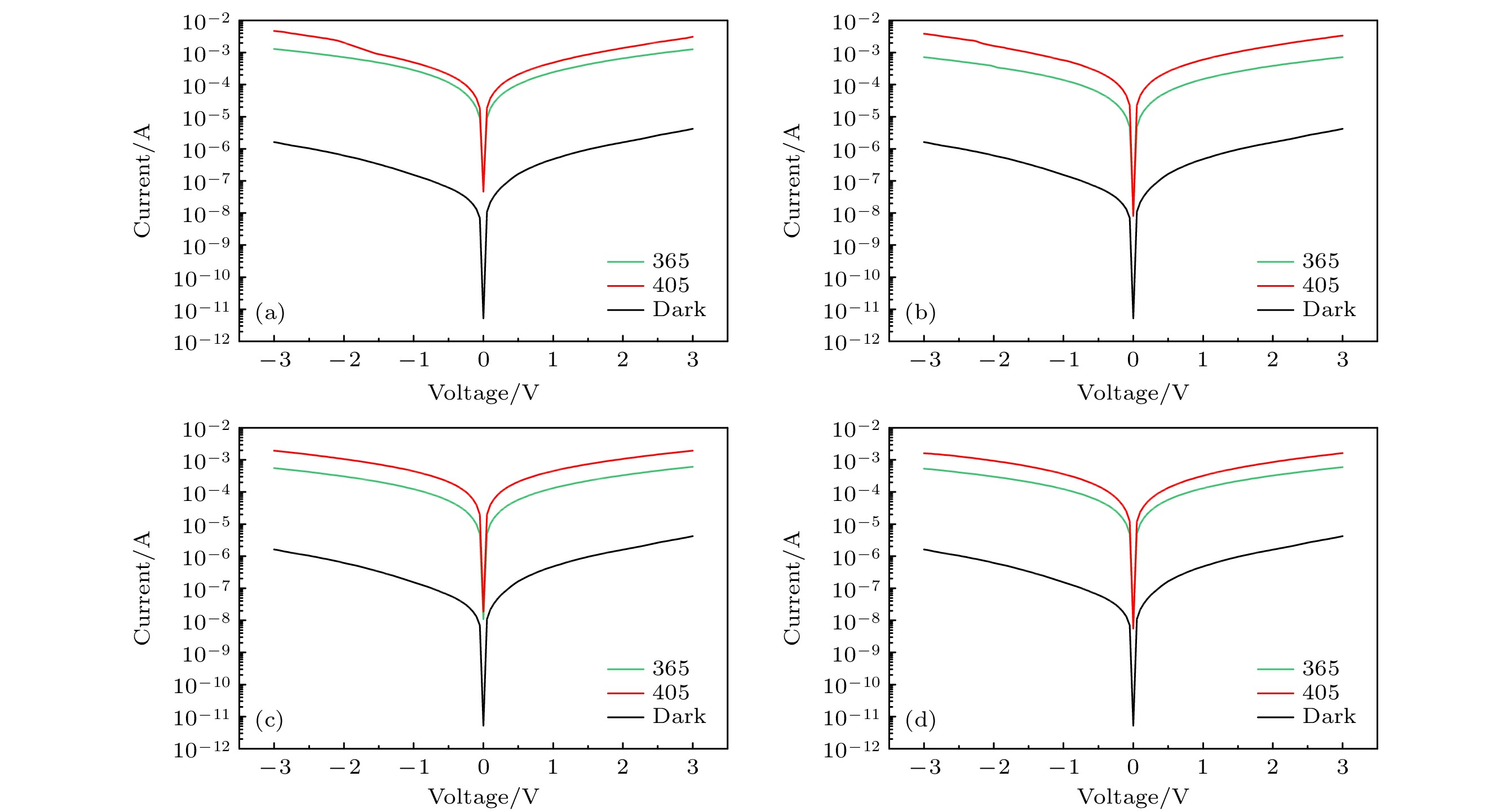
图 6 Cs2AgBiBr6/TiO2 SL@NPs/FTO器件在黑暗条件下所获暗电流值以及被365 nm和405 nm波长光源以不同光功率激发所得光电流值对比 (a) 0.31 W/cm2; (b) 0.152 W/cm2; (c) 0.094 W/cm2; (d) 0.056 W/cm2
Figure 6. Comparison of the dark current values obtained by the Cs2AgBiBr6/TiO2 SL@NPs/FTO device under dark conditions and the photocurrent values obtained by being excited by 365 nm and 405 nm wavelength light sources at different optical power: (a) 0.31 W/cm2; (b) 0.152 W/cm2; (c) 0.094 W/cm2; (d) 0.056 W/cm2.
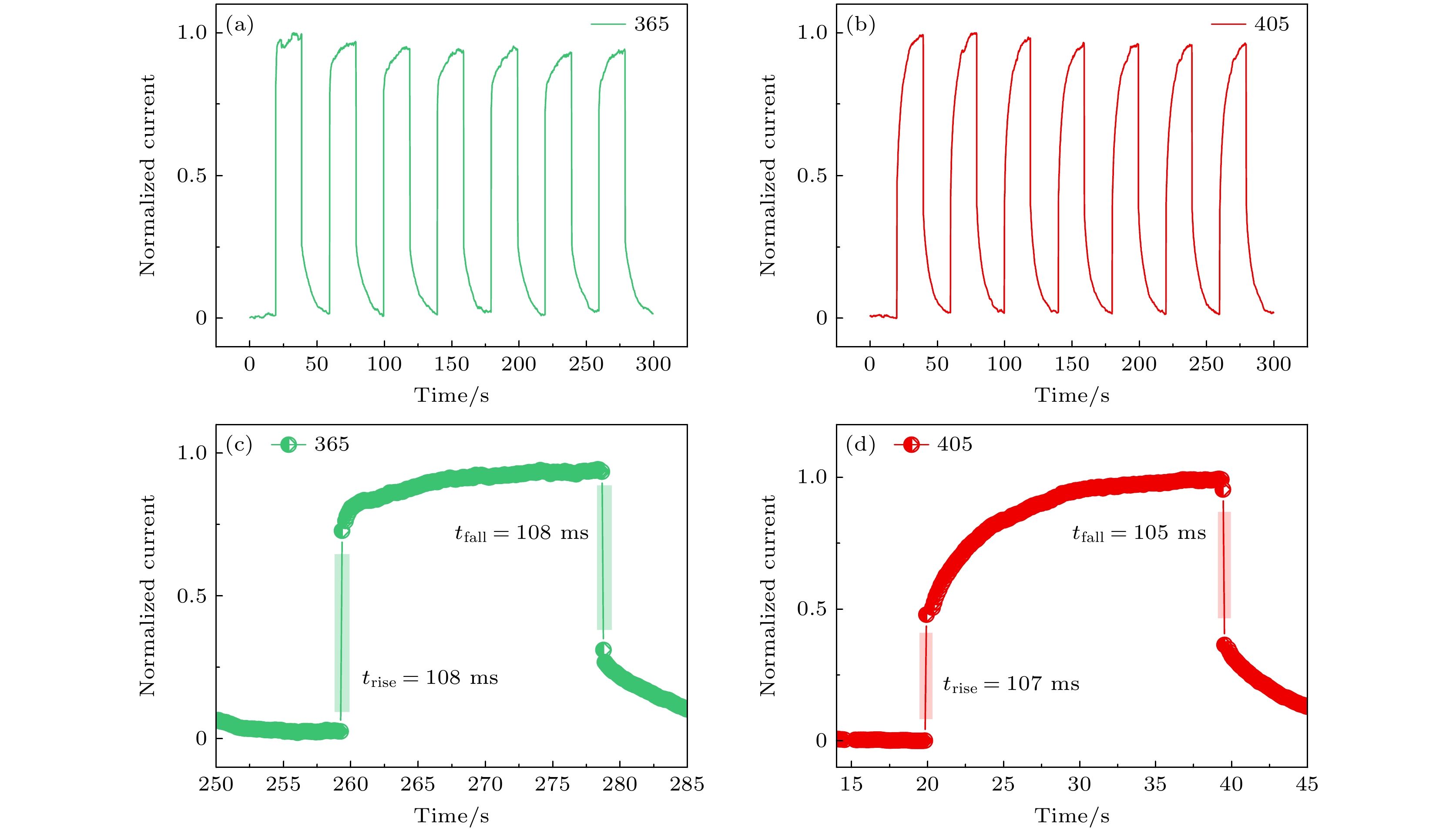
图 7 Cs2AgBiBr6/TiO2 SL@NPs/FTO光电探测器的时域光响应电流(偏压: 0 V、入射光强度: 0.31 W/cm2) (a), (b) 分别为365 nm和405 nm波长光源(开/关)激发的循环I-T曲线图; (c), (d) 分别为365 nm和405 nm波长光源激发的单循环I-T曲线图
Figure 7. Time-domain optical response current of the Cs2AgBiBr6/TiO2 SL@NPs/FTO photodetector (Bias voltage: 0 V, incident light intensity: 0.31 W/cm2): (a), (b) Cyclic I-T curves for the excitation of light source (on/off) at 365 and 405 nm wavelengths, respectively; (c), (d) single-cycle I-T curves for the excitation of light source at 365 and 405 nm wavelengths, respectively.
图 9 Cs2AgBiBr6/TiO2 SL@NPs/FTO光电探测器与Cs2AgBiBr6/TiO2 SL/FTO光电探测器性能指标对比 (a), (b)分别为365 nm和405 nm波长光源以不同光强激发两种器件所获光电流对比以及在黑暗条件下所获暗电流对比; (c), (d)分别为365 nm和405 nm波长光源激发两种器件所获响应度随着入射光强变化的曲线图; (e), (f)分别为365 nm和405 nm波长光源激发两种器件所获比探测率随入射光强变化的曲线图
Figure 9. Comparison of the performance indexes of Cs2AgBiBr6/TiO2 SL@NPs/FTO photodetectors and Cs2AgBiBr6/TiO2 SL/FTO photodetectors: (a), (b) Comparison of photocurrents obtained by exciting the two devices with different light intensities at 365 nm and 405 nm wavelengths, respectively, and the comparison of dark currents obtained under dark conditions; (c), (d) plots of the variation of the responsivity with the incident light intensity obtained by exciting the two devices with 365 nm and 405 nm wavelength light sources, respectively; (e), (f) plots of specific detectivity versus incident light intensity for two devices excited by 365 nm and 405 nm wavelength sources, respectively.
表 1 Cs2AgBiBr6基光电探测器的光响应性能比较
Table 1. Comparison of photoresponse performance of Cs2AgBiBr6-based photodetectors.
Device structure Measurement conditions Responsivity/(A·W–1) D*/(109 Jones) Ref. ITO/Cs2AgBiBr6 single crystal/ITO 1 V, 460 nm 4 × 10⁻⁵ 20 [46] Ag/Cs2AgBiBr6 single crystal 5 V, 400 nm 0.92 1.38 [47] Cs2AgBiBr6/SnO2/ZnO NRs 405 nm 0.608 29.7 [43] Cs2AgBiBr6/SnO2 350 nm 0.11 21 [48] Cs2AgBiBr6/TiO2 SL –3 V, 405 nm 0.016 2.1 This work Cs2AgBiBr6/TiO2 SL –3 V, 365 nm 0.014 2.4 This work Cs2AgBiBr6/TiO2 SL@NPs –3 V, 405 nm 0.057 56 This work Cs2AgBiBr6/TiO2 SL@NPs –3 V, 365 nm 0.019 19 This work -
[1] Li Z Q, Yan T T, Fang X S 2023 Nat. Rev. Mater. 8 587
 Google Scholar
[2] Arya S, Mahajan P, Gupta R, et al. 2020 Prog. Solid State Chem. 60 100286
 Google Scholar
[3] Chen Y H, Feng Z J, Pal A, Zhang J C 2022 Phys. Status Solidi A-Appl. Mat. 219 2200018
 Google Scholar
[4] Chouhan L, Ghimire S, Subrahmanyam C, Miyasaka T, Biju V 2020 Chem. Soc. Rev. 49 2869
 Google Scholar
[5] Li H Y, Shen N, Chen S, Guo F, Xu B M 2023 Adv. Funct. Mater. 33 32
 Google Scholar
[6] 郤育莺, 韩悦, 李国辉, 翟爱平, 冀婷, 郝玉英, 崔艳霞 2020 物理学报 69 167804
 Google Scholar
Xi Y Y, Han Y, Li G H, Zhai A P, Ji T, Hao Y Y, Cui Y X 2020 Acta Phys. Sin. 69 167804
 Google Scholar
[7] Jeong B, Han H, Park C 2020 Adv. Mater. 32 35
 Google Scholar
[8] Priyadarshini P, Senapati S, Naik R 2023 Renew. Sust. Energ. Rev. 186 39
 Google Scholar
[9] Wang Y X, Zhao H R, Piotrowski M, et al. 2022 Micromachines 13 28
 Google Scholar
[10] Shamsi J, Urban A S, Imran M, De Trizio L, Manna L 2019 Chem. Rev. 119 3296
 Google Scholar
[11] Chang Z Z, Lu Z J, Deng W, Shi Y D, Sun Y Y, Zhang X J, Jie J S 2023 Nanoscale 15 5053
 Google Scholar
[12] Chang Z Z, Deng W, Ren X B, Liu X Y, Luo G, Tan Y, Zhang X J, Jie J S 2023 ACS Appl. Mater. Interfaces 15 32037
 Google Scholar
[13] 王俪璇, 李仁杰, 刘辉, 王鹏阳, 石标, 赵颖, 张晓丹 2021 物理学报 70 118402
 Google Scholar
Wang L X, Li R J, Liu H, Wang P Y, Shi B A, Zhao Y, Zhang X D 2021 Acta Phys. Sin. 70 118402
 Google Scholar
[14] Nazir G, Lee S Y, Lee J H, Rehman A, Lee J K, Il Seok S, Park S J 2022 Adv. Mater. 34 45
 Google Scholar
[15] Yan X B, Zhao Y, Cao G, Li X Y, Gao C, Liu L, Ahmed S, Altaf F, Tan H, Ma X P, Xie Z J, Zhang H 2023 Adv. Sci. 10 55
 Google Scholar
[16] Ghosh S, Pradhan B 2019 Chem. Nano. Mat. 5 300
 Google Scholar
[17] Yan Y J, Pullerits T, Zheng K B, Liang Z Q 2020 ACS Energy Lett. 5 2052
 Google Scholar
[18] Gao Z Y, Mao G Y, Chen S Y, Bai Y, Gao P, Wu C C, Gates I D, Yang W J, Ding X L, Yao J X 2022 Phys. Chem. Chem. Phys. 24 3460
 Google Scholar
[19] Ikram M, Malik R, Raees R, Imran M, Wang F, Ali S, Khan M, Khan Q, Maqbool M 2022 Sustain. Energy Technol. Assess. 53 16
 Google Scholar
[20] Supatutkul C, Sitarachu K, Laosiritaworn Y, Jaroenjittichai A P 2023 Mater. Today Commun. 36 7
 Google Scholar
[21] Igbari F, Xu F F, Shao J Y, Ud-Din F, Siffalovic P, Zhong Y W 2023 Sol. RRL 7 28
 Google Scholar
[22] Chen X, Jia M C, Xu W, Pan G C, Zhu J Y, Tian Y T, Wu D, Li X J, Shi Z F 2023 Adv. Opt. Mater. 11 48
 Google Scholar
[23] Dipta S S, Uddin A, Conibeer G 2022 Heliyon 8 12
 Google Scholar
[24] Peng Y Y, Jiang D Y, Zhao M, Duan Y H, Wei H M, Li H D, Liang Q C, Wang S W 2023 J. Alloy. Compd. 965 8
 Google Scholar
[25] Zhen C, Wu T T, Chen R Z, Wang L Z, Liu G, Cheng H M 2019 ACS Sustain. Chem. Eng. 7 4586
 Google Scholar
[26] Yuan Y, Ji Z, Yan G H, et al. 2021 J. Mater. Sci. Technol. 75 39
 Google Scholar
[27] Sun P, Qu G P, Hu Q K, Ma Y C, Liu H S, Xu Z X, Huang Z F 2022 ACS Appl. Energ. Mater. 5 3568
 Google Scholar
[28] Manjunath V, Bimli S, Shaikh P A, Ogale S B, Devan R S 2022 J. Mater. Chem. C 10 15725
 Google Scholar
[29] Chen C, Zheng S J, Song H W 2021 Chem. Soc. Rev. 50 7250
 Google Scholar
[30] Xiao B, Tan Y, Yi Z J, Luo Y B, Jiang Q H, Yang J Y 2021 ACS Appl. Mater. Interfaces 13 37027
 Google Scholar
[31] Qin K, Dun G H, Li Y Y, et al. 2023 ACS Appl. Mater. Interfaces 15 37640
 Google Scholar
[32] Slavney A H, Hu T, Lindenberg A M, Karunadasa H I 2016 J. Am. Chem. Soc. 138 2138
 Google Scholar
[33] Djokic V R, Marinkovic A D, Petrovic R D, Ersen O, Zafeiratos S, Mitric M, Ophus C, Radmilovic V R, Janackovic D T 2020 ACS Appl. Mater. Interfaces 12 33058
 Google Scholar
[34] Xiao T, Zhao J, Sun P, Li P, Zhang Y K, Zhao N, Ren Z W, Li G, Huang Z F, Zheng Z J 2021 Small 17 10
 Google Scholar
[35] Pan B K, Gu J H, Xu X L, Xiao L B, Zhao J, Zou G F 2021 Nano Res. 14 3431
 Google Scholar
[36] Cen G B, Sheng H G, Wang Z X, Yi L, Sun H C, An Y P, Zhao C X, Mai W J 2023 J. Colloid Interface Sci. 652 34
 Google Scholar
[37] Jubu P R, Yam F K, Igba V M, Beh K P 2020 J. Solid State Chem. 290 121576
 Google Scholar
[38] Zhang Z Y, Sun Q D, Lu Y, Lu F, Mu X L, Wei S H, Sui M L 2022 Nat. Commun. 13 12
 Google Scholar
[39] Igbari F, Wang R, Wang Z K, Ma X J, Wang Q, Wang K L, Zhang Y, Liao L S, Yang Y 2019 Nano Lett. 19 2066
 Google Scholar
[40] Vu N H, Le H V, Cao T M, Pham V V, Le H M, Duc N M 2012 J. Phys. Condes. Matter 24 405501
 Google Scholar
[41] Dharmale N, Chaudhury S, Kar J 2021 ECS J. Solid State Sci. Technol. 10 10
 Google Scholar
[42] Lal M, Sharma P, Ram C 2021 Optik 241 14
 Google Scholar
[43] Shen W H, Jung U, Xian Z P, Jung B, Park J 2022 J. Alloy. Compd. 929 167329
 Google Scholar
[44] Wang C, Zhao F Z, Zhou Z Y, Li X X, He S L, Zhang M L, Zhang D Y, Zhang L C 2022 J. Alloy. Compd. 905 164245
 Google Scholar
[45] 胡紫婷, 舒鑫, 王香, 李跃, 徐闰, 洪峰, 马忠权, 蒋最敏, 徐飞 2022 物理学报 71 116801
 Google Scholar
Hu Z T, Shu X, Wang X, Li Y, Xu R, Hong F, Ma Z Q, Jiang Z M, Xu F 2022 Acta Phys. Sin. 71 116801
 Google Scholar
[46] Li T, Wang J, Gao Z Y, Lü P, Yang Y B, Wu J S, Hong J W, Wang X Y, Zhou Y W 2019 Appl. Phys. Lett. 115 131103
 Google Scholar
[47] Dang Y Y, Tong G Q, Song W T, Liu Z H, Qiu L B, Ono L K, Qi Y B 2020 J. Mater. Chem. C 8 276
 Google Scholar
[48] Wu C C, Du B W, Luo W, et al. 2018 Adv. Opt. Mater. 6 1800811
 Google Scholar
Catalog
Metrics
- Abstract views: 7100
- PDF Downloads: 215
- Cited By: 0


 DownLoad:


