


-
A comprehensive van der Waals heterostructure strategy has been implemented to be able to observe all Davydov components of the A-mode in few-layer transition-metal dichalcogenides (TMDs) at room temperature. In few-layer 2H-TMDs such as MoS2, MoSe2, and WS2, the A-mode phonon splits into N Davydov components that directly reflect the interlayer coupling strength and layer number. Under the resonance conditions near the band edge, however, strong photoluminescence (PL) and band filling effects severely obscure these Raman signals, particularly for infrared-active modes, rendering the observation of all the Davydov components at ambient temperature infeasible. In this work, few-layer (1–4 layers) TMD flakes are mechanically exfoliated and dry-transferred onto four-layer graphene, followed by high-vacuum annealing to improve the interfacial coupling quality. Ultralow-frequency Raman spectra of interlayer shear and breathing modes provide an unambiguous fingerprint for determining the layer numbers of both TMDs and graphene constituents, while differential reflectance spectra precisely determine the resonance energies of excitons. Under resonance excitation with the A-exciton, the heterostructures exhibit a marked enhancement of A-mode Raman intensity accompanied by strong PL quenching. Raman peaks associated with all the Davydov components are simultaneously resolved for MoS2, MoSe2, and WS2 at room temperature. The activation of all the Davydov components arises from three synergistic mechanisms: 1) symmetry breaking at the TMDs/graphene interface, which renders the forbidden components Raman-allowed; 2) interfacial charge transfer, which suppresses the PL background by depleting photoexcited carriers entering into graphene; and 3) efficient nonradiative relaxation pathways provided by graphene, which mitigates the band filling effect and restore resonant Raman scattering. Furthermore, the highest-frequency Davydov component A(1) exhibits an overall blue shift in the heterostructure relative to the intrinsic TMDs, with the magnitude of the shift decreasing as the layer number increases. This behavior can be explained by a diatomic linear-chain model in which interfacial van der Waals coupling enhances the force constants of intralayer vibrations. This work thus establishes a general platform for Raman analysis of all the Davydov components of the A mode in two-dimensional (2D) TMDs at room temperature and elucidates how interface coupling, layer number, and symmetry breaking jointly govern phonon behavior. The approach offers valuable insights into phonon engineering and interface design in 2D heterostructures and may readily be extended to relevant systems such as WSe2 and ReS2. -
Keywords:
- Davydov components /
- heterostructures /
- transition metal dichalcogenides /
- interlayer coupling /
- Raman spectroscopy
[1] Splendiani A, Sun L, Zhang Y, Li T, Kim J, Chim C Y, Galli G, Wang F 2010 Nano Lett. 10 1271
 Google Scholar
[2] Wang G, Chernikov A, Glazov M M, Heinz T F, Marie X, Amand T, Urbaszek B 2018 Rev. Mod. Phys. 90 021001
Google Scholar
[3] Zhang X, Qiao X F, Shi W, Wu J B, Jiang D S, Tan P H 2015 Chem. Soc. Rev. 44 2757
Google Scholar
[4] Song Q J, Tan Q H, Zhang X, Wu J B, Sheng B W, Wan Y, Wang X Q, Dai L, Tan P H 2016 Phys. Rev. B 93 115409
Google Scholar
[5] Leng Y C, Lin M L, Zhou Y, Wu J B, Meng D, Cong X, Li H, Tan P H 2021 Nanoscale 13 9732
Google Scholar
[6] Kim K, Lee J U, Nam D, Cheong H 2016 ACS Nano 10 8113
Google Scholar
[7] Tan Q H, Sun Y J, Liu X L, Zhao Y, Xiong Q, Tan P H, Zhang J 2017 2D Mater. 4 031007
Google Scholar
[8] Kim S, Kim K, Lee J, Cheong H 2017 2D Mater. 4 045002
[9] Tan P H 2019 Raman Spectroscopy of Two-Dimensional Materials (Singapore: Springer) pp203–227
[10] 张琼予, 崔旭伟, 董文龙, JARAPANYACHEEP Rapisa, 刘璐琪 2025 光散射学报 37 188
Google Scholar
Zhang Q Y, Cui X W, Dong W L, Jarapanyacheep R, Liu L Q 2025 Chin. J. Light Scatt. 37 188
Google Scholar
[11] 蒋杰, 李聪慧, 姚森浩, 申珅, 冉娜, 张洁 2024 光散射学报 36 305
Google Scholar
Jiang J, Li C H, Yao S H, Shen S, Ran N, Zhang J 2024 Chin. J. Light Scatt. 36 305
Google Scholar
[12] Liu Y, Hu X, Wang T, Liu D 2019 ACS Nano 13 14416
Google Scholar
[13] Shi H, Yan R, Bertolazzi S, Brivio J, Gao B, Kis A, Jena D, Xing H G, Huang L 2013 ACS Nano 7 1072
Google Scholar
[14] Mei R, Zhong Y G, Xie J L, Wu J B, Du W N, Zhang X H, Liu X F, Lin M L, Tan P H 2025 Laser Photonics Rev. e00821
Google Scholar
[15] Jiang Y, Chen S, Zheng W, Zheng B, Pan A 2021 Light Sci. Appl. 10 72
Google Scholar
[16] Li H, Wu J B, Ran F, Lin M L, Liu X L, Zhao Y, Lu X, Xiong Q, Zhang J, Huang W, Zhang H, Tan P H 2017 ACS Nano 11 11714
Google Scholar
[17] Huang Y, Sutter E, Shi N N, Zheng J, Yang T, Englund D, Gao H J, Sutter P 2015 ACS Nano 9 10612
Google Scholar
[18] Castellanos-Gomez A, Buscema M, Molenaar R, Singh V, Janssen L, Van Der Zant H S, Steele G A 2014 2D Mater. 1 011002
Google Scholar
[19] Zhang X, Han W P, Wu J B, Milana S, Lu Y, Li Q Q, Ferrari A C, Tan P H 2013 Phys. Rev. B 87 115413
Google Scholar
[20] Tan P H, Han W P, Zhao W J, Wu Z H, Chang K, Wang H, Wang Y F, Bonini N, Marzari N, Pugno N, Savini G, Lombardo A, Ferrari A C 2012 Nat. Mater. 11 294
Google Scholar
[21] Wu J B, Zhang X, Ijäs M, Han W P, Qiao X F, Li X L, Jiang D S, Ferrari A C, Tan P H 2014 Nat. Commun. 5 5309
Google Scholar
[22] Liang L, Zhang J, Sumpter B G, Tan Q H, Tan P H, Meunier V 2017 ACS Nano 11 11777
Google Scholar
[23] Pierucci D, Henck H, Avila J, Balan A, Naylor C H, Patriarche G, Dappe Y J, Silly M G, Sirotti F, Johnson A T C, Asensio M C, Ouerghi A 2016 Nano Lett. 16 4054
Google Scholar
[24] Bieniek M, Szulakowska L, Hawrylak P 2020 Phys. Rev. B 101 125423
Google Scholar
[25] Robert C, Han B, Kapuscinski P, Delhomme A, Faugeras C, Amand T, Molas M R, Bartos M, Watanabe K, Taniguchi T, Urbaszek B, Potemski M, Marie X 2020 Nat. Commun. 11 4037
Google Scholar
[26] Carvalho B R, Malard L M, Alves J M, Fantini C, Pimenta M A 2015 Phys. Rev. Lett. 114 136403
Google Scholar
[27] Niu Y, Gonzalez-Abad S, Frisenda R, Marauhn P, Drüppel M, Gant P, Schmidt R, Taghavi N S, Barcons D, Molina-Mendoza A J, De Vasconcellos S M, Bratschitsch R, Perez De Lara D, Rohlfing M, Castellanos-Gomez A 2018 Nanomaterials 8 725
Google Scholar
[28] Zhou K G, Withers F, Cao Y, Hu S, Yu G, Casiraghi C 2014 ACS Nano 8 9914
Google Scholar
[29] Tan Q H, Zhang X, Luo X D, Zhang J, Tan P H 2017 J. Semicond. 38 031006
Google Scholar
-
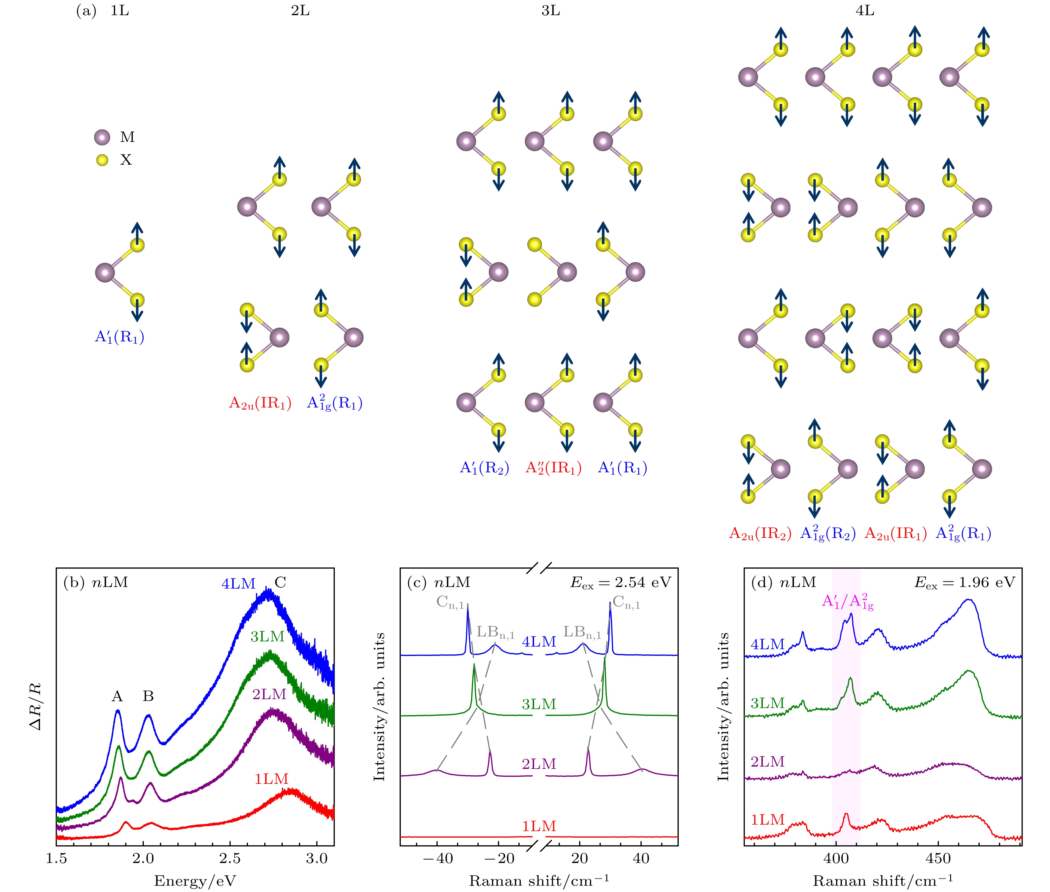
图 1 本征MoS2中A模的Davydov组分 (a) 1—4L TMDs中A模所有Davydov组分原子位移示意图; (b) 本征1—4LM的差分反射谱; (c) 本征1—4LM的低频模; (d) 本征1—4LM中A模的Davydov组分缺失
Figure 1. Davydov components of A-mode in intrinsic MoS2: (a) Schematic diagram of atomic displacements for all the Davydov components of A-mode in 1–4L TMDs; (b) differential reflectance spectra of intrinsic 1–4LM; (c) low-frequency modes of intrinsic 1–4LM; (d) failure to observe all the Davydov components of A-mode in intrinsic 1–4LM.
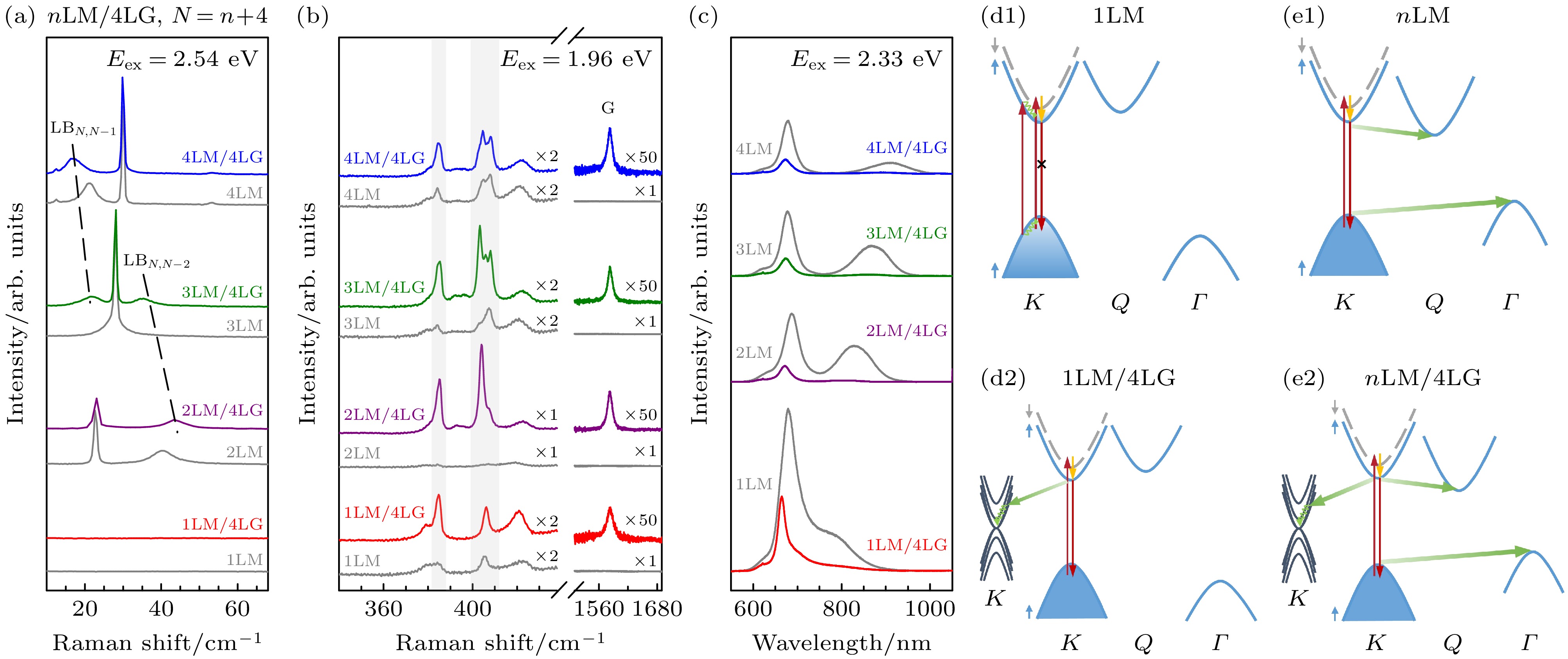
图 2 MoS2/石墨烯异质结的层间耦合与拉曼增强机制 (a) 低频模: nLM/4LG vs. 本征nLM; (b) 高频模: nLM/4LG vs. 本征n LM; (c) PL谱: nLM/4LG vs. 本征nLM. 一阶拉曼增强机制 (d1), (d2) 1LM/4LG vs. 本征1LM; (e1), (e2) nLM/4LG vs. 本征nLM, $ n \geqslant 2 $
Figure 2. Interlayer coupling and Raman enhancement mechanism in MoS2/Gr heterostructures: (a) Low-frequency modes: nLM/4LG vs. intrinsic nLM; (b) high-frequency modes: nLM/4LG vs. intrinsic nLM; (c) PL spectra: nLM/4LG vs. intrinsic nLM. Mechanism of first-order Raman enhancement: (d1), (d2) 1LM/4LG vs. intrinsic 1LM; (e1), (e2) nLM/4LG vs. intrinsic nLM, $ n \geqslant 2 $.
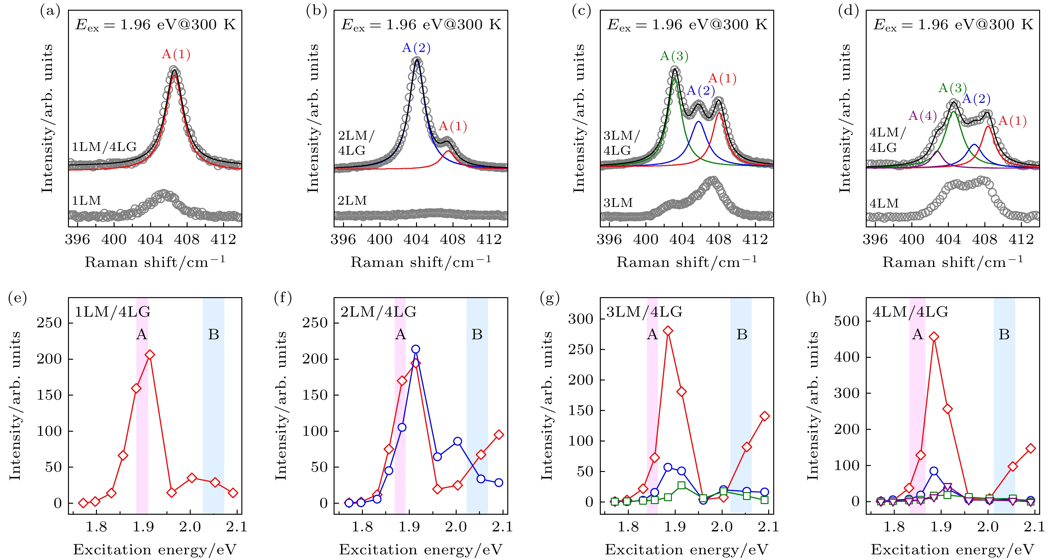
图 3 MoS2/石墨烯异质结中A模的Davydov组分 (a)—(d) 1—4LM/4LG的Davydov组分(室温); (e)—(h) 各组分峰强随激发光能量的变化(1—4LM/4LG)
Figure 3. Davydov components of A-mode in MoS2/Gr heterostructures: (a)–(d) Davydov components in 1–4LM/4LG (room temperature); (e)–(h) Excitation energy dependence of component peak intensities (1–4LM/4LG).
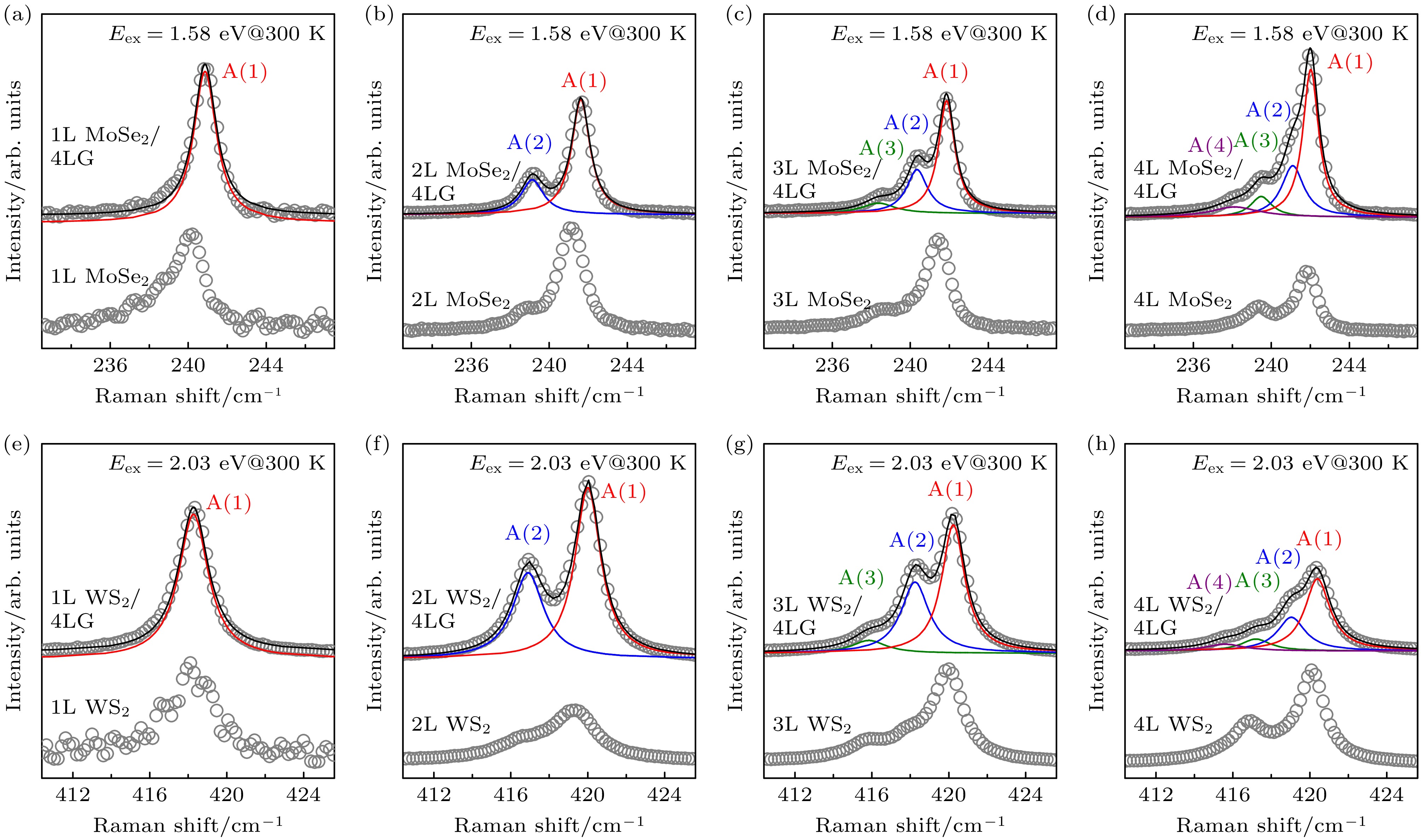
图 4 异质结策略的跨材料普适性 (a)—(d) MoSe2体系与(e)—(h) WS2体系中的Davydov组分观测
Figure 4. Universality of heterostructure strategies. Observation of Davydov components in (a)–(d) MoSe2 system and (e)–(h) WS2 system
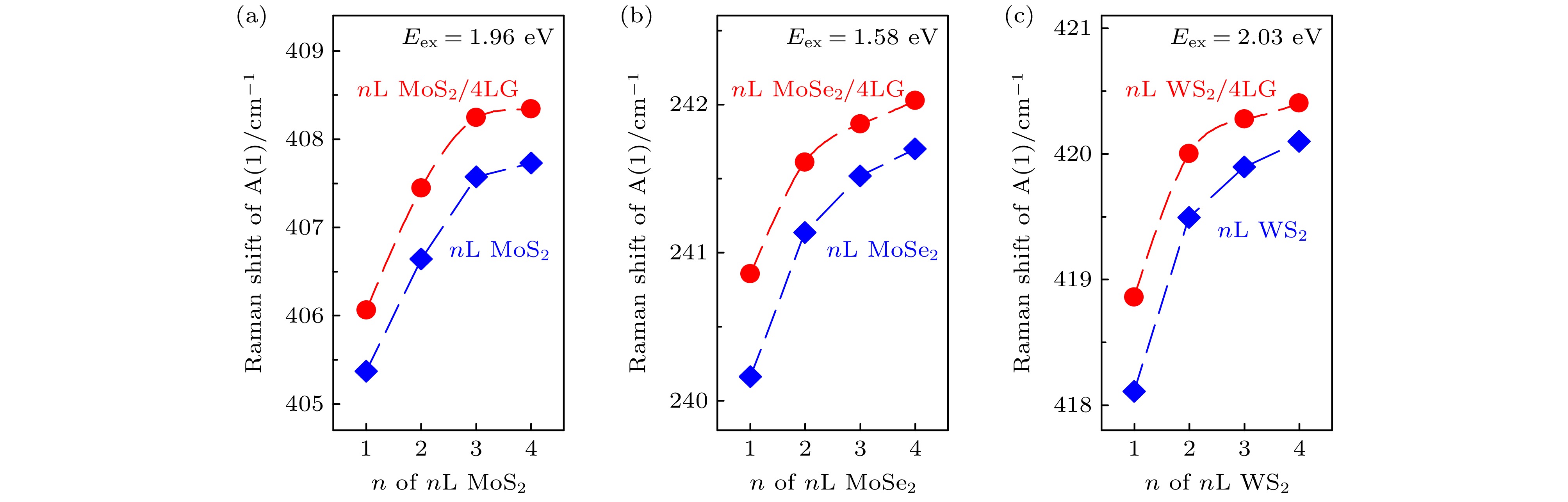
图 5 A(1)模频率的层数依赖关系 (a)—(c) 本征nL MoS2, nL MoSe2, nL WS2样品中A(1)模频率随层数的变化(蓝色菱形); nL MoS2/4LG, nL MoSe2/4LG, nL WS2/4LG异质结样品中A(1)模频率随层数的变化(红色圆形)
Figure 5. Dependence of the Raman peak of A(1) mode on the number of layers (a)–(c) in intrinsic nL MoS2, nL MoSe2, nL WS2 (blue diamond) and in nL MoS2/4LG, nL MoSe2/4LG, nL WS2/4LG heterstructures (red dot).
-
[1] Splendiani A, Sun L, Zhang Y, Li T, Kim J, Chim C Y, Galli G, Wang F 2010 Nano Lett. 10 1271
Google Scholar
[2] Wang G, Chernikov A, Glazov M M, Heinz T F, Marie X, Amand T, Urbaszek B 2018 Rev. Mod. Phys. 90 021001
Google Scholar
[3] Zhang X, Qiao X F, Shi W, Wu J B, Jiang D S, Tan P H 2015 Chem. Soc. Rev. 44 2757
Google Scholar
[4] Song Q J, Tan Q H, Zhang X, Wu J B, Sheng B W, Wan Y, Wang X Q, Dai L, Tan P H 2016 Phys. Rev. B 93 115409
Google Scholar
[5] Leng Y C, Lin M L, Zhou Y, Wu J B, Meng D, Cong X, Li H, Tan P H 2021 Nanoscale 13 9732
Google Scholar
[6] Kim K, Lee J U, Nam D, Cheong H 2016 ACS Nano 10 8113
Google Scholar
[7] Tan Q H, Sun Y J, Liu X L, Zhao Y, Xiong Q, Tan P H, Zhang J 2017 2D Mater. 4 031007
Google Scholar
[8] Kim S, Kim K, Lee J, Cheong H 2017 2D Mater. 4 045002
[9] Tan P H 2019 Raman Spectroscopy of Two-Dimensional Materials (Singapore: Springer) pp203–227
[10] 张琼予, 崔旭伟, 董文龙, JARAPANYACHEEP Rapisa, 刘璐琪 2025 光散射学报 37 188
Google Scholar
Zhang Q Y, Cui X W, Dong W L, Jarapanyacheep R, Liu L Q 2025 Chin. J. Light Scatt. 37 188
Google Scholar
[11] 蒋杰, 李聪慧, 姚森浩, 申珅, 冉娜, 张洁 2024 光散射学报 36 305
Google Scholar
Jiang J, Li C H, Yao S H, Shen S, Ran N, Zhang J 2024 Chin. J. Light Scatt. 36 305
Google Scholar
[12] Liu Y, Hu X, Wang T, Liu D 2019 ACS Nano 13 14416
Google Scholar
[13] Shi H, Yan R, Bertolazzi S, Brivio J, Gao B, Kis A, Jena D, Xing H G, Huang L 2013 ACS Nano 7 1072
Google Scholar
[14] Mei R, Zhong Y G, Xie J L, Wu J B, Du W N, Zhang X H, Liu X F, Lin M L, Tan P H 2025 Laser Photonics Rev. e00821
Google Scholar
[15] Jiang Y, Chen S, Zheng W, Zheng B, Pan A 2021 Light Sci. Appl. 10 72
Google Scholar
[16] Li H, Wu J B, Ran F, Lin M L, Liu X L, Zhao Y, Lu X, Xiong Q, Zhang J, Huang W, Zhang H, Tan P H 2017 ACS Nano 11 11714
Google Scholar
[17] Huang Y, Sutter E, Shi N N, Zheng J, Yang T, Englund D, Gao H J, Sutter P 2015 ACS Nano 9 10612
Google Scholar
[18] Castellanos-Gomez A, Buscema M, Molenaar R, Singh V, Janssen L, Van Der Zant H S, Steele G A 2014 2D Mater. 1 011002
Google Scholar
[19] Zhang X, Han W P, Wu J B, Milana S, Lu Y, Li Q Q, Ferrari A C, Tan P H 2013 Phys. Rev. B 87 115413
Google Scholar
[20] Tan P H, Han W P, Zhao W J, Wu Z H, Chang K, Wang H, Wang Y F, Bonini N, Marzari N, Pugno N, Savini G, Lombardo A, Ferrari A C 2012 Nat. Mater. 11 294
Google Scholar
[21] Wu J B, Zhang X, Ijäs M, Han W P, Qiao X F, Li X L, Jiang D S, Ferrari A C, Tan P H 2014 Nat. Commun. 5 5309
Google Scholar
[22] Liang L, Zhang J, Sumpter B G, Tan Q H, Tan P H, Meunier V 2017 ACS Nano 11 11777
Google Scholar
[23] Pierucci D, Henck H, Avila J, Balan A, Naylor C H, Patriarche G, Dappe Y J, Silly M G, Sirotti F, Johnson A T C, Asensio M C, Ouerghi A 2016 Nano Lett. 16 4054
Google Scholar
[24] Bieniek M, Szulakowska L, Hawrylak P 2020 Phys. Rev. B 101 125423
Google Scholar
[25] Robert C, Han B, Kapuscinski P, Delhomme A, Faugeras C, Amand T, Molas M R, Bartos M, Watanabe K, Taniguchi T, Urbaszek B, Potemski M, Marie X 2020 Nat. Commun. 11 4037
Google Scholar
[26] Carvalho B R, Malard L M, Alves J M, Fantini C, Pimenta M A 2015 Phys. Rev. Lett. 114 136403
Google Scholar
[27] Niu Y, Gonzalez-Abad S, Frisenda R, Marauhn P, Drüppel M, Gant P, Schmidt R, Taghavi N S, Barcons D, Molina-Mendoza A J, De Vasconcellos S M, Bratschitsch R, Perez De Lara D, Rohlfing M, Castellanos-Gomez A 2018 Nanomaterials 8 725
Google Scholar
[28] Zhou K G, Withers F, Cao Y, Hu S, Yu G, Casiraghi C 2014 ACS Nano 8 9914
Google Scholar
[29] Tan Q H, Zhang X, Luo X D, Zhang J, Tan P H 2017 J. Semicond. 38 031006
Google Scholar
-
 20-20250960suppl.pdf


 DownLoad:
Catalog
Metrics
- Abstract views: 1773
- PDF Downloads: 118
- Cited By: 0
