-
石墨烯中等离激元具有特殊的光电性质, 其和入射光的强烈耦合可以引起光吸收的增强. 本文基于时域有限差分法和多体自洽场理论研究了等离激元对处于光学谐振腔中的石墨烯光吸收的影响. 由于石墨烯中等离激元与入射光动量和能量不匹配而不能直接相互作用, 因此石墨烯上施加了金属光栅结构. 研究发现光栅结构能够对入射光进行动量补偿并且能够引起其下石墨烯中的电场强度产生很大程度增强, 从而导致在该石墨烯结构中太赫兹等离激元和入射光发生强烈耦合而产生太赫兹等离极化激元, 同时引起石墨烯光吸收的增强. 希望本文能够加深对石墨烯光电特性的理解以及可以为基于石墨烯的太赫兹光电装置提供一定的理论依据.The plasmons in graphene have the superior properties to metal surface plasmons, such as high field confinement, low Ohmic loss and long wave propagation, highly tunable via electrostatic. More importantly, the frequency of plasmons ranges from terahertz to infrared which indicates that graphene is an ideal candidate for terahertz plamsonics. On the other hand, the strong coupling between incident photons and plasmons in graphene can lead the optical absorption to be enhanced. However, it is difficult for light to couple directly with plasmons in graphene, for the momentum of incident photons cannot match the plasmons in graphene. A metal grating can be used to compensate for the momentum of photons so that it can match that of plasmons in graphene. In this work, we theoretically investigate the effect of plasmons on the terahertz optical absorption of graphene with grating based on finite difference time domain. A great enhancement of electric field component of light field can be obtained near the gold grating strip in the sheet of graphene. Thus, the photons, of which the momentum is compensated for by the grating, can strongly couple with plasmons in graphene. An obviously decrease of the transmission of the graphene structure can be seen at the resonant frequency. The transmission peak corresponds to the resonant frequency spliting into two peaks due to the fact that two plasmon polariton modes are formed by the coupling of photons and palsmons. So we also study the plasmon polariton modes made by coupling photon with palsmon based on the many-body self-consistent method. Two plasmon polariton modes are obtained and an obviously splitting at the resonant frequency can be seen due to the coupling between photons and plasmons. The work conduces to deepening the understanding of the photoelectric properties of graphene and the terahertz plasmonics based on graphene.
-
Keywords:
- graphene /
- plasmon /
- optical absorption /
- plasmon polariton
[1] Castro Neto A H, Guinea F, Peres N M R, Novoselov K S, Geim A K 2009 Rev. Mod. Phys. 81 109
 Google Scholar
[2] Chen J N, Badioli M, Alonso-González P, Thongrattanasiri S, Huth F, Osmond J, Spasenović M, Centeno A, Pesquera A, Godignon P, Elorza A Z, Camara N, García de Abajo F J, Hillenbrand R, Koppens F H L 2012 Nature 487 77
 Google Scholar
[3] Duan J H, Chen R K, Chen J N 2017 Chin. Phys. B 26 117802
 Google Scholar
[4] Ju L, Geng B S, Horng J, Girit C, Martin M, Hao Z, Bechtel H A, Liang X G, Zettl A, Shen Y R, Wang F 2011 Nat. Nanotechnol. 6 630
 Google Scholar
[5] Jablan M, Buljan H, Soljaci M 2009 Phys. Rev. B 80 245435
 Google Scholar
[6] Fei Z, Rodin1A S, Andreev G O, Bao W, McLeod1 A S, Wagner M, Zhang L M, Zhao Z, Thiemens M, Dominguez G, Fogler M M, Castro Neto A H, Lau C N, Keilmann F, Basov D N 2012 Nature 487 82
 Google Scholar
[7] Zhao T, Hu M, Zhong R B, Gong S, Zhang C, Liu S G 2017 Appl. Phys. Lett. 110 231102
 Google Scholar
[8] Liao B X, Guo X D, Hu H, Liu N, Chen K, Yang X X, Dai Q 2018 Chin. Phys. B 27 094101
 Google Scholar
[9] Liu J P, Zhai X, Wang L L, Li F H J, Lin Q, Xia S X 2016 Plasmonics 11 703
 Google Scholar
[10] Jang Y H, Rani A, Quan L N, Adinolfi V, Kanjanaboos P, Ouellette O, Son T, Jang Y J, Chung K W, Kwon H, Kim D, Kim D H, Sargent, E H 2017 ACS Energy Lett. 2 117
 Google Scholar
[11] Ni G X, Wang L, Goldflam M D, Wagner M, Fei Z, McLeod A S, Liu M K, Keilmann F, Özyilmaz B, Castro Neto A H, Hone J, Fogler M M, Basov D N 2016 Nat. Photonics 10 244
 Google Scholar
[12] Nair R R, Blake P, Grigorenko A N, Novoselov K S, Booth T J, Stauber T, Peres N M R, Geim A K 2008 Science 320 1308
 Google Scholar
[13] Gao W L, Shi G, Jin Z H, Shu J, Zhang Q, Vajtai R, Ajayan P M, Kono J, Xu Q F 2013 Nano Lett. 13 3698
 Google Scholar
[14] Zhao C X, Xu W, Li L L, Zhang C, Peeters F M 2015 J. Appl. Phys. 117 223104
 Google Scholar
[15] Lyaschuk Y M, Korotyeyev V V 2012 Ukr. J. Phys. Opt. 13 142
 Google Scholar
[16] Johnson P B, Christy R W 1972 Phys. Rev. B 6 4370
 Google Scholar
[17] Etchegoin P G, Le Ru E C, Meyer M 2006 J. Chem. Phys. 125 164705
 Google Scholar
[18] Kotov O V, Lozovik Y E 2011 Phys. Lett. A 375 2573
 Google Scholar
[19] Yan B, Yang X X, Fang J Y, Huang Y D, Qin H, Qin S Q 2015 Chin. Phys. B 24 015203
 Google Scholar
[20] Yan B, Fang J Y, Qin S Q, Liu Y T, Chen L, Chen S, Li R B, Han Z 2017 Chin. Phys. B 26 097802
 Google Scholar
[21] Yan H G, Li X S, Chandra B, Tulevski G, Wu Y Q, Freitag M, Zhu W J, Avouris P, Xia F N 2012 Nat. Nanotechnol 7 330
 Google Scholar
[22] Dong H M, Li L L, Wang W Y, Zhang S H, Zhao C X, Xu W 2012 Physica E 44 1889
 Google Scholar
[23] Huang Y D, Qin H, Zhang B S, Wu J B, Zhou G C, Jin B B 2013 Appl. Phys. Lett. 102 253106
 Google Scholar
[24] Chaplik A V 1972 Sov. Phys. JETP 35 395
[25] Hwang E H, Das Sarma S 2007 Phys. Rev. B 75 205418
 Google Scholar
[26] Mo S D, Ching W Y 1998 Phys. Rev. B 57 15219
 Google Scholar
[27] Shur M 2010 Electron. Lett. 46 S18
 Google Scholar
[28] Dong H M, Zhang J, Peeters F M, Xu W 2009 J. Appl. Phys. 106 043103
 Google Scholar
[29] Hwang E H, Sarma S Das 2008 Phys. Rev. B 77 195412
 Google Scholar
-
图 1 基于石墨烯的装置示意图(从上至下依次是金光栅/Al2O3薄膜/石墨烯/SiO2/Si; d和w分别代表光栅的周期和光栅条的宽度; 虚线框内的结构可以充当谐振腔的作用; L是谐振腔的厚度)
Fig. 1. Schematic illustration of the device based on graphene. From top to bottom, there are the gold grating layer, Al2O3 dielectric medium, graphene sheet, and SiO2/Si layer. Here, d and w are respectively the period and the width of the gold strips. The structure sketched by the dotted line can be served as cavity and L is the cavity length.
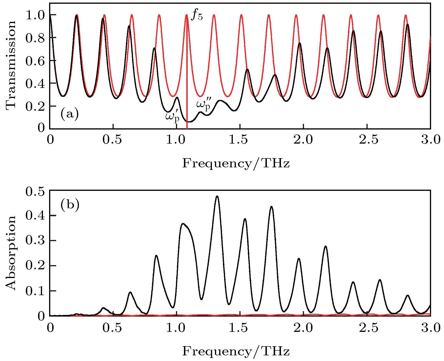
图 2 (a)存在(黑色实线)和不存在(红色实线)石墨烯时的结构透射谱; (b)存在(黑色实线)和不存在(红色实线)石墨烯时的结构吸收谱
Fig. 2. (a) Frequency dependence of the light transmission of the structure with (black solid line) and without graphene (red solid line); (b) frequency dependence of the light absorption of the structure with (black solid line) and without graphene (red solid line).
-
[1] Castro Neto A H, Guinea F, Peres N M R, Novoselov K S, Geim A K 2009 Rev. Mod. Phys. 81 109
 Google Scholar
[2] Chen J N, Badioli M, Alonso-González P, Thongrattanasiri S, Huth F, Osmond J, Spasenović M, Centeno A, Pesquera A, Godignon P, Elorza A Z, Camara N, García de Abajo F J, Hillenbrand R, Koppens F H L 2012 Nature 487 77
 Google Scholar
[3] Duan J H, Chen R K, Chen J N 2017 Chin. Phys. B 26 117802
 Google Scholar
[4] Ju L, Geng B S, Horng J, Girit C, Martin M, Hao Z, Bechtel H A, Liang X G, Zettl A, Shen Y R, Wang F 2011 Nat. Nanotechnol. 6 630
 Google Scholar
[5] Jablan M, Buljan H, Soljaci M 2009 Phys. Rev. B 80 245435
 Google Scholar
[6] Fei Z, Rodin1A S, Andreev G O, Bao W, McLeod1 A S, Wagner M, Zhang L M, Zhao Z, Thiemens M, Dominguez G, Fogler M M, Castro Neto A H, Lau C N, Keilmann F, Basov D N 2012 Nature 487 82
 Google Scholar
[7] Zhao T, Hu M, Zhong R B, Gong S, Zhang C, Liu S G 2017 Appl. Phys. Lett. 110 231102
 Google Scholar
[8] Liao B X, Guo X D, Hu H, Liu N, Chen K, Yang X X, Dai Q 2018 Chin. Phys. B 27 094101
 Google Scholar
[9] Liu J P, Zhai X, Wang L L, Li F H J, Lin Q, Xia S X 2016 Plasmonics 11 703
 Google Scholar
[10] Jang Y H, Rani A, Quan L N, Adinolfi V, Kanjanaboos P, Ouellette O, Son T, Jang Y J, Chung K W, Kwon H, Kim D, Kim D H, Sargent, E H 2017 ACS Energy Lett. 2 117
 Google Scholar
[11] Ni G X, Wang L, Goldflam M D, Wagner M, Fei Z, McLeod A S, Liu M K, Keilmann F, Özyilmaz B, Castro Neto A H, Hone J, Fogler M M, Basov D N 2016 Nat. Photonics 10 244
 Google Scholar
[12] Nair R R, Blake P, Grigorenko A N, Novoselov K S, Booth T J, Stauber T, Peres N M R, Geim A K 2008 Science 320 1308
 Google Scholar
[13] Gao W L, Shi G, Jin Z H, Shu J, Zhang Q, Vajtai R, Ajayan P M, Kono J, Xu Q F 2013 Nano Lett. 13 3698
 Google Scholar
[14] Zhao C X, Xu W, Li L L, Zhang C, Peeters F M 2015 J. Appl. Phys. 117 223104
 Google Scholar
[15] Lyaschuk Y M, Korotyeyev V V 2012 Ukr. J. Phys. Opt. 13 142
 Google Scholar
[16] Johnson P B, Christy R W 1972 Phys. Rev. B 6 4370
 Google Scholar
[17] Etchegoin P G, Le Ru E C, Meyer M 2006 J. Chem. Phys. 125 164705
 Google Scholar
[18] Kotov O V, Lozovik Y E 2011 Phys. Lett. A 375 2573
 Google Scholar
[19] Yan B, Yang X X, Fang J Y, Huang Y D, Qin H, Qin S Q 2015 Chin. Phys. B 24 015203
 Google Scholar
[20] Yan B, Fang J Y, Qin S Q, Liu Y T, Chen L, Chen S, Li R B, Han Z 2017 Chin. Phys. B 26 097802
 Google Scholar
[21] Yan H G, Li X S, Chandra B, Tulevski G, Wu Y Q, Freitag M, Zhu W J, Avouris P, Xia F N 2012 Nat. Nanotechnol 7 330
 Google Scholar
[22] Dong H M, Li L L, Wang W Y, Zhang S H, Zhao C X, Xu W 2012 Physica E 44 1889
 Google Scholar
[23] Huang Y D, Qin H, Zhang B S, Wu J B, Zhou G C, Jin B B 2013 Appl. Phys. Lett. 102 253106
 Google Scholar
[24] Chaplik A V 1972 Sov. Phys. JETP 35 395
[25] Hwang E H, Das Sarma S 2007 Phys. Rev. B 75 205418
 Google Scholar
[26] Mo S D, Ching W Y 1998 Phys. Rev. B 57 15219
 Google Scholar
[27] Shur M 2010 Electron. Lett. 46 S18
 Google Scholar
[28] Dong H M, Zhang J, Peeters F M, Xu W 2009 J. Appl. Phys. 106 043103
 Google Scholar
[29] Hwang E H, Sarma S Das 2008 Phys. Rev. B 77 195412
 Google Scholar
计量
- 文章访问数: 15643
- PDF下载量: 371
- 被引次数: 0


 下载:
下载:


