-
With the advent of graphene, atomically thin two-dimensional materials receive great attention in both science and technology. However, the characterization of zero-band gap of graphene hinders its applications in semiconductor logic and memory devices. To make up for the imperfection of graphene, one has made efforts to search for other two-dimensional layered materials. The Bi2O2Se is an emerging material with very high electron mobility, modest bandgap, and excellent thermal and chemical stability. In this work, high-quality Bi2O2Se thin films are synthesized through chemical vapor deposition. The effect of temperature on the morphology and size distribution of Bi2O2Se thin film are discussed in detail experimentally. Under an optimized experimental condition, the Bi2O2Se thin films with a lateral size of 100 μm are achieved. Interestingly, Bi2O2Se nanowires are obtained at a lower growth temperature (620–640 ℃). The photoelectric performances of Bi2O2Se on mica and silicon oxide substrate are examined based on a photoconductive mode. At a small bias of 0.5 V, the responsivity and specific detectivity of the rectangular Bi2O2Se thin film on the mica substrate reach 45800 A/W and 2.65 × 10¹² Jones, respectively, and the corresponding photoelectric gain is greater than 105. The photoelectric performance of our device is comparable to the best results achieved by other research groups, which may be related to the higher quality and appropriate absorption thickness. The Bi2O2Se nanowire and Bi2O2Se thin film transferred to Si/SiO2 by a polystyrene-assisted method also exhibit a good photoresponse under the illumination of a 532 nm laser with a high optical power density (127.4 mW/cm2). The experimental results demonstrate that the Bi2O2Se has great potential applications in the optoelectronic devices with low power consumption and high sensitivity.
-
Keywords:
- two-dimensional material /
- Bi2O2Se /
- chemical vapor deposition /
- photoconductor
[1] Fu Q, Yang L, Wang W H, Han A L, Huang J, Du P W, Fan Z Y, Zhang J Y, Xiang B 2015 Adv. Mater. 27 4732
 Google Scholar
[2] Mak K F, Lee C G, Hone J, Shan J, Heinz T F 2010 Phys.Rev. Lett. 105 136805
 Google Scholar
[3] 武佩, 胡潇, 张健, 孙连峰 2017 物理学报 66 218102
 Google Scholar
Wu P, Hu X, Zhang J, Sun L F 2017 Acta Phys. Sin. 66 218102
 Google Scholar
[4] Tongay S, Zhou J, Ataca C, Lo K, Matthews T S, Li J B, Grossman J C, Wu J Q 2012 Nano Lett. 12 5576
 Google Scholar
[5] Li B, Huang L, Zhong M, Li Y, Wang Y, Li J B, Wei Z M 2016 Adv. Electron. Mater. 2 1600298
 Google Scholar
[6] 黄林泉, 周玲玉, 于为, 杨栋, 张坚, 李灿 2015 物理学报 64 038103
 Google Scholar
Huang L Q, Zhou L Y, Yu W, Yang D, Zhang J, Li C 2015 Acta Phys. Sin. 64 038103
 Google Scholar
[7] Fu Q D, Zhu C, Zhao X X, et al. 2019 Adv. Mater. 31 1804945
 Google Scholar
[8] Tian X L, Luo H Y, Wei R F, et al. 2018 Adv. Mater. 30 1801021
 Google Scholar
[9] Yin J B, Tan Z J, Hong H, et al. 2018 Nat. Commun. 9 3311
 Google Scholar
[10] Wu J X, Qiu C G, Fu H X, et al. 2019 Nano Lett. 19 197
 Google Scholar
[11] Wu J X, Yuan H T, Meng M M, et al. 2017 Nat. Nanotechnol. 12 530
 Google Scholar
[12] Tong T, Chen Y F, Qin S C, et al. 2019 Adv. Funct. Mater. 29 1905806
 Google Scholar
[13] Liu X L, Li R P, Hong C Y, Huang G F, Pan D F, Ni Z H, Huang Y Q, Ren X M, Cheng Y C, Huang W 2019 Nanoscale 11 20707
 Google Scholar
[14] Luo P, Zhu Ge F W, Wang F K, Lian L Y, Liu K L, Zhang J B, Zhai T Y 2019 ACS Nano 13 9028
 Google Scholar
[15] Wu J X, Liu Y J, Tan Z J, Tan C W, Yin J B, Li T R, Tu T, Peng H L 2017 Adv. Mater. 29 1704060
 Google Scholar
[16] Zhang C C, Wu J X, Sun Y W, Tan C W, Li T R, Tu T, Zhang Y C, Liang Y, Zhou X H, Gao P, Peng H L 2020 J. Am. Chem. Soc. 142 2726
 Google Scholar
[17] Wu J X, Tan C W, Tan Z J, Liu Y J, Yin J B, Dang W H, Wang M Z, Peng H L 2017 Nano Lett. 17 3021
 Google Scholar
[18] Wu Z, Liu G L, Wang Y X, Yang X, Wei T Q, Wang Q J, Liang J, Xu N, Li Z Z, Zhu B, Qi H S, Deng Y, Zhu J 2019 Adv. Funct. Mater. 29 1906639
 Google Scholar
[19] Li J, Wang Z X, Wen Y, Chu J W, Yin L, Cheng R Q, Lei L, He P, Jiang C, Feng L P, He J 2018 Adv. Funct. Mater. 28 1706437
 Google Scholar
[20] Li J, Wang Z X, Chu J W, Cheng Z Z, He P, Wang J J, Yin L, Cheng R Q, Li N N, Wen Y, He J 2019 Appl. Phys. Lett. 114 151104
 Google Scholar
[21] Cheng T, Tan C, Zhang S Q, Teng Tu, Peng H L, Liu Z R 2018 J. Phys. Chem. C 122 19970
 Google Scholar
[22] Pereira A L J, Santamaría-Pérez D, Ruiz-Fuertes J, et al. 2018 J. Phys. Chem. C 122 8853
 Google Scholar
[23] Kufer D, Konstantatos G 2015 Nano Lett. 15 7307
 Google Scholar
[24] Liu E, Long M S, Zeng J W, et al. 2016 Adv. Funct. Mater. 26 1938
 Google Scholar
[25] Huan Y, Zhan X Y, Xu K, Yin L, Cheng Z Z, Jiang C, Wang Z X, He J 2016 Appl. Phys. Lett. 108 013101
 Google Scholar
[26] Zhou X, Gan L, Tian W M, Zhang Q, Jin S Y, Li H Q, Bando Y, Golberg D, Zhai T Y 2015 Adv. Mater. 27 8035
 Google Scholar
[27] Jacobs-Gedrim R B, Shanmugam M, Jain N, Durcan C A, Murphy M T, Murray T M, Matyi R J, Moore R L II, Yu B 2014 ACS Nano 8 514
 Google Scholar
[28] Li X M, Zhu M, Du M D, Lv Z, Zhang L, Li Y C, Yang Y, Yang T T, Li X, Wang K L, Zhu H W, Fang Y 2016 Small 12 595
 Google Scholar
[29] Yuan H T, Liu X G, Afshinmanesh F, Li W, Xu G, Sun J, Lian B, G. Curto A, Ye G J, Hikita Y, Shen Z X, Zhang S C, Chen X H, Brongersma M, Hwang H, Cui Y 2015 Nat. Nanotechnol. 10 707
 Google Scholar
[30] Yu Z R, Aceves-Mijares M, Luna J A L, Deng J X 2009 Proc. SPIE 7381 73811H
 Google Scholar
-
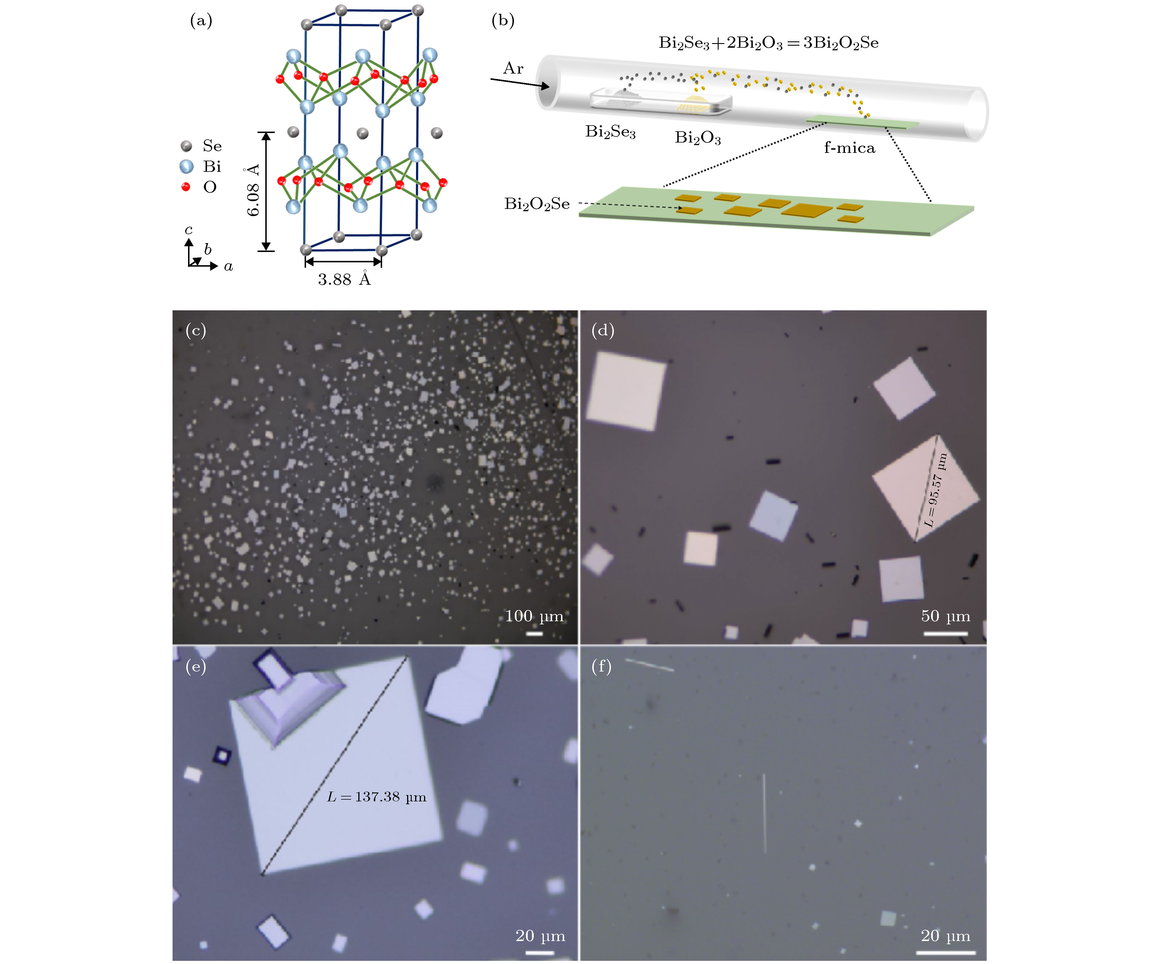
图 1 (a) 层状Bi2O2Se晶体结构示意图; (b) CVD法合成Bi2O2Se实验装置示意图; (c)—(e) 云母上Bi2O2Se薄膜不同放大倍数的光学照片; (f)云母上Bi2O2Se纳米线光学照片
Figure 1. (a) Schematic diagram of the layered Bi2O2Se crystal structure; (b) schematic diagram of the CVD experimental setup for synthesis of Bi2O2Se film; (c)–(e) optical images of Bi2O2Se thin films grown on mica at different magnifications; (f) optical image of Bi2O2Se nanowires grown on mica.
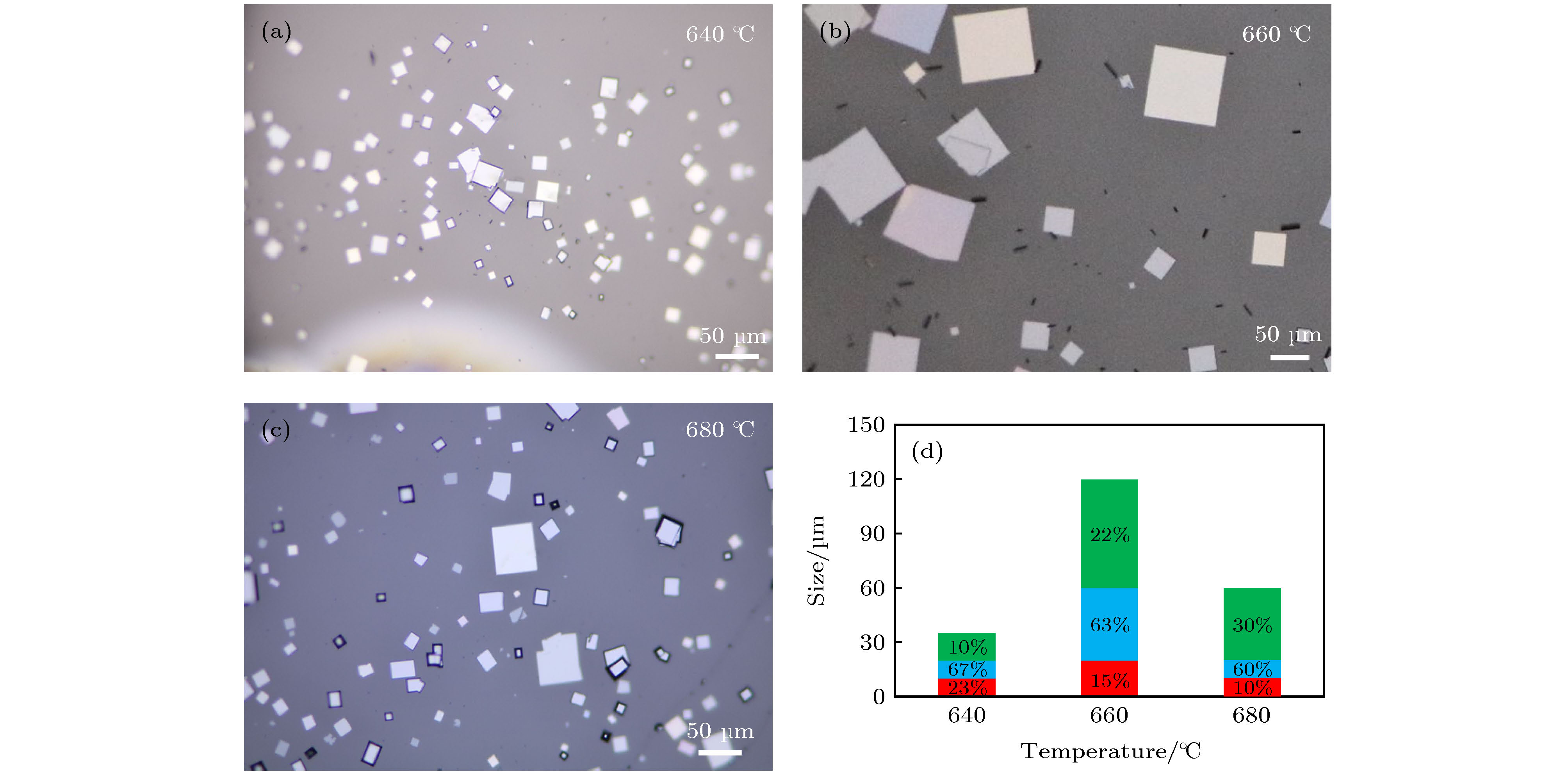
图 2 生长温度对Bi2O2Se薄膜形貌及尺寸分布的影响 (a)—(c) 不同生长温度下云母上Bi2O2Se薄膜的光学照片; (d) 不同生长温度下Bi2O2Se的尺寸分布图, 不同颜色代表不同尺寸范围的Bi2O2Se
Figure 2. Effect of growth temperature on the morphology and the size distribution of Bi2O2Se films: (a)–(c) Optical images of Bi2O2Se thin films grown at 640, 660, 680 ℃, respectively; (d) size distribution of Bi2O2Se films prepared at different growth temperatures. Different color denotes different size range.
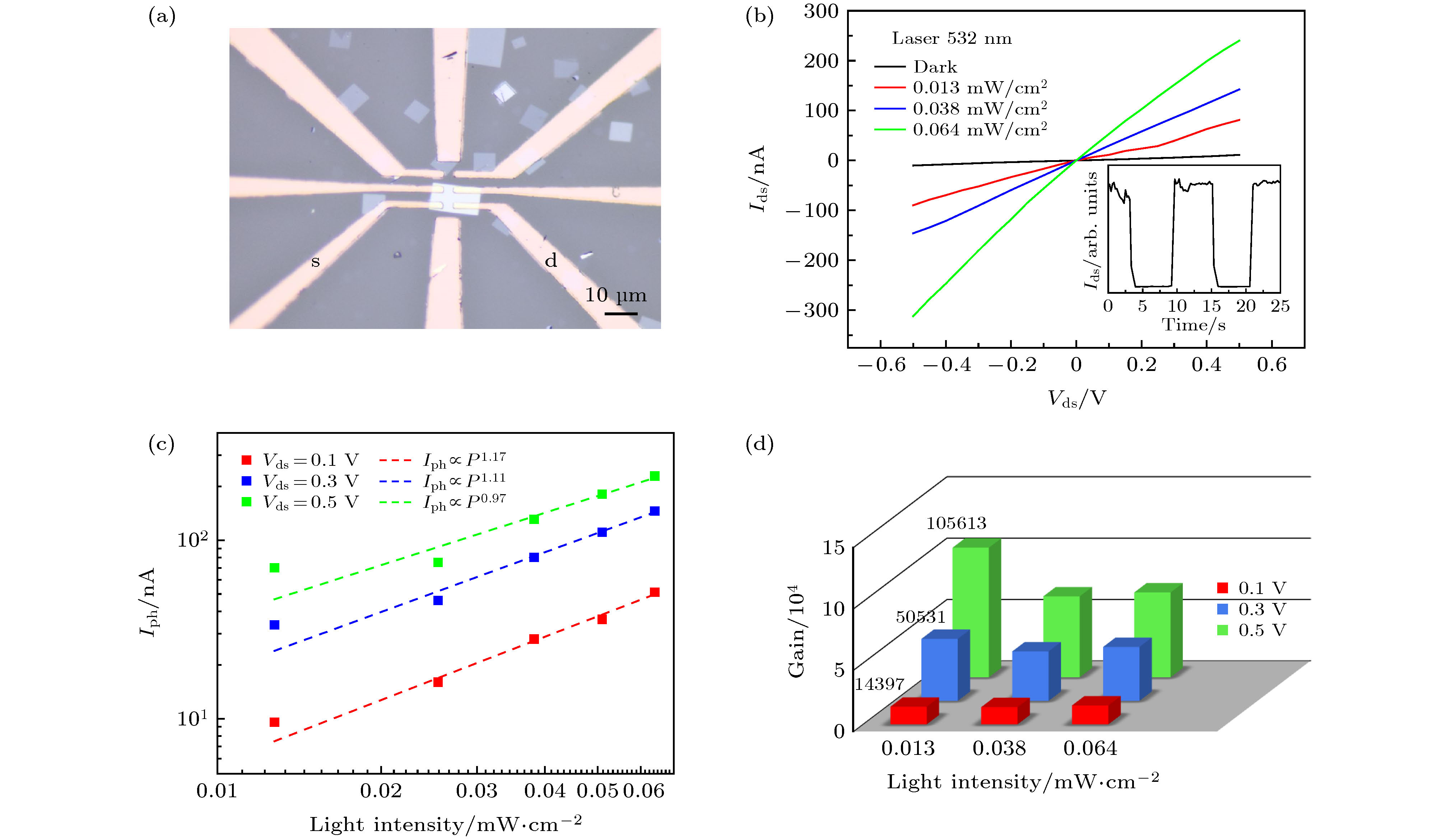
图 4 (a)云母片上Bi2O2Se光电导器件的光学图像; (b)不同光功率密度下Bi2O2Se 器件的Ids-Vds曲线, 插图为器件时间响应的方波图; (c)不同偏置电压条件下, 光电流(Iph)与光功率密度的关系; (d)不同偏置电压条件下, 光增益与光功率密度的关系
Figure 4. (a) Optical image of a Bi2O2Se photoconductive detector on mica; (b) Ids-Vds curves of Bi2O2Se device under illumination by laser with different optical powers; (c) light power dependence of photocurrent (Iph) under different bias; (d) relationship between light gain and light power under different bias.
图 5 (a) 不同光功率下Bi2O2Se纳米线光电探测器的Ids-Vds曲线, 插图为器件光学图像; (b) 在不同入射光功率密度下器件的响应度和比探测率
Figure 5. (a) Ids-Vds curves of Bi2O2Se nanowire photodetector on mica under different light powers. Inset is an optical image of the device. (b) Responsivity and specific detectivity of the device at different light powers.
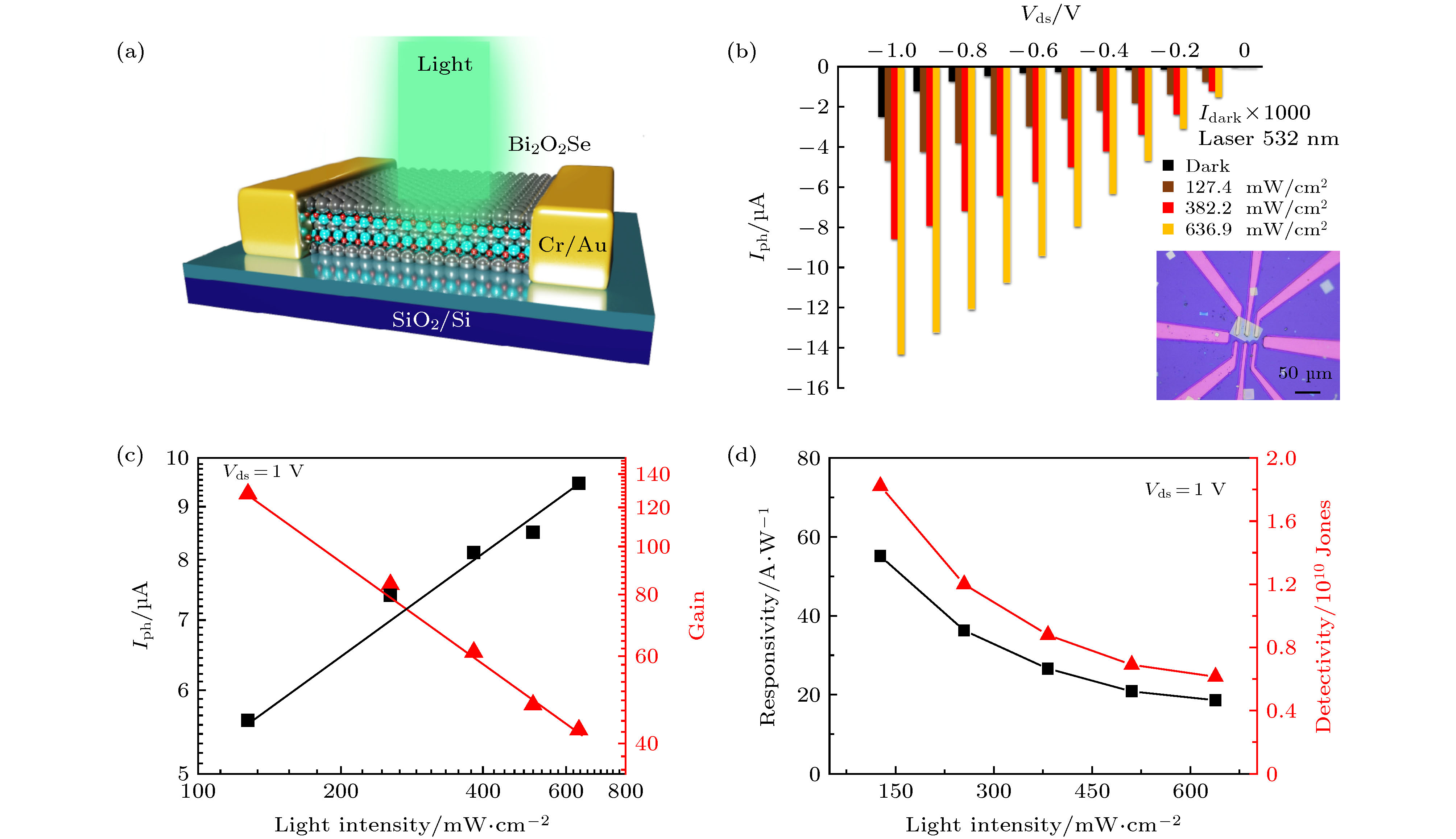
图 6 (a) Si/SiO2衬底上的Bi2O2Se器件示意图; (b) 不同光功率下Bi2O2Se探测器的Ids-Vds行为, 插图为器件的光学图像; (c) Iph、光增益与光源功率密度的关系; (d) Bi2O2Se探测器的响应度和比探测率对光源功率密度的依赖关系
Figure 6. (a) Schematic diagram of the Bi2O2Se photodetector on a Si/SiO2 substrate; (b) Ids-Vds of Bi2O2Se detector under different light powers, the inset is an optical image of the device; (c) under different biases, the relationship between photocurrent, optical gain and light intensity; (d) light power dependence of responsivity and specific detectivity of the Bi2O2Se detector.
表 1 Bi2O2Se与其他2D半导体光电晶体管性能比较(ME, 机械剥离)
Table 1. Comparison of the performance of Bi2O2Se with other 2D semiconductor phototransistors (ME represents mechanical exfoliation method).
-
[1] Fu Q, Yang L, Wang W H, Han A L, Huang J, Du P W, Fan Z Y, Zhang J Y, Xiang B 2015 Adv. Mater. 27 4732
 Google Scholar
[2] Mak K F, Lee C G, Hone J, Shan J, Heinz T F 2010 Phys.Rev. Lett. 105 136805
 Google Scholar
[3] 武佩, 胡潇, 张健, 孙连峰 2017 物理学报 66 218102
 Google Scholar
Wu P, Hu X, Zhang J, Sun L F 2017 Acta Phys. Sin. 66 218102
 Google Scholar
[4] Tongay S, Zhou J, Ataca C, Lo K, Matthews T S, Li J B, Grossman J C, Wu J Q 2012 Nano Lett. 12 5576
 Google Scholar
[5] Li B, Huang L, Zhong M, Li Y, Wang Y, Li J B, Wei Z M 2016 Adv. Electron. Mater. 2 1600298
 Google Scholar
[6] 黄林泉, 周玲玉, 于为, 杨栋, 张坚, 李灿 2015 物理学报 64 038103
 Google Scholar
Huang L Q, Zhou L Y, Yu W, Yang D, Zhang J, Li C 2015 Acta Phys. Sin. 64 038103
 Google Scholar
[7] Fu Q D, Zhu C, Zhao X X, et al. 2019 Adv. Mater. 31 1804945
 Google Scholar
[8] Tian X L, Luo H Y, Wei R F, et al. 2018 Adv. Mater. 30 1801021
 Google Scholar
[9] Yin J B, Tan Z J, Hong H, et al. 2018 Nat. Commun. 9 3311
 Google Scholar
[10] Wu J X, Qiu C G, Fu H X, et al. 2019 Nano Lett. 19 197
 Google Scholar
[11] Wu J X, Yuan H T, Meng M M, et al. 2017 Nat. Nanotechnol. 12 530
 Google Scholar
[12] Tong T, Chen Y F, Qin S C, et al. 2019 Adv. Funct. Mater. 29 1905806
 Google Scholar
[13] Liu X L, Li R P, Hong C Y, Huang G F, Pan D F, Ni Z H, Huang Y Q, Ren X M, Cheng Y C, Huang W 2019 Nanoscale 11 20707
 Google Scholar
[14] Luo P, Zhu Ge F W, Wang F K, Lian L Y, Liu K L, Zhang J B, Zhai T Y 2019 ACS Nano 13 9028
 Google Scholar
[15] Wu J X, Liu Y J, Tan Z J, Tan C W, Yin J B, Li T R, Tu T, Peng H L 2017 Adv. Mater. 29 1704060
 Google Scholar
[16] Zhang C C, Wu J X, Sun Y W, Tan C W, Li T R, Tu T, Zhang Y C, Liang Y, Zhou X H, Gao P, Peng H L 2020 J. Am. Chem. Soc. 142 2726
 Google Scholar
[17] Wu J X, Tan C W, Tan Z J, Liu Y J, Yin J B, Dang W H, Wang M Z, Peng H L 2017 Nano Lett. 17 3021
 Google Scholar
[18] Wu Z, Liu G L, Wang Y X, Yang X, Wei T Q, Wang Q J, Liang J, Xu N, Li Z Z, Zhu B, Qi H S, Deng Y, Zhu J 2019 Adv. Funct. Mater. 29 1906639
 Google Scholar
[19] Li J, Wang Z X, Wen Y, Chu J W, Yin L, Cheng R Q, Lei L, He P, Jiang C, Feng L P, He J 2018 Adv. Funct. Mater. 28 1706437
 Google Scholar
[20] Li J, Wang Z X, Chu J W, Cheng Z Z, He P, Wang J J, Yin L, Cheng R Q, Li N N, Wen Y, He J 2019 Appl. Phys. Lett. 114 151104
 Google Scholar
[21] Cheng T, Tan C, Zhang S Q, Teng Tu, Peng H L, Liu Z R 2018 J. Phys. Chem. C 122 19970
 Google Scholar
[22] Pereira A L J, Santamaría-Pérez D, Ruiz-Fuertes J, et al. 2018 J. Phys. Chem. C 122 8853
 Google Scholar
[23] Kufer D, Konstantatos G 2015 Nano Lett. 15 7307
 Google Scholar
[24] Liu E, Long M S, Zeng J W, et al. 2016 Adv. Funct. Mater. 26 1938
 Google Scholar
[25] Huan Y, Zhan X Y, Xu K, Yin L, Cheng Z Z, Jiang C, Wang Z X, He J 2016 Appl. Phys. Lett. 108 013101
 Google Scholar
[26] Zhou X, Gan L, Tian W M, Zhang Q, Jin S Y, Li H Q, Bando Y, Golberg D, Zhai T Y 2015 Adv. Mater. 27 8035
 Google Scholar
[27] Jacobs-Gedrim R B, Shanmugam M, Jain N, Durcan C A, Murphy M T, Murray T M, Matyi R J, Moore R L II, Yu B 2014 ACS Nano 8 514
 Google Scholar
[28] Li X M, Zhu M, Du M D, Lv Z, Zhang L, Li Y C, Yang Y, Yang T T, Li X, Wang K L, Zhu H W, Fang Y 2016 Small 12 595
 Google Scholar
[29] Yuan H T, Liu X G, Afshinmanesh F, Li W, Xu G, Sun J, Lian B, G. Curto A, Ye G J, Hikita Y, Shen Z X, Zhang S C, Chen X H, Brongersma M, Hwang H, Cui Y 2015 Nat. Nanotechnol. 10 707
 Google Scholar
[30] Yu Z R, Aceves-Mijares M, Luna J A L, Deng J X 2009 Proc. SPIE 7381 73811H
 Google Scholar
Catalog
Metrics
- Abstract views: 13685
- PDF Downloads: 312
- Cited By: 0


 DownLoad:


