-
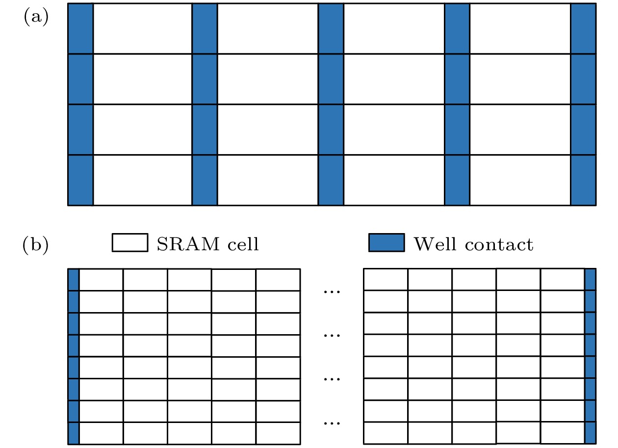
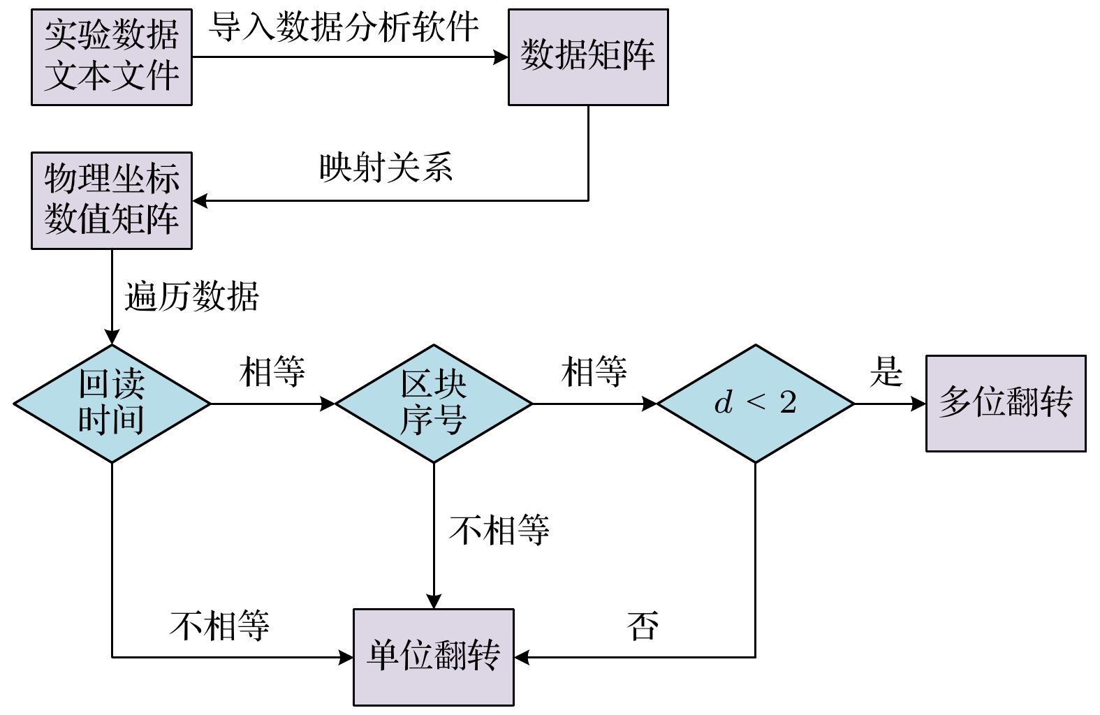
In order to study the effects of the feature size reduction and well contact placement on the characterization of topology patterns and the charge collection mechanism of device heavy ion single event multiple upset on a nanometer scale, the heavy ion single event effect experiment on the domestic 28 nm static random-access memory (SRAM) is carried out on the experimental platform of HI-13 heavy ion accelerator in Beijing. Based on the mapping relationship between the logical address and physical address of the device, the experimental data are processed, and the 28 nm SRAM heavy ion single event upset cross section curves, multiple upset percentage, and multiple upset topology patterns are obtained. The results are compared with those of heavy ion single event effect experiments in 65 nm SRAM, showing that under the influences of factors such as feature size reduction and lower operating voltage, the heavy ion single event upset threshold and the bit upset saturation cross section of 28 nm SRAM decrease significantly. In the direction perpendicular to the well, owing to the reduced 28 nm SRAM feature size, even if the single nucleon energy of the incident high LET (linear energy transfer) heavy ion is low, its deposited charge is sufficient to affect the three SRAM cells across the well direction due to the combined effect of ion track coverage, well potential modulation caused by the parasitic bipolar amplification effect and carrier diffusion, resulting in the fact that the 28 nm SRAM topology pattern has a shape of n rows × 3 columns, which poses new challenges and requirements for the anti-radiation hardened technology with scrubbing and EDAC (error detection and correction). Owing to the global well contact deployment, the charge deposited by the incident ions in the well far away from the well contact is difficult to discharge quickly, and the parasitic bipolar amplification effect lasts longer. The charge sharing competition between two p-channel metal oxide semiconductor in SRAM cell causes the single event upset recovery, which is the fundamental reason why the discontinuity of multiple upset topology pattern appears in 28 nm SRAM. This study provides a new anti-radiation hardened idea for suppressing the single event upset by using the parasitic bipolar amplification in the future.
-
Keywords:
- multiple cell upset /
- single event upset recovery /
- heavy ion /
- charge collection
[1] Narasimham B, Wang J K, Vedula N, Gupta S, Bartz B, Monzel C, Chatterjee I, Bharat B L, Schrimpf R D, Reed R A 2015 IEEE International Reliability Physics Symposium (IRPS) Mnterey, CA, USA, April 19–23, 2015 p2C.4.1
[2] Indranil C, Balaji N, Nihaar N M, Bharat L B, Ronald D S, Jung K W, Bartz B, Eswara P, Myron B 2011 IEEE Trans. Nucl. Sci. 58 2761
 Google Scholar
[3] Jeffrey D B, Paul E D, Kevin M W 2013 IEEE Trans. Nucl. Sci. 60 1836
 Google Scholar
[4] Anna B B, Armen V S, Anatoly A S, et al. 2015 IEEE Trans. Nucl. Sci. 62 2860
 Google Scholar
[5] Uros L, Anton B, Franc N 2012 IEEE Trans. Nucl. Sci. 59 2562
 Google Scholar
[6] Luo Y H, Zhang F Q, Chen W, Ding L L, Wang T 2021 IEEE Trans. Nucl. Sci. 68 1111
 Google Scholar
[7] Takashi K, Takashi Y, Kazunori M, Takashi S, Hiroaki I, Daisuke K, Kazuyuki H, Hideya M 2018 IEEE Trans. Nucl. Sci. 65 1900
 Google Scholar
[8] 王荣伟, 范国芳, 李博, 刘凡宇 2021 半导体技术 46 229
 Google Scholar
Wang R W, Fan G F, Li B, Liu F Y 2021 Semicond. Technol. 46 229
 Google Scholar
[9] 张战刚, 雷志峰, 童腾, 李晓辉, 王松林, 梁天骄, 习凯, 彭超, 何玉娟, 黄云, 恩云飞 2020 物理学报 69 056101
 Google Scholar
Zhang Z G, Lei Z F, Tong T, Li X H, Wang S L, Liang T J, Xi, Peng C, He Y J, Huang Y, En Y F 2020 Acta Phys. Sin. 69 056101
 Google Scholar
[10] Viyas G, Alexander B, Georgios T, Ali Z, Arto J, Ari V, Helmut P, Frederic S, Frederic W, Luigi D 2016 IEEE Trans. Nucl. Sci. 63 2010
 Google Scholar
[11] Maria K, Pablo F M, Ruben G A, Carlo C, Matteo C, Andrea C, Giuseppe L, Maris T, Nourdine K, Vanessa W, Johannes B, Salvatore D, Veronique F G, Alexander G, Henry W 2020 IEEE Trans. Nucl. Sci. 67 63
 Google Scholar
[12] Sun Y, Zhang H W, Wei Z C, Yu Q K, Tang M, Shen C, Gong D 2019 3rd International Conference on Circuits, System and Simulation (ICCSS) Nanjing, China, June 13–15, 2019 p84
[13] Farjallah E, Gherman V, Armani J M, Dilillo L 2018 3th International Conference on Design & Technology of Integrated Systems In Nanoscale Era (DTIS) Taormina, Italy, April 10–12, 2018 p1
[14] Wang J L, Jeffrey P, Andrea C, Sam T, Ruben G A, Paul L 2021 IEEE Trans. Nucl. Sci. 68 913
 Google Scholar
[15] Aditya K, Saini R, Kumar M, Singh R, Dixit A 2018 4th IEEE International Conference on Emerging Electronics (ICEE) Bengaluru, December 17–19, 2018 p1
[16] Slawosz U, Gilles G, Philippe R, Clement T, Jean L A 2010 IEEE Trans. Nucl. Sci. 57 1876
 Google Scholar
[17] 陶元, 甯德雄 著 (黄如, 王润声, 黎明, 蔡一茂, 谢倩, 安霞 译) 2020 现代VLSI器件基础(第二版) (北京: 电子工业出版社) 第45, 46页
Yuan T, Tak H N (translated by Huang R, Wang R S, Li M, Cai Y M, Xie Q, An X) 2020 Fundamentals of Modern VLSI Devices (2nd Ed.) (Beijing: Publishing House of Electronics Industry) pp45, 46 (in Chinese)
[18] Reed K, Andrew T K 2008 IEEE Trans. Nucl. Sci. 55 3367
 Google Scholar
[19] 赵雯 2020 博士学位论文 (西安: 西安交通大学)
Zhao W 2020 Ph. D. Dissertation (Xi’an: Xi’an Jiaotong University) (in Chinese)
[20] 李鹏, 张民选, 赵振宇, 邓全 2015 核技术(英文版) 26 050405
 Google Scholar
Li P, Zhang M X, Zhao Z Y, Deng Q 2015 Nucl. Sci. Technol. 26 050405
 Google Scholar
[21] Yang G Q, Yu J C, Liu X Y, Chen Q 2020 Electronics 9 927
 Google Scholar
[22] 金鑫, 唐民, 于庆奎, 张洪伟, 梅博, 孙毅, 唐路平 2019 电子与封装 19 32
 Google Scholar
Jin X, Tang M, Yu Q K, Zhang H W, Mei B, Sun Y, Tang L P 2019 Electron. Packag. 19 32
 Google Scholar
[23] 李鹏 2016 博士学位论文 (长沙: 国防科学技术大学)
Li P 2016 Ph. D. Dissertation (Changsha: National University of Defense Technology) (in Chinese)
[24] 赵雯, 郭晓强, 陈伟, 罗尹虹, 王汉宁 2018 电子学报 46 2495
 Google Scholar
Zhao W, Guo X Q, Chen W, Luo Y H, Wang H N 2018 Acta Electron. Sin. 46 2495
 Google Scholar
-
表 1 两款SRAM器件关键参数对比
Table 1. Key parameters of the 28 nm SRAM and 65 nm SRAM for comparison.
器件
名称SRAM单元
尺寸/μm2工作
电压/V容量 阱接触布放 65 nm
SRAM1.22×0.526 1.2 256 kbit 独立阱接触 28 nm
SRAM0.58×0.27 0.9 128 kbit 全局阱接触 表 2 实验所用的离子种类及其参数
Table 2. Ion species and parameters used in the experiment.
离子 能量/MeV 表面LET值
/(MeV·cm2·mg–1)硅中
射程/μmC 78 1.8 122 F 100 4.4 72.7 Si 135 9.3 50.7 I 283 65.6 30.0 -
[1] Narasimham B, Wang J K, Vedula N, Gupta S, Bartz B, Monzel C, Chatterjee I, Bharat B L, Schrimpf R D, Reed R A 2015 IEEE International Reliability Physics Symposium (IRPS) Mnterey, CA, USA, April 19–23, 2015 p2C.4.1
[2] Indranil C, Balaji N, Nihaar N M, Bharat L B, Ronald D S, Jung K W, Bartz B, Eswara P, Myron B 2011 IEEE Trans. Nucl. Sci. 58 2761
 Google Scholar
[3] Jeffrey D B, Paul E D, Kevin M W 2013 IEEE Trans. Nucl. Sci. 60 1836
 Google Scholar
[4] Anna B B, Armen V S, Anatoly A S, et al. 2015 IEEE Trans. Nucl. Sci. 62 2860
 Google Scholar
[5] Uros L, Anton B, Franc N 2012 IEEE Trans. Nucl. Sci. 59 2562
 Google Scholar
[6] Luo Y H, Zhang F Q, Chen W, Ding L L, Wang T 2021 IEEE Trans. Nucl. Sci. 68 1111
 Google Scholar
[7] Takashi K, Takashi Y, Kazunori M, Takashi S, Hiroaki I, Daisuke K, Kazuyuki H, Hideya M 2018 IEEE Trans. Nucl. Sci. 65 1900
 Google Scholar
[8] 王荣伟, 范国芳, 李博, 刘凡宇 2021 半导体技术 46 229
 Google Scholar
Wang R W, Fan G F, Li B, Liu F Y 2021 Semicond. Technol. 46 229
 Google Scholar
[9] 张战刚, 雷志峰, 童腾, 李晓辉, 王松林, 梁天骄, 习凯, 彭超, 何玉娟, 黄云, 恩云飞 2020 物理学报 69 056101
 Google Scholar
Zhang Z G, Lei Z F, Tong T, Li X H, Wang S L, Liang T J, Xi, Peng C, He Y J, Huang Y, En Y F 2020 Acta Phys. Sin. 69 056101
 Google Scholar
[10] Viyas G, Alexander B, Georgios T, Ali Z, Arto J, Ari V, Helmut P, Frederic S, Frederic W, Luigi D 2016 IEEE Trans. Nucl. Sci. 63 2010
 Google Scholar
[11] Maria K, Pablo F M, Ruben G A, Carlo C, Matteo C, Andrea C, Giuseppe L, Maris T, Nourdine K, Vanessa W, Johannes B, Salvatore D, Veronique F G, Alexander G, Henry W 2020 IEEE Trans. Nucl. Sci. 67 63
 Google Scholar
[12] Sun Y, Zhang H W, Wei Z C, Yu Q K, Tang M, Shen C, Gong D 2019 3rd International Conference on Circuits, System and Simulation (ICCSS) Nanjing, China, June 13–15, 2019 p84
[13] Farjallah E, Gherman V, Armani J M, Dilillo L 2018 3th International Conference on Design & Technology of Integrated Systems In Nanoscale Era (DTIS) Taormina, Italy, April 10–12, 2018 p1
[14] Wang J L, Jeffrey P, Andrea C, Sam T, Ruben G A, Paul L 2021 IEEE Trans. Nucl. Sci. 68 913
 Google Scholar
[15] Aditya K, Saini R, Kumar M, Singh R, Dixit A 2018 4th IEEE International Conference on Emerging Electronics (ICEE) Bengaluru, December 17–19, 2018 p1
[16] Slawosz U, Gilles G, Philippe R, Clement T, Jean L A 2010 IEEE Trans. Nucl. Sci. 57 1876
 Google Scholar
[17] 陶元, 甯德雄 著 (黄如, 王润声, 黎明, 蔡一茂, 谢倩, 安霞 译) 2020 现代VLSI器件基础(第二版) (北京: 电子工业出版社) 第45, 46页
Yuan T, Tak H N (translated by Huang R, Wang R S, Li M, Cai Y M, Xie Q, An X) 2020 Fundamentals of Modern VLSI Devices (2nd Ed.) (Beijing: Publishing House of Electronics Industry) pp45, 46 (in Chinese)
[18] Reed K, Andrew T K 2008 IEEE Trans. Nucl. Sci. 55 3367
 Google Scholar
[19] 赵雯 2020 博士学位论文 (西安: 西安交通大学)
Zhao W 2020 Ph. D. Dissertation (Xi’an: Xi’an Jiaotong University) (in Chinese)
[20] 李鹏, 张民选, 赵振宇, 邓全 2015 核技术(英文版) 26 050405
 Google Scholar
Li P, Zhang M X, Zhao Z Y, Deng Q 2015 Nucl. Sci. Technol. 26 050405
 Google Scholar
[21] Yang G Q, Yu J C, Liu X Y, Chen Q 2020 Electronics 9 927
 Google Scholar
[22] 金鑫, 唐民, 于庆奎, 张洪伟, 梅博, 孙毅, 唐路平 2019 电子与封装 19 32
 Google Scholar
Jin X, Tang M, Yu Q K, Zhang H W, Mei B, Sun Y, Tang L P 2019 Electron. Packag. 19 32
 Google Scholar
[23] 李鹏 2016 博士学位论文 (长沙: 国防科学技术大学)
Li P 2016 Ph. D. Dissertation (Changsha: National University of Defense Technology) (in Chinese)
[24] 赵雯, 郭晓强, 陈伟, 罗尹虹, 王汉宁 2018 电子学报 46 2495
 Google Scholar
Zhao W, Guo X Q, Chen W, Luo Y H, Wang H N 2018 Acta Electron. Sin. 46 2495
 Google Scholar
Catalog
Metrics
- Abstract views: 7118
- PDF Downloads: 95
- Cited By: 0


 DownLoad:


