


-
Energy funneling effect of two-dimensional materials provides an important method for modulating carrier transfer. However, the formation of energy funneling and its influences on the carrier transfer are still relatively uncharacterized. In this work, the energy funneling induced by the layer number gradient effect in MoS2 is investigated through atomic-bond-relaxation approach and first-principles calculations. It is found that the bandgap of MoS2 monotonically increases with the decrease of the layer number, leading the conduction band minimum (valence band maximum) of thin layer MoS2 to be higher than (lower than) that of thick layer MoS2. Therefore, both dual thickness gradient and triple thickness gradient MoS2 can achieve the energy funneling effect. As a result, the carriers will be directionally transferred from the thin layer region to the thick layer region. According to Marcus theory, the carrier transfer rate is dependent on drive force caused by the energy level difference with different thicknesses of MoS2. For the dual thickness gradient MoS2, when the thickness difference between adjacent layers is the largest, the driving force is the highest, which is 1L/bulk. In addition, owing to the driving force smaller than the reorganization energy in dual thickness gradient MoS2, a large driving force corresponds to a high carrier transfer rate, resulting in a higher carrier transfer rate of 1L/bulk than those in other dual thickness gradient systems. For the triple thickness gradient MoS2, there are two consecutive interface energy differences that induce driving forces. However, the carrier transfer rate is exponentially correlated with the driving force. Therefore, the carrier transfer rate of dual thickness gradient MoS2 will be higher than that of the corresponding triple thickness gradient MoS2. Our results demonstrate that the energy funneling effect induced by thickness gradient can realize carrier accumulation in the thick layer region without the need for p-n junctions, which is of great benefit in collecting photogenerated carriers. The atomic force microscopy lithography and chemical vapor deposition will be used to engineer thickness-gradient two-dimensional materials with enhanced optoelectronic properties in future.
-
Keywords:
- MoS2 /
- thickness gradient /
- energy funneling effect
[1] Jiang H, Zhang X K, Chen K L, He X Y, Liu Y H, Yu H H, Gao L, Hong M Y, Wang Y, Zhang Z, Zhang Y 2025 Nat. Mater. 24 188
 Google Scholar
[2] Zhao J J, Liao M Z, Shen C, Wang Q Q, Yang R, Watanabe K, Taniguchi T, Huang Z H, Shi D X, Liu K H, Sun Z P, Feng J, Du L J, Zhang G Y 2025 Phys. Rev. Lett. 134 086201
Google Scholar
[3] Mak K F, Lee C, Hone J, Shan J, Heinz T F 2010 Phys. Rev. Lett. 105 136805
Google Scholar
[4] Li L K, Yu Y J, Ye G J, Ge Q Q, Ou X D, Wu H, Feng D L, Chen X H, Zhang Y B 2014 Nat. Nanotechnol. 9 372
Google Scholar
[5] 邓文, 汪礼胜, 刘嘉宁, 余雪玲, 陈凤翔 2021 物理学报 70 217302
Google Scholar
Deng W, Wang L S, Liu J N, Yu X L, Chen F X 2021 Acta Phys. Sin. 70 217302
Google Scholar
[6] Yang F, Hu Y T, Ou J L, Li Q Y, Xie X X, Han H P, Cai C L, Ruan S C, Xiang B X 2025 ACS Photonics 12 2128
Google Scholar
[7] Feng J, Qian X F, Huang C W, Li J 2012 Nat. Photonics 6 866
Google Scholar
[8] Li H, Contryman A W, Qian X F, Ardakani S M, Gong Y J, Wang X L, Weisse J M, Lee C H, Zhao J H, Ajayan P M, Li J, Manoharan H C, Zheng X L 2015 Nat. Commun. 6 7381
Google Scholar
[9] Harats M G, Kirchhof J N, Qiao M X, Greben K, Bolotin K I 2020 Nat. Photonics 14 324
Google Scholar
[10] Lee J, Yun S J, Seo C, Cho K, Kim T S, An G H, Kang K, Lee H S, Kim J 2021 Nano Lett. 21 43
Google Scholar
[11] 刘俊杰, 左慧玲, 谭鑫, 董健生 2024 物理学报 73 236801
Google Scholar
Liu J J, Zuo H L, Tan X, Dong J S 2024 Acta Phys. Sin. 73 236801
Google Scholar
[12] Sun Z Y, Li Y, Xu B, Chen H, Wang P, Zhao S X, Li Y, Gao B, Dou X M, Sun B Q, Zhen L, Xu C Y 2021 Adv. Opt. Mater. 9 2100438
Google Scholar
[13] Xu N, Pei X D, Qiu L P, Zhan L, Wang P, Shi Y, Li S L 2023 Adv. Mater. 35 2300618
Google Scholar
[14] Ouyang G, Wang C X, Yang G W 2009 Chem. Rev. 109 4221
Google Scholar
[15] Zhu Z M, Zhang A, Ouyang G, Yang G W 2011 Appl. Phys. Lett. 98 263112
Google Scholar
[16] Dong J S, Zhao Y P, Ouyang G, Yang G W 2022 Appl. Phys. Lett. 120 080501
Google Scholar
[17] Sun C Q 2007 Prog. Solid State Chem. 35 1
Google Scholar
[18] Jiang J W, Park H S, Rabczuk T 2013 J. Appl. Phys. 114 064307
Google Scholar
[19] Xiong S, Cao G X 2015 Nanotechnology 26 185705
Google Scholar
[20] Zhu Y F, Jiang Q 2016 Coordin. Chem. Rev. 326 1
Google Scholar
[21] Marcus R A 1956 J. Chem. Phys. 24 966
Google Scholar
[22] Zhang C, Lian L Y, Yang Z L, Zhang J B, Zhu H M 2019 J. Phys. Chem. Lett. 10 7665
Google Scholar
[23] Kresse G, Hafner J. 1993 Phys. Rev. B 47 558
Google Scholar
[24] Blöchl P E 1994 Phys. Rev. B 50 17953
Google Scholar
[25] Kresse G 1996 Phys. Rev. B 54 11169
Google Scholar
[26] Yun W S, Han S W, Hong S C, Kim I G, Lee J D 2012 Phys. Rev. B 85 033305
Google Scholar
[27] Li T S 2012 Phys. Rev. B 85 235407
Google Scholar
[28] Kang J, Tongay S, Zhou J, Li J B, Wu J Q 2013 Appl. Phys. Lett. 102 012111
Google Scholar
[29] Dong J S, Liu J J, Liao W H, Yang X X, He Y, Ouyang G 2024 J. Appl. Phys. 136 125302
Google Scholar
[30] Chu T, Ilatikhameneh H, Klimeck G, Rahman R, Chen Z H 2015 Nano Lett. 15 8000
Google Scholar
[31] Lee H S, Min S W, Chang Y G, Park M K, Nam T, Kim H, Kim J H, Ryu S, Im S 2012 Nano Lett. 12 3695
Google Scholar
[32] Wang J H, Ding T, Gao K M, Wang L F, Zhou P W, Wu K F 2021 Nat. Commun. 12 6333
Google Scholar
[33] Furchi M M, Pospischil A, Libisch F, Burgdörfer J, Mueller T 2014 Nano Lett. 14 4785
Google Scholar
[34] Lee C H, Lee G H, Zande A M, Chen W C, Li Y L, Han M Y, Cui X, Arefe G, Nuckolls C, Heinz T F, Guo J, Hone J, Kim P 2014 Nat. Nanotechnol. 9 676
Google Scholar
[35] Cao G Y, Shang A X, Zhang C, Gong Y P, Li S J, Bao Q L, Li X F 2016 Nano Energy 30 260
Google Scholar
-
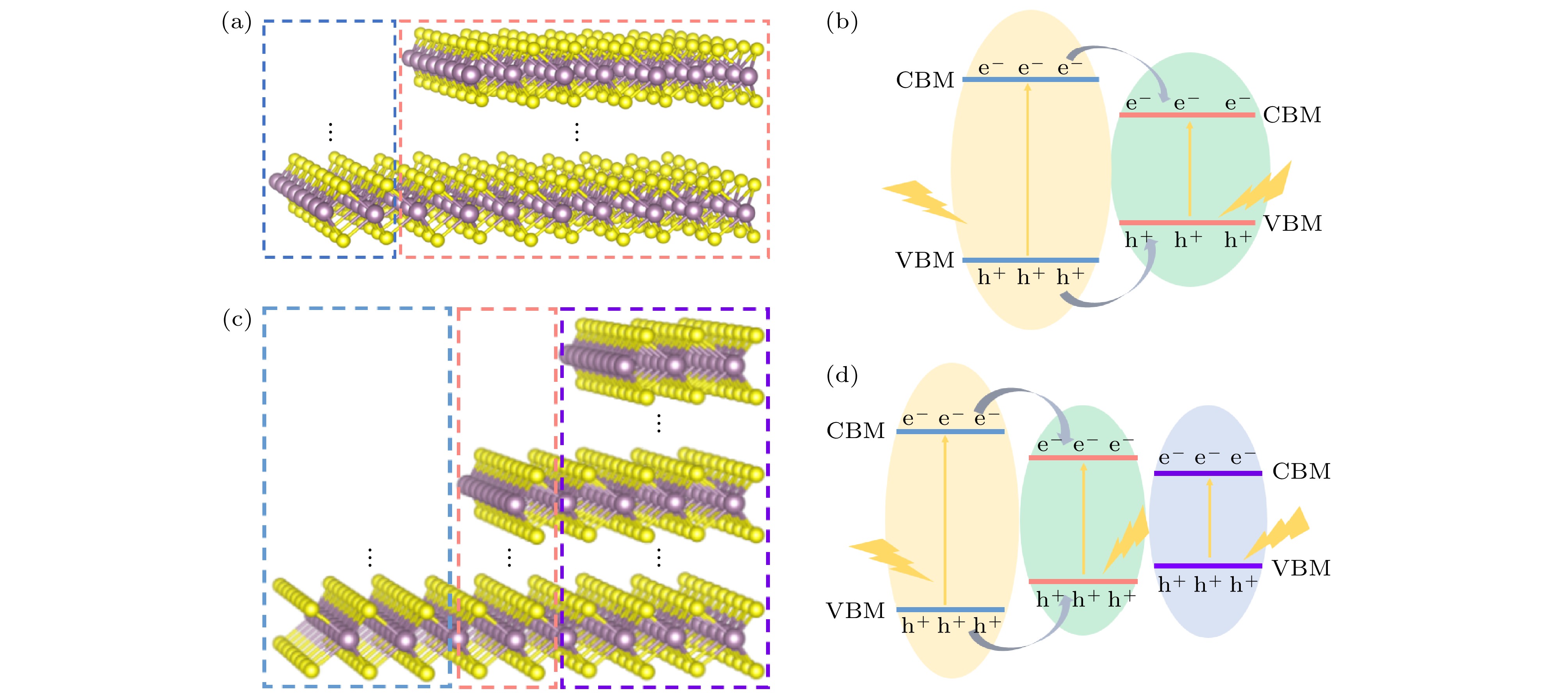
图 1 (a) 双厚度梯度MoS2结构示意图; (b) 双厚度梯度MoS2能带漏斗及其对电荷转移示意图; (c) 三厚度梯度MoS2结构示意图; (d) 三厚度梯度MoS2能带漏斗及其对电荷转移示意图
Figure 1. (a) Schematic diagrams of dual thickness gradient MoS2; (b) energy funneling and its effect on carrier transfer in dual thickness gradient MoS2; (c) schematic diagrams of triple thickness gradient MoS2; (d) energy funneling and its effect on carrier transfer in triple thickness gradient MoS2.
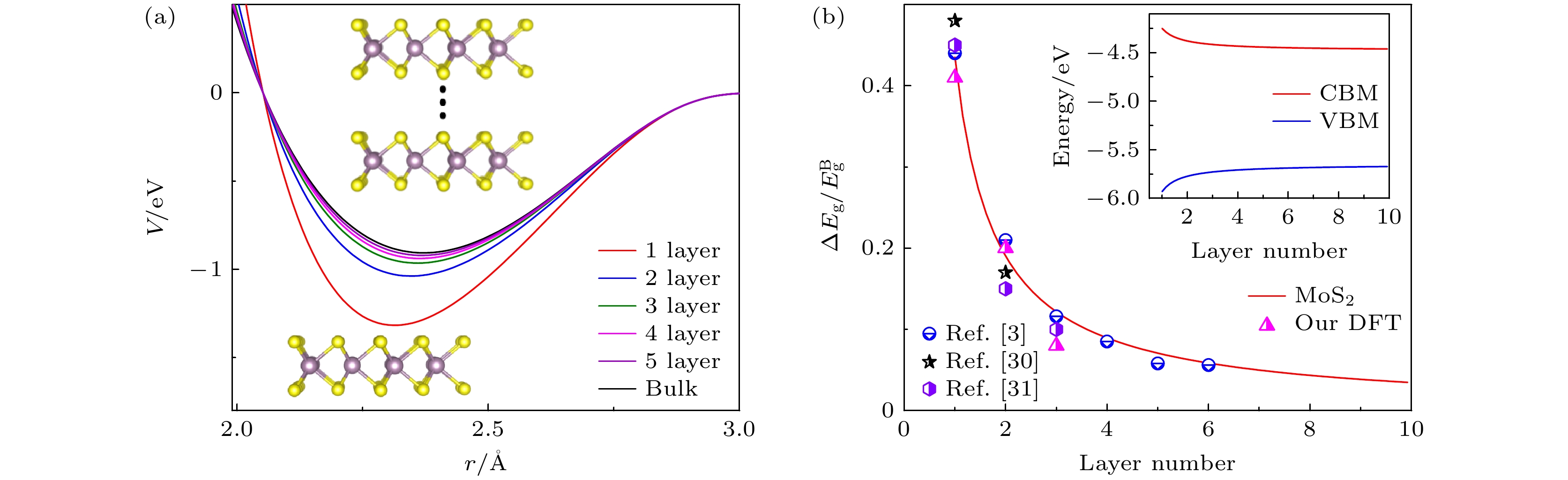
图 2 (a) 不同层数MoS2势函数与原子间距之间的关系; (b) MoS2层数依赖的带隙漂移, 插图是MoS2导带底和价带顶随层数的变化规律
Figure 2. (a) Relationship between potential and distance of MoS2 with different layer number; (b) layer number dependent bandgap of MoS2, the inset of (b) shows the conduction band minimum (CBM) and valence band maximum (VBM) of MoS2 as a function of layer number.
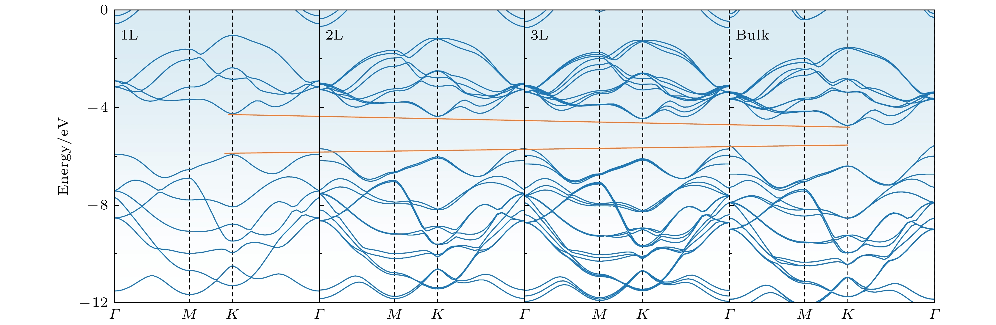
图 3 不同层数MoS2的能带结构
Figure 3. Band structures of MoS2 with different layer.
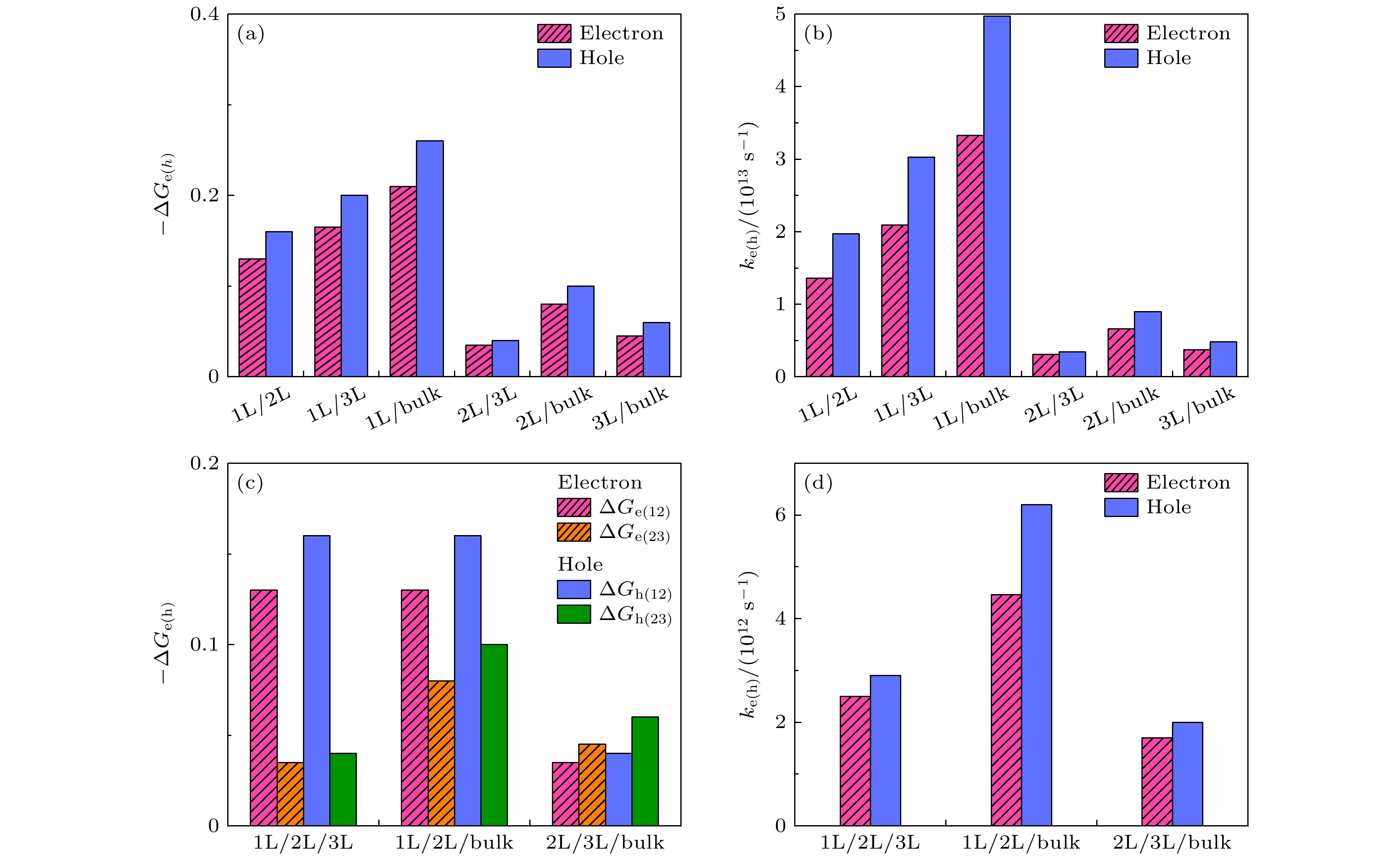
图 4 (a) 双厚度梯度MoS2界面能级差诱导的驱动力; (b) 双厚度梯度MoS2中的能带漏斗对电荷转移速率影响; (c) 三厚度梯度MoS2界面能级差诱导的驱动力; (d) 三厚度梯度MoS2中的能带漏斗对电荷转移速率影响
Figure 4. (a) Driving force induced by the energy level difference in dual thickness gradient MoS2; (b) the effect of energy funneling on the charge transfer rate in dual thickness gradient MoS2; (c) the driving force induced by the energy level difference in triple thickness gradient MoS2; (d) the effect of energy funneling on the charge transfer rate in triple thickness gradient MoS2.
-
[1] Jiang H, Zhang X K, Chen K L, He X Y, Liu Y H, Yu H H, Gao L, Hong M Y, Wang Y, Zhang Z, Zhang Y 2025 Nat. Mater. 24 188
Google Scholar
[2] Zhao J J, Liao M Z, Shen C, Wang Q Q, Yang R, Watanabe K, Taniguchi T, Huang Z H, Shi D X, Liu K H, Sun Z P, Feng J, Du L J, Zhang G Y 2025 Phys. Rev. Lett. 134 086201
Google Scholar
[3] Mak K F, Lee C, Hone J, Shan J, Heinz T F 2010 Phys. Rev. Lett. 105 136805
Google Scholar
[4] Li L K, Yu Y J, Ye G J, Ge Q Q, Ou X D, Wu H, Feng D L, Chen X H, Zhang Y B 2014 Nat. Nanotechnol. 9 372
Google Scholar
[5] 邓文, 汪礼胜, 刘嘉宁, 余雪玲, 陈凤翔 2021 物理学报 70 217302
Google Scholar
Deng W, Wang L S, Liu J N, Yu X L, Chen F X 2021 Acta Phys. Sin. 70 217302
Google Scholar
[6] Yang F, Hu Y T, Ou J L, Li Q Y, Xie X X, Han H P, Cai C L, Ruan S C, Xiang B X 2025 ACS Photonics 12 2128
Google Scholar
[7] Feng J, Qian X F, Huang C W, Li J 2012 Nat. Photonics 6 866
Google Scholar
[8] Li H, Contryman A W, Qian X F, Ardakani S M, Gong Y J, Wang X L, Weisse J M, Lee C H, Zhao J H, Ajayan P M, Li J, Manoharan H C, Zheng X L 2015 Nat. Commun. 6 7381
Google Scholar
[9] Harats M G, Kirchhof J N, Qiao M X, Greben K, Bolotin K I 2020 Nat. Photonics 14 324
Google Scholar
[10] Lee J, Yun S J, Seo C, Cho K, Kim T S, An G H, Kang K, Lee H S, Kim J 2021 Nano Lett. 21 43
Google Scholar
[11] 刘俊杰, 左慧玲, 谭鑫, 董健生 2024 物理学报 73 236801
Google Scholar
Liu J J, Zuo H L, Tan X, Dong J S 2024 Acta Phys. Sin. 73 236801
Google Scholar
[12] Sun Z Y, Li Y, Xu B, Chen H, Wang P, Zhao S X, Li Y, Gao B, Dou X M, Sun B Q, Zhen L, Xu C Y 2021 Adv. Opt. Mater. 9 2100438
Google Scholar
[13] Xu N, Pei X D, Qiu L P, Zhan L, Wang P, Shi Y, Li S L 2023 Adv. Mater. 35 2300618
Google Scholar
[14] Ouyang G, Wang C X, Yang G W 2009 Chem. Rev. 109 4221
Google Scholar
[15] Zhu Z M, Zhang A, Ouyang G, Yang G W 2011 Appl. Phys. Lett. 98 263112
Google Scholar
[16] Dong J S, Zhao Y P, Ouyang G, Yang G W 2022 Appl. Phys. Lett. 120 080501
Google Scholar
[17] Sun C Q 2007 Prog. Solid State Chem. 35 1
Google Scholar
[18] Jiang J W, Park H S, Rabczuk T 2013 J. Appl. Phys. 114 064307
Google Scholar
[19] Xiong S, Cao G X 2015 Nanotechnology 26 185705
Google Scholar
[20] Zhu Y F, Jiang Q 2016 Coordin. Chem. Rev. 326 1
Google Scholar
[21] Marcus R A 1956 J. Chem. Phys. 24 966
Google Scholar
[22] Zhang C, Lian L Y, Yang Z L, Zhang J B, Zhu H M 2019 J. Phys. Chem. Lett. 10 7665
Google Scholar
[23] Kresse G, Hafner J. 1993 Phys. Rev. B 47 558
Google Scholar
[24] Blöchl P E 1994 Phys. Rev. B 50 17953
Google Scholar
[25] Kresse G 1996 Phys. Rev. B 54 11169
Google Scholar
[26] Yun W S, Han S W, Hong S C, Kim I G, Lee J D 2012 Phys. Rev. B 85 033305
Google Scholar
[27] Li T S 2012 Phys. Rev. B 85 235407
Google Scholar
[28] Kang J, Tongay S, Zhou J, Li J B, Wu J Q 2013 Appl. Phys. Lett. 102 012111
Google Scholar
[29] Dong J S, Liu J J, Liao W H, Yang X X, He Y, Ouyang G 2024 J. Appl. Phys. 136 125302
Google Scholar
[30] Chu T, Ilatikhameneh H, Klimeck G, Rahman R, Chen Z H 2015 Nano Lett. 15 8000
Google Scholar
[31] Lee H S, Min S W, Chang Y G, Park M K, Nam T, Kim H, Kim J H, Ryu S, Im S 2012 Nano Lett. 12 3695
Google Scholar
[32] Wang J H, Ding T, Gao K M, Wang L F, Zhou P W, Wu K F 2021 Nat. Commun. 12 6333
Google Scholar
[33] Furchi M M, Pospischil A, Libisch F, Burgdörfer J, Mueller T 2014 Nano Lett. 14 4785
Google Scholar
[34] Lee C H, Lee G H, Zande A M, Chen W C, Li Y L, Han M Y, Cui X, Arefe G, Nuckolls C, Heinz T F, Guo J, Hone J, Kim P 2014 Nat. Nanotechnol. 9 676
Google Scholar
[35] Cao G Y, Shang A X, Zhang C, Gong Y P, Li S J, Bao Q L, Li X F 2016 Nano Energy 30 260
Google Scholar

 DownLoad:
Catalog
Metrics
- Abstract views: 1329
- PDF Downloads: 26
- Cited By: 0
